
Battery Monitoring System PCB: Why the Hardware Foundation Determines Everything Else
BMS reliability isn’t decided by algorithms — it’s decided by the PCB
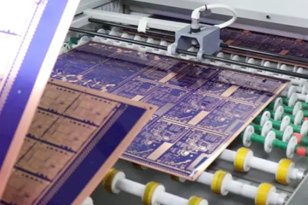
I recently discovered an interesting phenomenon while researching circuit board design in network equipment. Many people, when they think of HDI PCB networks, think of ultra-thin optical module boards or densely packed switch motherboards, but I believe that what truly tests technical prowess is actually those inconspicuous backplanes.
I remember once visiting a factory and seeing a large backplane with more than 50 layers running on a test fixture. The engineer pointed to the densely packed vias and said, “The real challenge lies in signal transmission on such thick boards. Focusing solely on thinness can neglect the stability of the underlying structure.”
There’s a misconception in the industry right now: everyone talks about millimeter-level precision. But in practical applications, ordinary multilayer boards with errors controlled within 0.05mm are often more reliable than designs that prioritize extreme thinness. Like building a house, a solid foundation is more important than the tiles on the exterior walls.
I’ve seen too many cases where heat dissipation was sacrificed to make the board thinner than 0.8mm. Especially in high-temperature environments, slightly thicker boards maintain more stable electrical characteristics. This reminds me of the military communication equipment I worked with years ago; their circuit boards were never designed for thinness.
Actually, judging the quality of a board is simple—run it continuously for two weeks. Those that can withstand prolonged high loads are truly proven designs. After all, the biggest fear for network equipment isn’t size, but failure at critical moments.
Sometimes, looking at those prototype boards in the lab pushing the limits of specifications, I find myself appreciating the seemingly ordinary yet durable conventional designs on mass production lines. After all, in practical applications, stability and reliability are paramount.
I recently chatted with some friends who work on network equipment and noticed an interesting phenomenon. These days, when people talk about HDI PCBs, they tend to obsess over ultra-high density, as if more layers equate to superior performance. This view is quite one-sided. Those in the know understand that good design should prioritize performance while simplifying.
I’ve seen many engineers design boards like a mille-feuille to achieve impressive specifications. The result? Unresolved heat dissipation issues and a plummeting yield rate. I remember a project that used an 8-layer HDI board, ultimately having to revert to a 6-layer design due to inadequate heat dissipation. Sometimes, less is more, a principle particularly applicable in PCB design.
Regarding material selection, there’s a worrying trend in the industry: blindly pursuing the latest models. Some insist on using M9-grade substrates for ordinary network devices, which is like putting a sports car engine in a family car—a pure waste of resources. In reality, for most network devices, compatibility is key. I learned this the hard way in a base station project I handled; using materials beyond what was required caused costs to skyrocket by 30%, with negligible performance improvements.
Many manufacturers like to hype the CPO (Consumer-on-Profile) concept, but frankly, there aren’t many truly viable examples at this stage. Instead of blindly following trends, it’s better to solidify the foundation first. For example, in our data center switch project last year, we improved signal integrity by 20% by optimizing cabling design—far more effective than simply adopting new technologies.
Embedded components are indeed a good direction, but it depends on the specific application scenario. I once saw a router design that embedded all passive components, resulting in extremely difficult debugging later. My experience is that components on critical signal paths are more prudently placed on the surface.
When choosing a supplier, I think you can’t just look at technical specifications. A previous HDI PCB network supplier, while not having the most cutting-edge equipment, had a very reliable engineering team that frequently offered constructive suggestions. This kind of soft power is often more important than hard specifications.
Ultimately, PCB design is an art of balance. Being too aggressive can lead to pitfalls, while being too conservative will leave you behind. The ideal approach is to keep up with technological trends while maintaining a clear head. After all, we’re developing products, not lab prototypes.
Recently, while chatting with a friend who works in the telecommunications equipment industry, I mentioned that their company is upgrading its production line to use Ultra-level HDI boards. It suddenly dawned on me that the iteration speed of network equipment is so fast that even basic hardware is being redefined. Previously, I always thought of PCBs as simply boards that carry components, but high-density interconnect technology has elevated the entire system’s performance to a new level.
I’ve seen traditional PCB designs in network equipment where the traces meander like a maze, resulting in significant signal latency issues. The real power of HDI technology lies in its ability to make circuit layouts incredibly compact, like compressing an eight-lane highway into a three-dimensional transportation hub. This not only saves space but also reduces signal transmission loss. This change is revolutionary for network equipment that needs to process massive amounts of data in real time.
An interesting phenomenon is that many manufacturers now frantically increase the number of layers when they hear about HDI. However, blindly pursuing more layers actually increases costs. The key is to balance density and reliability. For example, some edge routers can achieve the functionality of a 10-layer board with only 6 layers of HDI. This is a shift in design thinking. We need to focus more on how to achieve optimal performance through reasonable layer stacking design. The shortest signal path, not simply increasing the number of microvias.
Last year, I visited a data center and saw that their core switches used HDI motherboards with arbitrary layer interconnects. The engineers said this design improved heat dissipation efficiency by over 30% because the components were more densely packed, making heat dissipation easier. This made me realize that the development of network equipment has long since moved beyond simply pursuing speed; stability and heat dissipation capabilities have become the focus of competition for high-end equipment.
Many people are now discussing the hardware requirements of 5G and AI, but I think what truly drives the evolution of HDI technology is the stringent reliability requirements of network equipment itself. For example, base station equipment needs to operate continuously for several years in extreme environments, which places higher demands on the durability of the circuit board. Ordinary PCBs may show signs of aging after two years, while high-quality HDI boards can significantly extend the equipment’s lifespan.
In fact, when choosing an HDI solution, it’s unnecessary to blindly pursue the highest specifications. In some scenarios, 2nd-order HDI is sufficient to handle most network transmission needs. The key is to make judgments based on actual bandwidth and power consumption. Just like decorating a house, not every room needs marble floors; composite flooring is more practical in some places.
I think many people have a misconception about HDI PCBs—they always think that more layers mean more advanced technology. In reality, what network equipment truly tests is stability and compatibility design. Last year, our team worked on a project using a 20-layer PCB from another manufacturer, which resulted in severe signal interference. Switching to a 12-layer HDI PCB network architecture resolved the issue.
Sometimes suppliers show you a bunch of certifications, but in actual production, they can’t even perform basic impedance testing properly. I’ve seen manufacturers with UL certification whose production lines lack proper temperature and humidity monitoring, leading to PCB warping due to moisture.
Truly reliable manufacturers will proactively discuss their testing processes, such as how they use X-rays to inspect microvia structures or high-frequency signal loss data, rather than just boasting about their high layer count.
I remember once during a factory audit, we noticed a detail: they reserved samples for each batch for dedicated aging tests. This hands-on approach is far more convincing than a wall full of certifications.
Many small factories are now jumping on the bandwagon with high-layer PCBs, but they can’t even control basic trace tolerances. Having learned our lesson, we now value manufacturers’ understanding of material properties, such as the stability of the dielectric layer at different frequencies.
The factory we recently partnered with isn’t large, but their engineers would bring an impedance meter to adjust parameters on-site. This pragmatic attitude is far more effective than those who just talk about 100-layer technology.
Ultimately, choosing an HDI PCB isn’t about selecting parameters, but about choosing a partner who is willing to invest the time to understand your application scenario.
I’ve always felt that many people’s understanding of HDI PCBs is too limited. They spend ages staring at parameter tables and technical specifications. But what truly interests me is how these circuit boards function in everyday network equipment.
I remember last year when I disassembled my home router, I found the motherboard was much more compact than I expected. The gaps between the traces might only be a few millimeters wide, yet it had to handle a massive amount of data flow. This precise layout made me realize how demanding modern network equipment is in terms of space utilization.
Once, I discussed this topic with a friend who does hardware design. He mentioned that many manufacturers are now focusing on more flexible routing solutions. Traditional design thinking always pursues layer stacking, but in practical applications, targeted optimization is often needed based on specific functional modules.
I’ve seen some failed cases where designers focused too much on theoretically perfect density, neglecting actual heat dissipation requirements. After operating in high-temperature environments for a few hours, the performance of the circuit board begins to fluctuate; this is particularly noticeable in network equipment that operates for extended periods.
Good HDI design, like urban planning, should ensure smooth traffic flow while providing sufficient buffer zones. Simply pursuing high density without considering signal interference is like driving fast in a narrow alley – it’s bound to cause problems sooner or later.
Recently, I’ve noticed some manufacturers starting to try layering different functional circuits, placing critical signals on inner layers and ordinary circuits on outer layers. This approach is more practical than simply stacking microvias; at least from a maintenance perspective, modular design makes troubleshooting easier.
Ultimately, technical parameters are just tools. The real challenge lies in ensuring these delicate circuits operate stably throughout the entire lifecycle of the network equipment. After all, nobody wants their network equipment to frequently disconnect due to overheating or signal crosstalk.
Whenever I talk to engineer friends about HDI board selection, someone always brings up technical parameters. I think those specifications are just an entry ticket. What truly determines the success or failure of a project is often what’s hidden behind the specifications.
Last year, we had a base station project where the supplier’s technical documentation was incredibly detailed, but during the sample stage, we discovered absurdly poor impedance consistency. Later, I switched to a well-established manufacturer specializing in communications. Although the price was 15% higher, their engineers brought their solutions and were on-site for debugging. This understanding of application scenarios goes far beyond what specifications can convey.
Many buyers are now attracted by the global reach of HDI manufacturers, but anyone who has experienced supply chain fluctuations knows that global capacity is a double-edged sword. Once, when urgently needing to order more stock, a large manufacturer was delayed by two weeks due to cross-border coordination, while a local mid-sized supplier saved the day with flexible production line adjustments. Response speed in critical moments is often more valuable than factory layout diagrams.
I particularly value how suppliers accumulate technical expertise. Manufacturers like TTM actively participate in the early design phase, and their engineering suggestions often prevent extensive modifications later. Once, when working on high-speed backplane connections, their proposed stacked solution eliminated six laser holes, improving reliability and reducing costs by 10%. This value goes beyond ordinary sales transactions.
Recently, while evaluating HDI boards for 5G small cells, I discovered that some emerging manufacturers are very willing to invest in material innovation. Their low-loss dielectric material, while having a higher initial cost, can reduce base station power consumption by about 8%. This long-term technological investment is far more meaningful than simply comparing prices.
Choosing an HDI supplier is like finding a partner; focusing solely on hardware configurations can easily lead to problems. What truly matters is whether the supplier is willing to deeply understand your product logic and can translate their technological expertise into practical solutions. After all, even the most advanced PCB technology must ultimately be effective in specific devices.
Recently, conversations with several friends in hardware procurement revealed that when selecting HDI PCB network equipment, people tend to get bogged down in comparing technical parameters, neglecting the most fundamental issues. After handling several data center upgrade projects, I’ve found that what truly influences decisions is often not those on-paper specifications.
I remember a project last year where the supplier’s HDI sample outperformed competitors in every aspect, but a flaw in the thermal design was only discovered during actual deployment in the core switch. This kind of problem is impossible to detect during the testing phase; it only surfaced after three months of full-load operation. Therefore, I now pay more attention to the manufacturer’s actual application cases when evaluating PCB products.
Many people believe that choosing a high-density interconnect (HDI) board is simply about who has the finest line width and spacing. However, the lamination process and material stability are actually key. During a factory visit, I discovered that some manufacturers cut corners in the fiberglass cloth pretreatment stage, leading to delamination later on, even with the same specifications. These details are often more important than the technical specifications.
With network equipment evolving so rapidly, compatibility for the next three to five years must be considered during procurement. For example, while the special interface designs used in certain AI computing clusters may be cutting-edge now, they can become a burden if industry standards change. I prefer suppliers with solid fundamental processes and the ability to flexibly adjust solutions.
Sometimes, niche manufacturers can offer more practical solutions. One German manufacturer’s HDI products, while not boasting outstanding specifications, have unique advantages in impedance control, with measured performance exceeding that of major manufacturers at a price 20% lower. This requires the purchasing party to invest time in researching.
Ultimately, selection shouldn’t rely solely on technical documents; it’s essential to visit factories and observe real-world application scenarios. During my last visit to Shenzhen to inspect production lines, I discovered that some manufacturers of PCBs, even those supposedly rated as 8 layers, were doing a very perfunctory job with blind and buried vias. This directly impacts the long-term stability of network equipment.
I think there’s a misconception in the industry right now: an excessive pursuit of cutting-edge technology at the expense of fundamental reliability. This is especially true for HDI boards used in core network equipment. It’s better to be conservative with specifications to ensure absolute reliability. After all, the losses from network outages far outweigh hardware costs.
Regarding the selection of HDI PCB network equipment, I have a slightly different perspective. Many people immediately pursue the highest specifications, but in most scenarios, such extreme technical parameters are unnecessary. Last year, our team conducted a comparative test and found that the performance difference between ordinary 4-layer boards and high-end HDI boards in certain industrial scenarios was less than 5%, but the cost difference was nearly three times.
Many manufacturers now like to package HDI technology as a panacea. Once, I visited a factory and saw that their production line was still using old equipment, yet they were able to achieve the signal integrity requirements of new equipment by optimizing the wiring design. This made me realize that when choosing a supplier, you can’t just look at the technical specifications; you need to actually assess whether their engineering team has the ability to flexibly solve problems.
I recall an IoT gateway project that was initially planned to use an 8-layer HDI board. Later, the engineers adjusted the component layout and switched to a standard 6-layer board, which solved the problem. This case taught me that design strategy is more important than blindly stacking technologies. Now, some small and medium-sized manufacturers are actually able to create surprisingly effective solutions in specific fields.
I recently noticed an interesting phenomenon: some boards touted as high-end HDI exhibit compatibility issues in actual use. One test revealed that a board from a well-known brand experienced more signal attenuation at high temperatures than boards manufactured using standard processes. It was later discovered that their excessive pursuit of smaller linewidths sacrificed material stability.
I believe that when choosing an HDI network equipment supplier, it’s crucial to consider the compatibility with the actual application scenario rather than simply focusing on technical specifications. Sometimes, optimized traditional processes can be more reliable than blindly pursuing the latest technology. This viewpoint may differ from mainstream recommendations, but it certainly stems from our practical experience.
Recently, while researching HDI network equipment, I discovered an interesting phenomenon: many people simply equate high-density interconnect technology with “denseer wiring.” However, the true value of HDI lies in how it restructures the logic of signal transmission. I recall visiting a factory and seeing communication modules made with HDI; the microvias, finer than a human hair, were arranged neatly like a honeycomb. But the engineer told me the key wasn’t the density of the vias, but how each microvia became a three-dimensional hub for the signal highway.
Traditional PCB design focuses on planar design, while HDI allows circuits to achieve efficiency in three-dimensional space. A colleague who designs base stations once complained to me that when they tried using ordinary board material for 5G antennas, the signal attenuation was so severe it sounded like shouting through a tunnel. They only solved the problem by switching to a substrate with special filler—the stability of that material at high temperatures allowed the RF signal to be transmitted as stably as through a glass pipe. These details are often obscured by specifications.
The evolution of network adapters further illustrates this point. The leap from gigabit to 10-gigabit is not simply a speed increase; it’s like upgrading a dirt road to a highway—the traffic rules have to be rewritten. I’ve seen a design case where engineers embedded the controller and power management within the board’s interlayer like building blocks. This three-dimensional layout shortened the signal path by 40%. However, this design places higher demands on heat dissipation, requiring precise thermal management, much like installing an air conditioning system for the chip.
When evaluating suppliers, I have a habit: first, I look at their failure case library. One manufacturer showed me a batch of scrapped boards; the fractured micropores were layered like geological specimens. They explained that this was caused by fluctuations in laser energy—truly good manufacturers are not equipped with advanced equipment but with fault-tolerant mechanisms. Another easily overlooked point is material compatibility. Just like the importance of matching the expansion coefficients of different materials in traditional Chinese medicine, the compatibility of materials is often more crucial than any single parameter.
Recently, a client requested a special impedance structure like in a network switch. While seemingly simple, it tests a manufacturer’s accumulated technological expertise. Good HDI design should be like choreography, requiring precise positioning while allowing room for improvisation – perhaps this is the intersection of industry and art.
Recently, I’ve noticed an interesting phenomenon. While everyone is discussing how fast and wide 5G deployment will be, the real determinants of the user experience are often the things hidden within the devices. For example, the design level of the HDI PCB network directly affects the stability and speed of signal transmission. Sometimes I wonder if we focus too much on surface-level technical parameters and neglect the importance of these fundamental architectures.
I remember testing a flagship phone last year. Despite being advertised as supporting maximum 5G speeds, it frequently experienced signal fluctuations in actual use. Later, disassembly revealed a flaw in the motherboard’s circuit layout. These details are often more worthy of attention than simply pursuing technological iterations.
Now that the industry is starting to talk about the 6G vision, I think it’s better to address the shortcomings of existing infrastructure first, rather than rushing into grandiose promises. Especially with the explosive growth in AI computing power demand, even the most advanced technologies will struggle to be implemented if the hardware foundation can’t keep up. I’ve seen many companies invest all their resources in algorithm optimization, neglecting the issue of hardware compatibility.
In fact, the clues can be seen from the manufacturing end. Those companies that can continuously innovate in the HDI PCB field are often the most adept at responding to market changes. They don’t chase short-term technological trends, but instead focus on improving fundamental processes. This strategy actually shows its advantage during periods of trade volatility—because core technologies are in their own hands, they are less likely to be held hostage by external factors.
A friend who makes industrial routers told me that their recent projects have focused on optimizing circuit board designs. Although users may not perceive these improvements, they have significantly improved the stability of devices in complex environments. This quiet accumulation of technology may be more valuable than chasing the 6G concept.
I firmly believe that technological development needs a balanced pace. We must both look to the future and pay attention to cutting-edge trends, and also keep our feet on the ground and solidify the foundation. As AI applications become more widespread, we will find that seemingly ordinary hardware components become key factors in determining system performance.
BMS reliability isn’t decided by algorithms — it’s decided by the PCB
Beamforming performance depends on phase coherence across every antenna element — and
A relay control board that works perfectly in the lab can fail
- Expert en production de petites et moyennes séries
- Fabrication de circuits imprimés de haute précision et assemblage automatisé
- Partenaire fiable pour les projets électroniques OEM/ODM
Heures d'ouverture : (Lun-Sam) De 9:00 à 18:30