
Heat Dissipation Challenges and Solutions in PCB Circuit Board Design
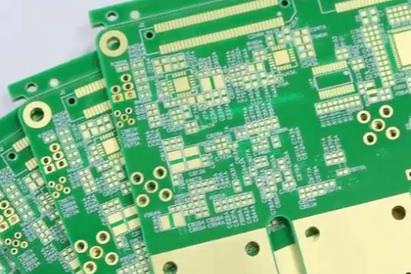
Circuit boards are more than just that green board in a phone
After years of working with RF and microwave circuit boards, I’ve learned that material selection can’t just rely on the numbers in the parameter sheet. Sometimes, the low-loss and low-Dk values advertised by manufacturers are completely different in actual applications. I remember our first collaboration with a certain RF and microwave PCB manufacturer; the material data they provided was impressively good, but the actual prototypes showed nearly 20% higher insertion loss in the high-frequency range than expected. We later discovered that their Dk stability fluctuated too much with temperature changes, causing a complete breakdown of impedance matching. This fluctuation was particularly noticeable in the -40℃ to +85℃ temperature range, especially in the frequency range above 10GHz, where a Dk change rate exceeding 50 ppm per degree Celsius would cause significant phase distortion. When we later performed swept-frequency tests with a vector network analyzer, we observed periodic jitter in the S21 parameter during temperature cycling, which directly affected the bit error rate performance of the communication system.
Truly reliable RF PCB manufacturers understand that material selection needs to be combined with specific application scenarios. Last year, we had a millimeter-wave radar project that used a microwave PCB material recommended by a small manufacturer. Initially, all indicators met the requirements, but after less than a week of operation in a low-temperature environment, the phase consistency showed serious drift. Upon inspection, we found that the dielectric constant of the board material drifted significantly due to moisture absorption. This lesson has taught me that I now always require suppliers to provide Dk change curves at different temperatures and humidity levels when selecting materials. For example, as relative humidity increases from 30% to 90%, the Dk value of some PTFE substrates can change by more than 8%, while hydrocarbon resin materials exhibit much lower moisture sensitivity. We now pay particular attention to material aging data under 85℃/85%RH conditions for 168 hours, which is crucial for high-reliability applications such as automotive radar.
Many people fall into the trap of pursuing extremely low loss. In fact, for most civilian RF applications, moderate dielectric loss can lead to better cost control. I’ve seen too many teams insist on using top-tier PTFE materials for consumer electronics, only to end up with dismal yields due to processing difficulties. The truly smart approach is to flexibly choose materials based on the frequency range. For example, modified epoxy resins are sufficient for IoT devices below 2.4GHz, balancing performance and cost, while ceramic-filled PTFE is only necessary for the 5G millimeter-wave band. Taking FR-4 material as an example, its loss tangent at 1GHz is approximately 0.02, which is higher than Rogers 4350B’s 0.0037. However, considering that the former costs only 1/5 of the latter per square meter, it is perfectly adequate for Bluetooth devices with transmission distances of less than 10 meters. We conducted comparative tests, and using FR-4 material for PCBs in the 2.4GHz band resulted in an overall link loss increase of no more than 1.5dB, but the BOM cost could be reduced by more than 40%.
During recent testing of a domestic RF board material, we made an unexpected discovery: although its nominal loss factor was slightly higher than imported materials, the smoother surface treatment of the copper foil actually reduced conductor loss by half a dB in actual array assembly. This reminds us that when evaluating PCB performance, we must move beyond simply looking at individual parameters. After all, electromagnetic waves propagate in a three-dimensional structure, and the interface characteristics between the substrate and copper foil are sometimes more important than the material itself. This domestic material uses reverse-treated copper foil, with a surface roughness Rz value controlled to within 1.8μm, while conventional rolled copper typically has an Rz of around 3.5μm. In 28GHz band testing, this smoother copper foil surface significantly reduced the additional loss caused by the skin effect, particularly improving the edge field of microstrip lines. We also found that its copper foil peel strength reached 1.2 N/mm, which is 30% higher than the industry standard, significantly improving the reliability of multilayer boards after lamination.
Ultimately, choosing RF/microwave PCB materials is like compounding traditional Chinese medicine; it’s useless to only focus on the efficacy of a single ingredient. You need to consider the synergistic effect of all components. My current habit is to conduct three sets of comparative experiments for each new material I encounter: insertion loss comparison at different line widths, phase stability after thermal cycling, and, most importantly, impedance consistency after multilayer board lamination. This real-world data is far more reliable than the theoretical values in the specifications. We pay particular attention to the transmission loss differences of three typical line widths: 0.1mm, 0.2mm, and 0.3mm, which reflects the material’s suitability for fine lines. In thermal cycling experiments, if the phase change exceeds 3 degrees after 100 cycles from -55℃ to +125℃, the material will be excluded from high-speed SerDes applications. By fabricating 8-layer test samples, we can simultaneously verify the material’s thermal expansion coefficient matching and lamination process window. These dynamic parameters are often more valuable than static Dk/Df values.
I’ve seen many engineers overly reliant on simulation software when designing RF/microwave PCBs. They spend a lot of time adjusting parameters in those 3D models—from dielectric thickness to copper foil roughness—but ignore the variables in actual production.
When collaborating with RF PCB manufacturers, I discovered an interesting phenomenon: what truly determines performance are often the details that simulation software cannot fully model. For example, the same design drawings given to different manufacturers result in significantly different boards.
Once, we tested two microwave PCB boards with different process treatments, and the differences were significant. One board had a smoother copper foil surface treatment, resulting in nearly 15% lower loss at high frequencies. This difference made me realize that the material’s inherent characteristics are more important than we imagined.
Many people think that everything will be fine as long as the impedance is calculated correctly, but it’s not that simple. Line width tolerance control introduces many variables in actual production; sometimes a 0.1 mm difference in the design value can worsen the standing wave ratio across the entire frequency band. I prefer working with RF PCB manufacturers who are willing to communicate details, as they proactively provide feedback on issues encountered during production, such as the actual control capabilities of sidewall verticality during the etching process. These are often more valuable than theoretical parameters.
I remember a project where we repeatedly adjusted the transmission line structure during the design phase, trying to replace some passive components with distributed parameters. However, we found that the stability of the actual product was far inferior to using high-quality surface-mount components. Sometimes, excessively pursuing theoretical perfection can lead to new problems.
Now, when designing RF PCBs, I tend to treat simulation results as a reference direction rather than an absolute standard. After all, the actual propagation characteristics of electromagnetic fields are affected by too many factors, from material batch variations to the temperature and humidity of the production environment.
A good RF microwave PCB manufacturer should be able to tell you their process limitations, such as the minimum line width they can achieve and the range within which they can control the uniformity of the dielectric thickness. This kind of real-world production data is far more reliable than any simulation results.
I recently chatted with an antenna engineer and discovered an interesting phenomenon – their team went through three RF microwave PCB manufacturers before finding a suitable partner. Either the board material parameters didn’t meet the specifications, or delamination and blistering problems occurred during soldering. This reminded me of a point often overlooked in the industry: even the most perfect simulation model has to compromise with manufacturing processes.
I remember a millimeter-wave radar project I participated in last year that failed because of the waveguide structure. Theoretically, using low-loss materials should achieve a transmission loss of 0.2 dB, but the actual test showed a loss of 0.8 dB. Later, disassembly revealed that resin flow during the lamination process caused a 3-micron deviation in dielectric thickness – this error is insignificant in low-frequency circuits, but it directly caused the standing wave ratio to collapse at 77 GHz. Some RF PCB manufacturers always talk about dielectric constant stability but rarely mention whether their prepreg matching scheme can truly control the Z-axis expansion coefficient.
The true test of a microwave PCB manufacturer’s capabilities lies in their attention to detail. For example, a deviation of more than 50 microns in the position of the metallized vias in a grounded coplanar waveguide will cause the electromagnetic field distribution to deviate. I’ve seen people use laser marking machines to make positioning marks on the board material, which actually introduces new dielectric non-uniformity. The truly professional approach is to lock the fiber direction through an optical positioning system during the material cutting stage. Many teams are blindly pursuing ultra-low-loss materials but neglecting a crucial fact: beyond a certain critical point of low loss, the key to improving signal integrity becomes impedance continuity. In one test, a certain brand of hydrocarbon ceramic substrate showed Dk value fluctuations of up to 0.2 between different batches, leading to a cumulative phase error of 15 degrees in the microstrip lines. This kind of deviation is disastrous in phased array systems.
When choosing an RF/microwave PCB supplier, I value their engineering responsiveness more than the parameters listed in their brochures. Good manufacturers can tell you why stripline structures have lower actual losses than microstrip lines in certain frequency bands. They even have their own compiled dielectric loss tangent temperature drift curves, and this data is often closer to real-world scenarios than standard values. After all, in the high-frequency world, there are a hundred process pitfalls between theoretical and achievable values.
I’ve been involved in the field of RF/microwave PCBs for several years. Many people think this stuff is very mysterious and far removed from daily life. That’s not true. The cell phone base stations you use every day, and the Wi-Fi routers in your home, all rely on these components. They are like highways in the world of circuits, specifically responsible for transporting those invisible, intangible high-frequency signals. The quality of these “highways” directly affects how fast and stable the signals travel.
Traditional PCB boards are more like country roads, fine for low-frequency signals. But once the frequency increases, various problems arise. Signals reflect, attenuate, and even interfere with each other. This is where specialized RF PCBs come in. They need to consider not just simple on/off issues, but how to make electromagnetic waves obediently follow a designated path.
I’ve seen many projects fail due to material selection. Some people used ordinary FR4 material for RF boards to save money, resulting in terrible performance. High-frequency signals are particularly sensitive to dielectric loss. This is like driving a sports car on a muddy road; even the best engine won’t perform well. For example, in 24GHz automotive radar applications, the loss tangent of ordinary FR4 can be as high as 0.02, while specialized high-frequency boards can keep it below 0.004, meaning the signal transmission distance can be increased by more than 30%. Finding a reliable RF/microwave PCB manufacturer is crucial; they understand the intricacies and know when to use Rogers and when to use Taconic materials. These specialized materials not only have stable dielectric constants, but their thermal expansion coefficients perfectly match those of copper foil, ensuring stable electrical performance across an extreme temperature range of -55℃ to 125℃.
The design phase is where expertise is truly tested. Minute differences in parameters like trace width and dielectric thickness can lead to vastly different performance. For example, in the millimeter-wave band, a transmission line width error exceeding 0.1 mil can cause a characteristic impedance change of more than 5%, directly leading to signal reflection. Designers must calculate the electromagnetic field distribution with the precision of a watchmaker, even considering the additional capacitance caused by conductor edge effects.
I remember once debugging a 2.4GHz power amplifier module where the entire matching network failed because the ground via was misplaced by half a millimeter. Later, 3D electromagnetic simulation revealed that this tiny offset altered the ground current path, changing the actual electrical length of the microstrip line, which was originally designed to be λ/4. This level of precision is equivalent to accurately locating a sesame seed on a football field.
The biggest mistake in RF PCB design is simply applying digital circuit design principles. Digital circuits are concerned with the transitions between 0 and 1, while RF circuits focus on the complete waveform of each sine wave. For example, power decoupling capacitors, which can be placed arbitrarily in digital circuits, must be carefully positioned in RF circuits; otherwise, the capacitor lead inductance will resonate with the capacitor itself.
You must always remember that you are dealing with electromagnetic waves, and they have their own characteristics. Electromagnetic waves propagating in transmission lines exhibit the skin effect, causing current to concentrate on the conductor surface. At 10GHz, the skin depth is only 0.66 micrometers, requiring PCB surface treatment to use a smoother chemical gold plating process instead of ordinary tin plating.
Impedance matching is a classic example; 50 ohms wasn’t chosen arbitrarily. It’s a compromise between power handling capacity and loss. Research from the time of coaxial cable invention showed that 30 ohms provided the maximum power handling capacity, 77 ohms provided the minimum loss, and the geometric mean resulted in 53 ohms, which was eventually standardized to 50 ohms. This value ensures both power transmission efficiency and ease of connector manufacturing.
Some beginners like to cram as many components as possible onto the board, thinking that more is better. However, high-frequency circuits prioritize simplicity, as each component introduces parasitic effects. A 0805 surface-mount capacitor, at 5GHz, exhibits a parasitic inductance of approximately 0.8nH, which is enough to transform a capacitor intended for filtering into a band-pass filter. Once, we improved the efficiency of a power amplifier by 12% simply by removing two redundant matching capacitors.
The testing phase is even more challenging. A network analyzer alone isn’t enough; you need to know how to interpret the S-parameter curves. I once stayed up for three nights straight trying to understand a strange dip in the insertion loss curve at 5GHz, only to discover that the microstrip line bend angle was too sharp. In fact, when the bend angle is less than 135 degrees, the corner acts as a parallel capacitor. If the line width is 20 mil, this parasitic capacitance can reach 0.02pF, causing a significant signal resonance point at 5GHz.
The most interesting aspect of this industry is the close integration of theory and practice. Even the most powerful simulation software cannot replace actual debugging. A perfect ideal model in simulation is affected by dozens of variables in reality, including PCB manufacturing errors, material anisotropy, and soldering temperature. Once, a simulation showed a perfect -20dB return loss, but the actual measurement was only -12dB. It turned out that the lamination process caused uneven dielectric layer thickness.
Many manufacturers are now pursuing higher-frequency solutions, and the application of millimeter-wave bands is becoming increasingly widespread, placing more stringent demands on microwave PCBs. In 77GHz automotive radar, the wavelength is only 3.9 millimeters, requiring the transmission line edge roughness to be less than 0.1 micrometers; otherwise, the signal will scatter severely, as if reflecting off a sandpaper surface.
Materials need to be more stable, and manufacturing precision needs to be higher; sometimes, even the surface roughness of the copper foil can be a decisive factor. Currently, advanced low-profile copper foils can control surface profile height to within 0.5 micrometers, reducing conductor loss by 70% compared to traditional copper foils. In the 60GHz band, this improvement can nearly double the signal transmission distance.
However, the more challenging the technical breakthrough, the greater the sense of accomplishment. When you see the beautiful curves your designed RF board produces on the spectrum analyzer, that feeling of satisfaction is something no other project can provide. Especially when the vector network analyzer displays a flat group delay curve, or the noise figure tester shows a noise figure below 1dB, that feeling of precisely controlling electromagnetic waves is like a conductor perfectly leading an entire symphony orchestra.
After working in the RF field for a while, you’ll notice an interesting phenomenon—many people think that simply connecting the circuit will make the signal work. In reality, high-frequency signals are far more sensitive than we imagine. I remember once testing a microwave frequency module and finding a particularly large signal attenuation. After much investigation, I discovered that the dielectric constant of the PCB material was drifting at high temperatures.
Now, many RF and microwave PCB manufacturers are starting to focus on the thermal stability of materials. Especially when equipment needs to operate outdoors or in high-temperature environments, ordinary FR4 materials simply can’t withstand the conditions. I’ve seen some RF PCBs used in base stations that even need to consider performance under direct sunlight; this is where the advantages of ceramic substrates or special composite materials become apparent. Taking Rogers Corporation’s RO4000 series high-frequency laminates as an example, their dielectric constant temperature coefficient can be controlled to within -50 ppm/°C, far superior to the 200-300 ppm/°C fluctuation range of ordinary FR4 materials. In 77GHz automotive radar applications, this stability directly relates to the consistency of millimeter-wave phase, which in turn affects the accuracy of target detection.
The impact of packaging methods on high-frequency circuits is often underestimated. Traditional QFN or BGA packages are fine at low frequencies, but once you enter the microwave frequency range, the parasitic parameters of the package pins become performance killers. I recently encountered a solution using embedded packaging, where the RF chip is directly embedded in the PCB dielectric layer, and the effect is indeed excellent. This solution reduces the bond wire length from the traditional 1-2mm to a few micrometers, reducing insertion loss by approximately 0.3dB in the Ka band (26-40GHz), while controlling the package inductance to below 0.1nH. However, this technology requires precise control of the thermal expansion coefficient matching between the chip and the dielectric layer; otherwise, delamination can easily occur during temperature cycling tests.
When choosing a PCB supplier, I particularly value whether they truly understand electromagnetic field characteristics. I once encountered a supplier who could produce fine lines but was vague in their explanation of impedance control; such collaborations are very difficult. Good RF PCB manufacturing requires engineers who understand both the manufacturing process and electromagnetic theory. For example, when designing grounded coplanar waveguides, it’s necessary to consider both the impact of conductor surface roughness on the skin effect and the nonlinear characteristics of the dielectric loss tangent as a function of frequency. Excellent engineers will optimize the field distribution at the edge of the conductor strip through 3D electromagnetic field simulation, rather than simply relying on empirical formulas.
Regarding future trends, I believe flexible microwave PCBs will become increasingly important, especially in wearable devices and automotive radar applications, where circuits need to adapt to various curved structures. This presents new challenges for both materials and manufacturing processes. Currently, polyimide-based flexible circuits still face significant loss issues at frequencies above 40 GHz, while liquid crystal polymer materials, although exhibiting excellent high-frequency characteristics, still have immature multi-layer lamination processes. Some laboratories are attempting to deposit aluminum nitride thin films on flexible substrates to improve thermal management, which is crucial for the bending reliability of 5G millimeter-wave antenna modules.
Sometimes I feel like working in RF is like playing hide-and-seek with electromagnetic waves; you never know where the next problem will appear. But it’s this uncertainty that makes this field so fascinating; solving each new problem feels like unraveling a natural mystery. For example, when debugging a 28 GHz phased array system recently, we discovered a periodic deviation in beam pointing, which was ultimately traced back to the coupling effect between the ESL parameter of the power supply filtering capacitor and cavity resonance. This kind of cross-disciplinary troubleshooting often requires considering the interaction of multiple physical domains, including circuits, electromagnetic fields, and thermodynamics.
I’ve been working in this industry for over a decade and have observed an interesting phenomenon: many people, when discussing RF and microwave PCBs, are quick to focus on sophisticated simulation software. However, what truly determines success or failure are often seemingly basic material selection issues. Take transmission lines, for example. We once took on a project where the client specifically emphasized using the lowest-loss solution. However, the test data from the first batch of boards was completely wrong. We later discovered the problem lay in the seemingly insignificant copper foil treatment. The so-called low-roughness copper foil provided by the supplier simply didn’t meet the requirements for high-frequency applications. That lesson taught me a valuable lesson: finding a reliable RF and microwave PCB manufacturer is more important than anything else. They know what kind of surface treatment truly controls losses, rather than just relying on theoretical concepts. For example, the contour shape of copper foil affects the skin effect, and the surface roughness produced by different rolling processes results in completely different phase responses in the millimeter-wave frequency band. These details are often only accurately understood by experienced manufacturers.
I’ve seen too many engineers spend time designing various complex via structures while neglecting the most basic material matching issues. Once, when testing microwave PCBs from different manufacturers, we found that the loss difference for the same design on different materials could reach over 20%, which is quite astonishing, especially when you need to transmit signals over long distances. Even small differences in loss can be amplified into serious problems. So now I’ve developed a habit of confirming the manufacturer’s material inventory and actual performance parameters before starting a new project, rather than simply trusting the nominal values in the datasheet. For example, we compared three different brands of PTFE substrates, and the dielectric constant fluctuated by 0.2 at 40GHz, which directly led to deviations between the actual electrical length of the microstrip line and the design value.
The testing phase cannot be taken lightly either. Many people think that the S-parameters measured by a vector network analyzer are the final answer, but there are many subtleties involved. For example, different calibration methods can lead to significant differences in results. Our team once built a completely new testing environment specifically for a millimeter-wave project to ensure the accuracy of the measurement results. During that time, we spent almost every day in the lab, repeatedly comparing data changes under different conditions. Although this process was arduous, it did give us a deeper understanding of the performance of RF PCBs. Looking back now, all those late nights were worth it. In particular, during the probe station calibration process, we found that even using the same calibration substrate, differences in probe pressure applied by different operators could lead to a 0.1dB fluctuation in measurement repeatability.
Speaking of grounding via design, I think many people fall into the trap of over-design, always pursuing the highest possible via density. But in reality, the key is to ensure the quality of the via fabrication. We encountered a situation where the via spacing specified in the design file was perfect, but the actual fabrication resulted in new problems due to limited process capabilities. Therefore, I now prefer to communicate fully with the manufacturer to understand their actual processing capabilities before deciding on the final design solution. This pragmatic approach often leads to better results. For example, some manufacturers have poor control over the uniformity of copper plating on the walls of holes with diameters below 0.2mm, and blindly pursuing high density can lead to reduced grounding reliability. My perspective on back-drilling technology might be a bit different. While it can indeed solve the stub effect, it’s not necessary in all situations, especially for applications with relatively low frequencies. Sometimes, simple design optimizations can achieve similar results, and back-drilling adds significant costs. These factors need to be weighed against specific requirements. I generally advise clients to conduct thorough simulations and verification before deciding whether to adopt such a complex process. After all, good engineering practice should prioritize simplifying the design while still meeting performance requirements. For example, in frequency bands below 28GHz, optimizing via anti-pad dimensions and using stepped impedance matching can often achieve performance comparable to back-drilling.
Finally, I want to say that what this industry lacks most isn’t advanced technology, but a pragmatic attitude. Too many people are eager to chase the latest technologies and processes, neglecting the most basic engineering principles. I’ve seen too many projects fail not because the technology wasn’t advanced enough, but because the fundamental work wasn’t done properly. That’s why when I lead a team, I emphasize the importance of mastering the basics. Whether it’s material selection or testing and verification, everything needs to be done step by step, thoroughly and meticulously. For example, we require every new engineer to personally complete the entire process from board cutting to vector network analyzer calibration. This seemingly clumsy training method allows young engineers to quickly build a solid foundation.
I recently had a conversation with a friend who works in communication equipment, and I discovered an interesting phenomenon. Many engineers are overly focused on the numerical indicators in the technical parameter sheets when choosing RF microwave PCB suppliers. I think those cold, hard numbers are just the basic threshold.
What truly determines the success or failure of a project is often something more practical. For example, when our lab needed to make a batch of 77GHz automotive radar boards, we compared three suppliers. The first one provided a very impressive material parameter sheet, but they couldn’t even achieve basic impedance matching during prototyping. The second one had high process precision, but their engineers couldn’t understand our specific requirements for phase consistency. We eventually found our current partner; their biggest advantage is that they can send engineers to directly participate in our early design discussions.
Many people may not realize that the most difficult part of RF PCB manufacturing isn’t the manufacturing itself, but how to accurately convey the design intent to the production process. Once, we designed a multi-layer hybrid board structure; theoretically, the simulation data was perfect, but the manufacturer, due to insufficient understanding of the characteristics of PTFE material, caused tiny air bubbles to appear between the layers during the actual lamination process. This kind of problem can’t be identified simply by looking at the equipment list; the key is whether the manufacturer has practical experience in handling similar structures.
I place great importance on whether the supplier’s engineering team can quickly understand our needs. Sometimes the performance requirements we propose may sound a bit idealistic, but a good manufacturer will proactively help us analyze which indicators can be achieved through process optimization and which require design adjustments. This kind of interaction is far more meaningful than simply comparing prices.
There’s a misconception in the industry right now: an overemphasis on the brand effect of high-frequency materials. In fact, even with the same Rogers material, the RF performance can vary significantly depending on the manufacturer. The key is whether they have established their own process database and can adjust processing parameters based on the material characteristics. We’ve encountered situations where using top-tier materials resulted in higher losses than with ordinary materials.
Regarding testing, many manufacturers claim to provide S-parameter testing, but the actual implementation varies greatly. Some simply measure a few frequency points, while others can provide complete frequency response curves and even performance stability data under temperature variations. These details often reflect the manufacturer’s level of professionalism.
I think choosing an RF/microwave PCB manufacturer is like finding a partner. Technical capability is just the entry ticket; more importantly, it’s about whether they are willing to spend time understanding your project needs and proactively proposing solutions when problems arise. After all, even the most perfect technical specifications are no match for a supplier who can work alongside you.
Circuit boards are more than just that green board in a phone
From disassembling old routers to visiting electronics manufacturing plants, I gradually realized
As an electronics enthusiast, I’ve come to understand firsthand the impact of
- Expert på produktion av små till medelstora serier
- Kretskortstillverkning med hög precision och automatiserad montering
- Pålitlig partner för OEM/ODM-projekt inom elektronik
Öppettider: (mån-lör) från 9:00 till 18:30