

What Documents Are Required for PCB Production: A Field Guide From Real Industrial Weighing Controller PCB Projects
Many engineers focus too much on technical parameters early on and overlook
RF Filter PCB Design: Why Layout Outranks Material Choice Every Time
RF circuit design carries a reputation as engineering’s closest approximation to mysticism. That reputation is partially deserved. A two-month engagement with a single PCB trying to achieve the specified out-of-band rejection for one project did something to change the initial framing. The analogy that eventually felt accurate: every layer of material and every trace on the board collectively determines whether you receive a clean signal or an undifferentiated noise floor. The effort to distinguish those two outcomes in practice is unglamorous and systematic.
The observation that generates most confusion in discussions of RF filter PCB design is the presumption that material selection is the primary determinant of performance. It is not.
The Parasitic Zoo
A simple low-pass filter contains the following elements that appear nowhere on the schematic: the capacitance between each trace and the reference plane, the inductance of each trace segment, the mutual coupling between adjacent traces, and the capacitance introduced by each via transition. These are the parasitic elements — the zoo of unintended reactive components that every physical implementation of a filter circuit produces.
A textbook three-pole Chebyshev filter computed to have a corner frequency of 3.5 GHz may exhibit a spurious transmission path near 2 GHz in its physical implementation. The mechanism is parasitic coupling between input and output sections of the filter — a path that does not exist on the schematic, created by the physical proximity of traces on a dielectric medium. The filter passes interference at a frequency it was designed to reject. No amount of premium substrate material closes that unintended path. Only layout change eliminates it.
The implication is direct: design topology and layout must precede material selection in the design sequence. Define the electrical performance requirements. Determine which circuit topology can achieve them. Understand which layout configurations minimize parasitic coupling for that topology. Then select a substrate material whose physical properties — dielectric constant, loss tangent, dimensional stability — can support that layout without introducing additional limitations.
Reversing this sequence — selecting an expensive material first and then attempting to design around its properties — produces suboptimal results at elevated cost.
Material Selection in Proper Proportion
Dielectric constant stability is genuinely important at high frequencies. Small variations in the substrate’s dielectric constant produce small variations in the physical dimensions required for a given electrical characteristic. In precision filter applications, particularly those operating above a few gigahertz, accumulated dimensional sensitivity from material variation can shift the filter response enough to violate the specification. This is the legitimate argument for high-stability substrate materials.
Loss tangent matters for insertion loss and quality factor. A lower loss tangent substrate enables sharper filter rolloff for a given resonator geometry, because the resonator Q is higher. At frequencies above a few gigahertz, the difference between a 0.001 loss tangent material and a 0.005 material is measurable in filter selectivity.
But material selection should match the application. A filter for a consumer wireless product operating at 2.4 GHz has different requirements than a filter for a base station transmitter operating at 28 GHz. The materials appropriate for the second application carry significant cost and handling overhead that is not justified for the first. Engineering judgment about where the material properties actually constrain performance is more useful than defaulting to the most expensive available option.
Coupled Resonator Geometry: Where Theory Meets Physical Reality
A hairpin filter — two parallel resonator sections coupled by proximity — illustrates the gap between theoretical and physical performance directly. The coupling coefficient between the sections depends on their separation, their lengths, and their interaction with the reference plane. Standard design equations provide a starting estimate. The physical implementation typically requires measurement and tuning because the equations assume ideal conditions that the fabricated structure does not provide.
Stub elements added to control bandwidth contribute their own parasitic parameters. The open or short circuit stub interacts with the main resonator through fields that extend beyond the stub’s physical boundaries. If the design procedure treats the stub as an ideal lumped element rather than a physical distributed structure, the fabricated filter’s center frequency will differ from the simulated prediction. The magnitude of the discrepancy depends on frequency and geometry — at lower frequencies it may be negligible; at millimeter-wave frequencies it may be several percent of the center frequency, which is a significant problem for narrow-bandwidth designs.
Proximity effects between resonators create coupling paths that simulation may not capture fully. When two resonators are arranged to achieve a target coupling coefficient, unintended coupling through other field paths can create additional filter poles or zeros that distort the response. These effects become more pronounced as resonator Q increases — which means that high-quality substrate materials can actually make parasitic effects more visible, not less, because they propagate the unwanted field components more efficiently.
The Manufacturing Process Factor
The gap between a well-simulated filter and a well-performing fabricated filter frequently traces to manufacturing process variables that ideal simulation models do not represent.
Metal conductor surface roughness increases effective insertion loss at high frequencies through the skin effect. Simulation assumes smooth conductor surfaces. Real etched copper has surface texture at the micron scale. The additional loss from surface roughness is frequency-dependent — it becomes a meaningful fraction of total insertion loss at millimeter-wave frequencies even when it is negligible at lower frequencies.
Prepreg resin flow during lamination creates local variation in dielectric layer thickness. Simulation assumes uniform dielectric constant throughout the substrate volume. Where resin has flowed non-uniformly during pressing, the local dielectric constant departs from the nominal value. The result is distributed impedance variation that degrades the precision of resonator tuning.
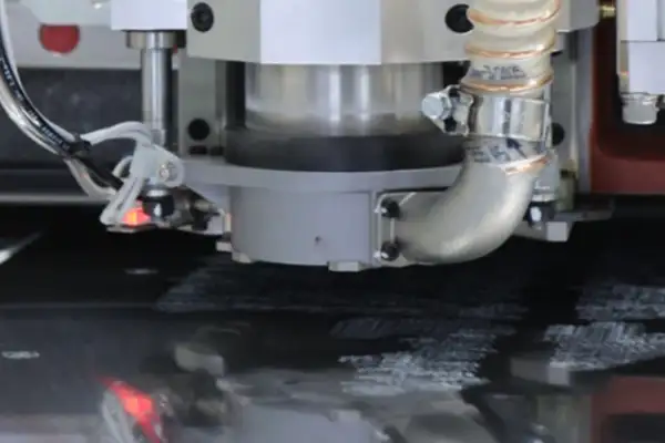
Via hole processing affects performance through drill debris and plating quality at the via wall. For high-frequency materials — Rogers, Taconic, and similar substrates — the mechanical processing requirements for hole formation differ from FR4. Inadequate plasma cleaning or chemical desmear after drilling leaves residue at the via wall that degrades plating adhesion and increases via resistance. For phase-sensitive filter structures, via resistance variation across the board introduces phase errors that shift the frequency response.
These manufacturing variables are not visible in the final product by visual inspection. They are revealed through RF measurement of production samples and through statistical analysis of yield variation. A supplier who has invested in understanding how their specific process parameters affect high-frequency circuit performance — and who can discuss the relationship between their process control methods and the RF outcomes — has engineering depth that equipment lists do not capture.
Evaluating Suppliers for RF Filter Work
The evaluation framework that applies to high-volume commodity PCB production does not transfer directly to RF filter board manufacturing. Equipment specifications establish a baseline. The differentiation lies in process understanding and engineering engagement.
A capable supplier evaluates the customer’s design files for RF-specific risks before committing to production. Via placement relative to RF structures, ground plane continuity beneath high-frequency traces, and trace geometry effects on characteristic impedance are examples of issues that an experienced RF PCB engineering team identifies at design review rather than discovers at measurement. Suppliers who provide this kind of pre-production design feedback reduce iteration cycles — which reduces project schedule and cost more than material selection optimization does.
Materials management for high-frequency substrates is a process discipline, not a purchasing decision. The correct questions to ask a supplier about material management: what is the storage humidity and temperature specification for the materials you use for RF boards? How do you track lot-to-lot dielectric constant variation, and what is the acceptable range before you adjust process parameters to compensate? How do you handle material that has been in storage longer than the manufacturer’s specified shelf life? Answers that demonstrate actual process controls — not just assertions that the material meets specification — indicate a supplier who understands what they are managing.
The relationship between material consistency and production yield at RF frequencies is not linear. A supplier who achieves consistent results with materials characterized as “second tier” by nominal specification may produce more reliable filter performance than one who uses top-specification materials without the process discipline to extract their potential. The specification sheet value of dielectric constant is a nominal number. The value that affects your filter is the actual value in the specific lot processed through the specific lamination cycle on a specific day. A supplier who knows the difference between these two numbers and manages toward the second one is the supplier who produces consistent RF results.
The final point concerns production capacity alignment. A supplier who successfully completed millimeter-wave antenna array work for one customer may not have the engineering attention available for a small-volume, high-precision filter project if their capacity is dominated by large-volume orders. Production resource allocation — not equipment capability — determines whether your project receives the engineering engagement that RF filter development requires. Understanding the supplier’s current project mix and their bandwidth for technically demanding work is as important as understanding their technical capability statement.
Many engineers focus too much on technical parameters early on and overlook
As someone who has worked in PCB outsourcing for years, I’ve found
Cramming a camera, amplifier, dual-mic array, and Wi-Fi radio into a palm-sized
- Expert på produktion av små till medelstora serier
- Kretskortstillverkning med hög precision och automatiserad montering
- Pålitlig partner för OEM/ODM-projekt inom elektronik
Öppettider: (mån-lör) från 9:00 till 18:30
Get quote, solution or any question, Andre always here to help