
How to Choose an Excellent Semiconductor Flex PCB Manufacturer?
While collaborating with a smart wearables team to select a semiconductor flex
Every time I receive a bare, unpopulated PCB, I feel a mix of excitement and nervousness—this thing is, after all, the skeleton of the entire electronic product.
I’ve seen plenty of people, when prototyping, simply grab a generic prototype board and start piling components onto it. In reality, however, the design of the Bare PCB is where an engineer’s true technical chops are put to the test.
I recall an instance where I helped a friend debug a sensor module that was constantly acting up. At first, we both assumed the problem lay with the software code or the sensor itself.
Eventually, having exhausted all other options, we disassembled the entire module to inspect it closely. The result? We discovered a subtle issue with the trace spacing on that custom-designed bare board.
This experience made me realize that, quite often, the root of a problem lies hidden within the most fundamental elements of a system.
Nowadays, whenever I undertake a new project, I place a strong emphasis on the PCB design phase. After all, even the best components are useless if they are soldered onto an unreliable foundation. Some people argue that using off-the-shelf prototype boards saves both time and money. Indeed, for simple experiments or educational demonstrations, these generic boards are quite convenient. However, if your goal is to produce a truly reliable product, you simply must start with a custom-designed bare board.
I like to liken the Bare PCB to the foundation of a building—you may not always see it, but it is what ultimately determines the stability of the entire structure.
The smart home controller I’ve been working on recently serves as an excellent example of this principle. To ensure signal integrity, we dedicated two full weeks solely to the PCB layout design. Although this required a greater upfront investment of time, it resulted in an incredibly smooth and trouble-free debugging process later on. There is a profound sense of assurance that comes from knowing you’ve maintained full control over the project right from the foundational level.
And every time I hear someone talk about Bare PCBs as if they were some sort of mystical, magical artifact, I can’t help but chuckle. It often seems as though you could just grab any bare PCB off the shelf and use it to complete any project. In reality, however, selecting the right board is far more complicated than one might imagine—especially once you actually roll up your sleeves and get to work.
I certainly made my share of rookie mistakes back when I was first getting into electronics design. I naively assumed I could just find a cheap supplier, order a few random boards, and use them for testing. The moment the first batch of bare PCBs arrived, however, I discovered that the pads were severely oxidized. It was only then that I realized you simply cannot choose bare PCBs based on price alone. Some suppliers sound incredibly accommodating when they advertise “no minimum order quantity,” but what they actually ship you might be nothing more than old, stagnant stock from a previous production run.
Nowadays, whenever I deal with suppliers, I make a point of asking for specific details regarding the source of their board materials and their storage conditions—especially for high-frequency projects. Even during the prototyping phase, I insist that they use vacuum packaging. I once encountered a particularly stubborn supplier who adamantly claimed that a standard anti-static bag would suffice. The result? When the boards finally arrived, the signal attenuation was so severe that the data was completely unrecognizable—utterly mangled. Dealing with such details can truly drive a person insane.
What I fear most, however, are those suppliers who make wildly exaggerated claims. They’ll immediately bombard you with a stack of certification certificates, yet when it comes time for mass production, they can’t even consistently maintain basic impedance control. I now prefer to work with manufacturers who are honest enough to admit the limitations of their processes. At the very least, they know when to say, “Sorry, we can’t do that.” Compared to those who blindly accept every order that comes their way, these honest manufacturers are far more worthy of a long-term partnership.
I’ve recently been helping a friend with a small-batch production run for an automotive sensor project. We solicited quotes from five or six different suppliers and noticed an interesting phenomenon: while some manufacturers quoted a higher unit price per board, they actually turned out to be the more cost-effective choice once engineering fees and revision costs were factored in. This is especially true when you need to fine-tune trace widths and spacing; professional manufacturers have a significantly higher probability of getting it right on the very first attempt.
Ultimately, choosing a bare PCB supplier is a lot like choosing a spouse: you can’t base your decision solely on appearances. You have to go through a period of “trial and error”—a process of mutual adjustment—to determine whether you’re truly a good match. My current strategy is to allocate a specific budget for “trial and error” for every new project. I start by ordering small batches from two or three different suppliers to test the waters, then compare the actual soldering yield and signal integrity of each batch. While this means spending a few extra thousand dollars on testing fees upfront, it’s infinitely better than facing a total write-off of the entire production run during mass manufacturing.
I recall an instance at a trade show where I met a Taiwanese supplier who was incredibly straightforward and honest. He openly admitted that their standard FR4 board material was unsuitable for millimeter-wave frequency applications, and he even went so far as to recommend a different manufacturer specializing in ceramic substrates that would be a much better fit for my needs. That very candor actually led me to transfer all of our company’s prototype orders to them later on. A good supplier should act more like a technical consultant than just a vendor selling circuit boards.
Ultimately, the most important rule in the electronics industry is this: don’t be tempted by rock-bottom prices. Those who advertise “ultra-low” minimum order costs often have hidden pitfalls lurking beneath the surface. After all, manufacturers need to make a profit, too. When a price seems unreasonably low, you have to ask yourself where exactly they managed to cut corners to achieve it.
Oh, speaking of storage conditions, I almost forgot to mention something: during last year’s rainy season, a batch of bare PCBs in our warehouse absorbed moisture, resulting in delamination and cracking. Consequently, we now require that all bare PCBs undergo a drying process before being placed into storage. That lesson cost us over 100,000 in scrapped inventory. Nowadays, whenever I see someone carelessly stacking bare boards inside cardboard boxes, it makes my skin crawl. Whenever I see a bare PCB lying on my workbench, I’m always struck by how deceptive it actually is. On the surface, it looks like nothing more than a green or brown board crisscrossed with lines; yet, its true value lies entirely in the components that have yet to be mounted upon it.
When I first started working with hardware, I, too, was under a misconception: I thought that simply soldering a bunch of impressive chips, resistors, and capacitors onto a board was all it took to get the job done. It was only later that I realized if the circuit board serving as the foundation for these components is unreliable, even the finest components are rendered useless. It is much like building a house: if the foundation isn’t laid securely, no matter how expensive the interior finishes you use, the house is bound to collapse regardless.
Take, for instance, a small project I worked on last year. To save on costs, I selected a manufacturer that offered an exceptionally low quote for the bare boards. When the boards arrived, however, I noticed that the edges of the traces were rough and frayed, and there were several scratches—subtle enough to be easily missed by the naked eye. I didn’t give it much thought at the time, assuming these flaws wouldn’t affect functionality. It was only after I had soldered on all the electronic components and powered up the device for testing that I discovered severe instability in signal transmission. After weeks of troubleshooting, I finally traced the problem back to those very defects. I was forced to scrap the work and start over from scratch—a process that, ironically, ended up costing me far more in terms of time and resources.
Consequently, I now place immense importance on quality control during the bare-board stage. This step may appear simple, but it ultimately determines the success or failure of every subsequent stage. A high-quality bare circuit board—featuring crisp traces, a smooth surface, and uniform material consistency—can spare you a great deal of trouble down the road.
Many people believe that the “soul” of an electronic product resides in its gleaming chips. While that is certainly true, one must not forget that these “souls” require a stable and reliable physical vessel to truly fulfill their purpose. I have come to feel increasingly that the process of designing a circuit board and selecting components is akin to constructing an ecosystem; every part is interdependent and indispensable. And the bare PCB is the very place where this entire ecosystem begins.
Sometimes, gazing at a bare PCB before any components have been soldered onto it actually helps one quiet the mind and reflect on the overall soundness of the design. It is like a blank canvas waiting to be filled—holding within it every conceivable possibility, yet simultaneously serving as a test of the creator’s initial layout and planning skills.
Whenever I see those bare circuit boards lying on my workbench, I am reminded of the pitfalls I stumbled into during my early days. Many people assume that when purchasing bare PCBs, the only factor that matters is finding the lowest price—a notion that is incredibly naive. I have witnessed instances where someone chose the cheapest bare PCB available just to save a few pennies, only to discover during testing that the signal interference was so severe that the board was rendered completely unusable. In such a scenario, even the lowest procurement price becomes a complete waste, because you are forced to redesign and rework everything, effectively throwing away all the time and effort you invested.
The prototyping phase is precisely when you should be making your heaviest investments. I recall a project involving a four-layer PCB where we discovered an impedance mismatch issue during the very first prototyping run. Had we skipped that step and proceeded directly to mass production, the consequences would have been too disastrous to even contemplate.
Speaking of packaging, it’s a subject that often leaves me feeling a mix of amusement and exasperation. I once received a batch of vacuum-sealed prototypes, only to find upon opening them that the corners of the boards were completely shattered. I later realized that multi-layer PCBs require protection not only against physical shock but also against moisture; otherwise, humidity fluctuations during transit can cause the boards to warp.
During the design phase, many people tend to overlook the critical importance of proper layout partitioning. This is especially true for mixed-signal boards; if you cram the analog and digital sections too close together, the subsequent debugging process will give you such a massive headache that you’ll start questioning your career choices.
Regarding contracts, the clause I value most isn’t the pricing—it’s the one concerning intellectual property protection. I once dealt with a factory that secretly accepted private orders using our proprietary design files; had our contract not contained explicit, written compensation clauses, we would have had absolutely no legal recourse to defend our rights.
The logistics side of things is actually quite interesting. For prototypes, I always opt for air freight; although it’s more expensive, it allows me to receive the physical boards sooner and begin testing immediately. For large-volume orders, I switch to sea freight; the money saved is substantial enough to cover the cost of running two additional prototyping iterations. However, regardless of the shipping method, you must keep a close eye on the customs clearance documentation—particularly the Certificate of Origin. Missing even a single document can result in your shipment getting stuck in customs for up to two weeks.
The most important piece of advice I can offer newcomers is this: do not be lured in by rock-bottom prices. While they may appear to save you on upfront procurement costs, the hidden costs associated with subsequent repairs and rework can easily end up being double the original price. A high-quality bare PCB should serve as a solid foundation for your project; even if it costs a little extra, it is well worth the investment.
Whenever I see those bare, unpopulated circuit boards lying on my workbench, I find it absolutely fascinating. They serve as the skeletal framework of the electronic world—and paradoxically, without any components attached, the true essence of the design becomes even more apparent. For instance, by observing the routing paths of the power and signal lines, one can clearly discern how the designer intended to mitigate interference, and even anticipate potential thermal hotspots. This level of transparency makes the debugging process far more intuitive; particularly when using a multimeter to check for continuity, the state of the bare board provides a direct reflection of the underlying routing quality.
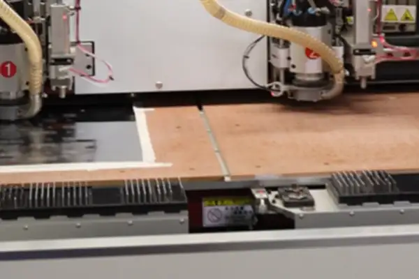
When I first started dabbling in electronics projects, I, too, stumbled down quite a few dead ends. I remember one instance where I spent ages searching for a suitable off-the-shelf development board for a simple LED control project, only to discover that none of the available options were the right size for my application. It wasn’t until later that I realized using a bare PCB directly was the correct approach all along. I ordered a few prototype boards from JLCPCB, and debugging them turned out to be incredibly smooth and effortless. During the actual soldering process, I discovered that the placement of the reserved test points was very well-thought-out, saving me the hassle of having to run extra flywires. This kind of customized experience made me realize that, during the transition from schematic to physical board, the size and spacing of every single pad can influence the final tactile feel of the device.
Many people view a bare board as merely a “semi-finished product”; however, its true value lies precisely in this unfinished state. You can think of it like the steel reinforcement structure at a construction site—before the concrete is poured, you still have the ability to adjust the positioning of the beams and columns. For instance, if you discover during the testing phase that the placement of a certain connector makes it awkward to operate, you can simply sand down the edges or drill new holes to modify it directly. This inherent malleability makes hardware iteration as agile as software updates; I often use the optimization phase for a second revision to tweak screw hole placements or expand the surface area for ground connections.
I encountered just such a situation once while helping a friend refurbish an old radio. We simply couldn’t find a suitable off-the-shelf enclosure anywhere on the market, so we ultimately decided to design a custom, irregularly shaped PCB and embed the circuitry directly into a wooden cabinet. This level of flexibility is something that pre-fabricated modules simply cannot offer. We even utilized the edges of the PCB itself to create snap-fit locking mechanisms, thereby eliminating the need for separate mounting brackets. In the process, we learned how to use 3D printing to create alignment jigs, ensuring that the circuit board fit perfectly and seamlessly within the wooden frame.
Speaking of material selection, I don’t think there’s any need to get overly hung up on strict FR4 standards. Unless you are working on high-frequency circuitry or projects destined for extreme environments, a standard fiberglass board is perfectly adequate for most DIY projects. The key is to understand your actual requirements rather than blindly chasing after technical specifications. For example, switching to flexible PCB substrates for wearable devices, or increasing the copper foil thickness for projects operating in high-temperature environments—these targeted choices are far more meaningful than blindly pursuing a high Tg (glass transition temperature) value. I once used an aluminum-substrate PCB for an LED light panel project, and the improvement in heat dissipation was immediate and dramatic.
Nowadays, the cost of prototyping is truly astonishingly low. I remember working on a “smart flowerpot” project last year; I ordered ten palm-sized, double-sided PCBs from JLCPCB, and the total cost came to less than what I’d spend on a single takeout meal. The opportunity to engage in such low-cost experimentation and iteration—allowing for trial and error without breaking the bank—was something utterly unimaginable just ten years ago. When the package arrived, I felt the same thrill and excitement as if I were unboxing a “blind box” surprise; I had chosen “China Red” for the solder mask color, and the precision of the silkscreen printing rivaled that of professional-grade manufacturing equipment. An even more pleasant surprise was discovering that their free panelization service now makes it economically viable to produce even tiny experimental circuit boards. In the world of electronics, perhaps the most captivating aspect is the ability to transform abstract ideas into tangible objects. The bare PCB serves as the most honest medium in this process; it neither conceals your design flaws nor exaggerates your creative highlights—it simply presents the circuitry exactly as it is. I recall an instance where I mishandled a ground loop; on the bare board, the convoluted return path was clearly visible. This kind of visual feedback is far more striking than anything simulation software can offer.
Recently, while attempting to port some Arduino projects onto custom-designed boards, I discovered that the greatest challenge wasn’t technical functionality, but rather the aesthetics of the layout. Figuring out how to route traces in a way that is both logical and visually pleasing is far more difficult than writing code; sometimes, simply tweaking the curvature of a single trace can consume an entire afternoon. This is particularly true for crystal oscillator circuits, which must be positioned as close as possible to the MCU while simultaneously avoiding high-frequency signal lines—a spatial balancing act that requires constant refinement and iteration. On one occasion, in pursuit of perfectly length-matched traces, I was forced to increase the overall surface area of the board by 20%.
However, the sense of accomplishment derived from this painstaking effort is truly unique. That fleeting moment when a circuit board you designed with your own hands powers up successfully for the very first time is far more exhilarating than building with LEGOs—after all, what flows through these copper traces is genuine creativity. I vividly remember the moment an LED array lit up on one of my boards; the “breathing light” gradient effect performed exactly as intended. That profound sense of satisfaction made every previous programming failure and soldering rework feel entirely worthwhile.
I have encountered far too many people who view a bare PCB as nothing more than a simple circuit board. In reality, this exposed copper foil carries the very soul of the entire product. I recall an instance where a client handed me three bare boards from different manufacturers for evaluation; while they appeared nearly identical on the surface, a quick scan with a flying probe tester revealed that the impedance on one of the boards fluctuated to an absurd degree.
Nowadays, in an effort to cut costs, many factories skip fundamental electrical performance testing and proceed directly to the assembly stage. This practice is akin to building a skyscraper on a foundation of sand—no matter how flawlessly the components are soldered on later, the entire effort is ultimately in vain. I once helped a friend troubleshoot a product failure; upon disassembling the device, we discovered a microscopic short circuit on the bare PCB—a defect that should have been detected and flagged by flying probe testing long before the board ever left the factory.
Truly reliable suppliers will proactively provide comprehensive test reports, including connectivity data for every network and detailed impedance profiles. I place particular value on the dynamic parameter records generated by flying probe testing, as the resulting waveforms offer invaluable insight into the underlying stability and integrity of the PCB substrate material. I have encountered bare boards that appeared as smooth as a mirror on the surface, yet during actual thermal stress testing, delamination occurred within the pads—a hidden defect that optical inspection simply cannot detect.
When selecting bare boards, do not be swayed by low prices; some manufacturers offer cheap quotes because they have cut corners on their inspection processes. A Shenzhen-based manufacturer I collaborated with last year did an excellent job; they would place random samples under a high-powered microscope to demonstrate to clients that even the tiniest burrs on the edges of the copper foil had been meticulously removed.
A high-quality bare board should resemble a piece of finely polished jade; through the test data, one can sense the manufacturer’s dedication and attention to detail. A batch of high-frequency boards I recently accepted underwent X-ray scanning; the sense of assurance derived from a layer-by-layer analysis of the internal structure is an experience that simple continuity testing simply cannot provide.
Ultimately, the quality of the bare PCB determines how far a product will go. I would rather spend an extra two weeks on sample validation than face an entire batch of defective products during mass production. After all, once the components have been soldered onto the board, tracing back to the original defects in the bare PCB becomes an incredibly difficult task.
Sometimes, watching the probes of a flying-probe tester dance across a board, it feels less like work and more like a comprehensive medical checkup for the circuit. The faint clicking sound emitted at every contact point serves as a reassuring guarantee of the product’s quality.
Those who consider bare board testing to be an optional or dispensable step have likely never experienced the sheer frustration of staring blankly at a faulty circuit diagram at three o’clock in the morning.
I’ve met quite a few people who imagine PCBs to be incredibly complex and mysterious; in reality, however, the concept becomes much simpler if you start by understanding it from the perspective of a bare, unpopulated board. Those intricate traces aren’t merely drawn onto the surface; rather, they are the residual patterns left behind after—much like a sculptor—the excess material is carved away from a solid sheet of copper foil. Sometimes, when repairing vintage equipment, scraping away the green solder mask to reveal the darkened copper traces underneath actually feels more reassuring than working with a brand-new board—at the very least, you can clearly trace every single path the current takes.
Nowadays, some manufacturers like to give their solder masks a “colorful black” aesthetic—a look that, ironically, only creates headaches during repairs. I once helped a friend modify an audio board; the deep blue solder mask made the copper traces nearly invisible, forcing me to grope my way along them bit by bit using a multimeter. A truly practical PCB should be like those found in vintage radios: a lush green surface with crisp, white silkscreen markings, allowing even a novice to easily follow the symbols and locate the correct soldering points.
Although the copper traces on a finished board appear neat and orderly, when they first leave the factory, they begin as a precious material—an entire sheet of copper laminated onto the substrate. I once toured a PCB prototyping facility in Shenzhen, where workers handled the bare PCBs with white gloves, treating them with the reverence one might reserve for a work of art. What astonished me most, however, was their ability to use lasers to etch dozens of parallel lines within an area no larger than a fingernail—a level of precision where the spacing between lines is simply indistinguishable to the naked eye.
In truth, the average hobbyist has no need for such high-end manufacturing processes; a simple double-sided board with a solder mask is sufficient to meet most requirements. Conversely, some modern smart devices—in their relentless pursuit of thinness and lightness—stack their PCBs into a multi-layered “thousand-layer cake” structure; should one of these fail, even professional repair shops often throw up their hands in defeat. A good design should ensure that every component remains easily accessible—much like when I used to take apart radios as a child, where I could always see the transistors standing neatly in their designated spots, clearly marked by the silkscreen labels.
I remember the first time I tried etching a circuit board myself: after applying the photosensitive film, I realized I had forgotten to leave any test points. I learned my lesson, though; now, when designing a layout, I deliberately add a few exposed copper dots in the corners—simple test points that I can easily mask off with tape when applying the solder mask. While this “homemade” method may lack the precision of professional manufacturing, the sense of accomplishment I feel the moment a board I’ve crafted with my own hands successfully powers up far outweighs the satisfaction of simply assembling a project using pre-made modules.
Whenever I see those bare, little green circuit boards lying on my workbench, I find myself wondering: Why are these things so easily overlooked? After all, they serve as the very “stents” that keep the heart of every electronic device beating! When I first started dabbling in electronics, I made that very same mistake: I’d spend a fortune on high-end chips and carefully selected capacitors, only to have the entire project fail because of a cheap, humble bare PCB. I once spent two whole weeks troubleshooting an audio amplifier project because the use of a bare PCB with a rough surface finish caused high-frequency signal distortion—it took that long just to pinpoint the root cause of the problem.
In reality, you don’t need any specialized instruments to judge the quality of a circuit board; you can feel the difference simply by running your finger along its edge. A high-quality bare board features clean-cut edges with no rough burrs, whereas cheaper versions often fail to meet even the most basic standards of flatness. I recall helping a friend repair a drone flight controller once, only to discover that the issue lay within the PCB itself: an internal delamination invisible to the naked eye. It’s much like building a house: if the foundation isn’t laid properly, no amount of paint applied to the walls will prevent them from eventually cracking.
Nowadays, many small domestic manufacturers cut costs by adulterating their base materials with recycled scraps. While this corner-cutting practice may not reveal immediate flaws, electronic products built this way often begin to suffer from various inexplicable, “mysterious” malfunctions after just six months of use. I know a veteran engineer in the industrial control sector who employs a remarkably simple inspection method: he holds the bare PCB up to a light source; if the light shines through evenly, it indicates that the underlying fiberglass weave was laid down solidly. It may sound rather old-fashioned, but this technique often proves more effective than relying on fancy, high-tech testing equipment.
What truly changed my perspective on these green circuit boards was a visit to a medical device manufacturing facility. I observed how they treated bare PCBs with the same meticulous care reserved for surgical instruments, subjecting every single board to over twenty distinct quality control checks. The supervisor explained that, in their line of work, the PCB is not merely a passive carrier for components but the functional core of the device itself; even a defect rate of one in ten thousand could potentially jeopardize a patient’s life. This attitude is one that everyone in the electronics industry should strive to emulate—we are often so focused on the flashy, high-tech components that we overlook the fundamental platform upon which the entire system rests.
Recently, while working on a DIY smart home hub project, I deliberately chose a bare PCB fabricated using a four-layer, immersion gold plating process. Although it cost three times as much as a standard board, it has been running for a full year without a single issue related to signal interference. In hindsight, this investment was incredibly cost-effective; just consider the alternative—saving a small amount of money upfront only to destabilize the entire system, resulting in far greater losses in terms of the time and effort required for subsequent repairs. Ultimately, the type of circuit board you select reflects your expectations regarding the product’s lifespan. For products designed to be replaced every few months, cutting corners on the PCB might be acceptable; however, for equipment intended for long-term service, one simply must be uncompromising when it comes to the quality of the foundational materials.
While recently tidying up my workshop, I stumbled upon a few old bare PCB prototypes from past projects. Gazing at these unadorned green boards, I was suddenly overcome with a sense of quiet reflection. Many people assume that a bare PCB is nothing more than a layer of copper-clad fiberglass fabric; in reality, however, there are quite a few subtle nuances hidden beneath the surface.
I remember when I first started dabbling in electronics projects, I used to think that any board material would suffice, as long as it worked. That mindset persisted until I built an audio amplifier that, no matter how much I tweaked it, was plagued by persistent background noise. It turned out the issue was high-frequency signal loss caused by using a substandard substrate. That experience taught me a valuable lesson: selecting a PCB substrate isn’t just about the price tag; you have to choose the material based on the specific application scenario. For instance, RF circuits demand stability in dielectric constant, whereas power circuits require a much greater focus on thermal dissipation characteristics.
Nowadays, the market offers a wide array of novel composite materials—some of which can even double as heat sinks. I once experimented with a metal-core substrate; by mounting the power transistors directly onto the board, I was able to eliminate the need for a bulky aluminum heat sink—an ideal solution for space-constrained designs. However, the steep price tag associated with such specialized materials can certainly give one pause; you have to carefully weigh whether the performance gains justify the added cost.
Sometimes, I’ll line up sample boards from different manufacturers side-by-side for comparison; the differences become apparent simply by examining the surface finish. Some feature an immersion gold layer that looks uniform and lustrous, while others appear dull or even exhibit color inconsistencies. These minute details often serve as a barometer of a manufacturer’s process control capabilities; after all, if they can’t even execute the aesthetics with precision, it’s hard to trust that they can maintain micron-level accuracy in trace widths.
Many hobbyists today tend to chase after the latest and most expensive materials, but I personally feel there’s no need to blindly follow the trends. For instance, standard FR-4 material is perfectly adequate for audio circuits; switching to a high-frequency substrate might actually introduce new problems due to dielectric constant mismatches. The key lies in understanding the core requirements of your specific design, and then seeking out the most cost-effective solution that meets those needs.
Recently, I’ve been experimenting with combining flexible circuits with rigid PCBs to create wearable devices. This hybrid design approach truly puts one’s grasp of various material properties to the test. For the flexible sections—typically made from a polyimide substrate—I have to ensure both sufficient flexural durability and compatibility with the soldering processes used for the main rigid board. This process has reinforced my belief that truly excellent designs are often born from finding the optimal balance between the diverse characteristics of the materials involved.
As I gaze at the bare PCBs scattered across my workbench, I feel as though they resemble skeletons awaiting assembly. The ultimate potential of the finished product is, in fact, largely predetermined the very moment one selects the substrate material.
I’ve always felt that the most vexing aspect of working with bare PCBs lies in those tiny, subtle flaws that are virtually imperceptible to the naked eye. A bare PCB fresh off the line may look as smooth and flawless as a mirror, but the real problems often lie hidden beneath the surface.
I recall a time when our team was rushing to complete a project; everything went smoothly during the testing phase, yet frequent signal interference issues emerged once we moved into small-batch production. It wasn’t until we sent the boards back to the factory for disassembly that we discovered the culprit: microscopic burrs on the internal circuitry caused during the etching process—a type of defect that is nearly impossible to detect through standard inspection methods.
In reality, many manufacturers today focus their efforts almost exclusively on visual inspection, inadvertently neglecting the control of fundamental manufacturing processes. The etching stage may appear simple, but in practice, it demands extremely precise control over chemical concentrations and processing times. An excessive pursuit of efficiency often results in jagged, deformed circuit edges; while these may not prevent the board from powering up, they can become significant sources of electromagnetic interference in high-frequency circuits.
Another easily overlooked issue with multilayer PCBs is lamination stress. We once encountered a case where samples demonstrated superior performance during testing, yet mass production resulted in widespread open-circuit failures. We later discovered that the temperature profile settings during the lamination process were misconfigured; this caused a mismatch in the thermal expansion coefficients of the various materials, leading to delamination when the boards were exposed to environments with significant temperature fluctuations.
Nowadays, whenever I conduct a design review, I pay particular attention to the process capability reports provided by the manufacturers. Some smaller factories, eager to secure orders, tend to inflate their standards; in reality, they struggle to even execute basic etching compensation correctly. Truly reliable suppliers, conversely, are upfront about their limitations—for instance, clearly stating that boards with more than eight layers require additional impedance testing procedures.
I’ve recently gained significant insight from working with military-grade PCB materials. These manufacturers implement multiple inspection checkpoints at every stage of the process—going so far as to monitor the metal ion content in their waste etching solutions in real time. Although the costs are considerably higher, this level of obsessive attention to detail is remarkably effective at preventing the emergence of hidden defects.
Ultimately, the bare PCB serves as the foundation of an electronic device; no matter how glossy the surface appears, it cannot compensate for inherent internal flaws. I now prefer to spend my time conducting on-site audits of suppliers’ production lines—inspecting the condition of their etching tanks with my own eyes—as this provides a far more tangible assessment than any certification document ever could.
Whenever I see those bare circuit boards lying on a workbench, a question crosses my mind: Why do we so often focus our attention on the problems that arise after assembly? In truth, the seeds of many of those troubles are sown long before—back when the PCB was nothing more than a bare board. I have seen far too many engineers who only begin to complain about poor soldering or signal interference after receiving the finished product, yet they never took the time to carefully inspect the pristine state of the bare green PCB itself. On one occasion, our team encountered a baffling phenomenon: the circuit board functioned perfectly at room temperature, but the moment the temperature rose even slightly, the signal integrity went completely haywire. It took three rounds of rework before we finally traced the problem back to the fiberglass fabric within the substrate material—the supplier, in an effort to cut costs, had used recycled materials, resulting in an uneven coefficient of thermal expansion across the board.
What truly concerns me is that many people’s understanding of surface finishes remains stuck at the most basic level: merely preventing oxidation. In reality, different plating processes can have vastly different impacts on high-frequency signals. For instance, during a comparative test between immersion gold and immersion silver finishes, we discovered that—for an identical circuit layout operating at frequencies above 5 GHz—the insertion loss on the immersion silver board was actually 0.8 dB lower than that of the immersion gold board. This specific detail is rarely, if ever, documented in product datasheets, but empirical test data does not lie.
Nowadays, whenever I receive a batch of newly prototyped bare boards for acceptance testing, I always bring along a portable microscope to focus on two specific areas: first, whether the plating along the edges of the solder pads is smooth and uniform; and second, the distribution of the fiberglass fibers visible on the cut edges of the board. On one occasion, under magnification, I discovered that what appeared to be a perfectly smooth solder pad was actually riddled with microscopic pits—a defect later attributed to excessive impurities in the electroplating solution. Such flaws are utterly undetectable via standard visual inspection; left unchecked until the component assembly stage, they inevitably manifest as sporadic, unpredictable soldering failures.
The testing phase where corners are most frequently cut is the verification of impedance control. Many people assume that a simple continuity check with a multimeter is sufficient; in reality, high-speed digital circuits are far more sensitive to characteristic impedance than one might imagine. I recall an instance where a batch of our mass-produced boards suffered from clock jitter issues; after a thorough investigation, we traced the root cause back to the outer-layer trace width being just 0.05 millimeters narrower than the design specification. This minute deviation—resulting from slight fluctuations in the concentration of the etching solution—was nonetheless sufficient to transform a 50-ohm transmission line into a 47-ohm line.
I have now adopted a routine of performing cross-sectional analysis on every batch of bare boards I receive—much in the same way a doctor examines a CT scan. I slice through a few vias to verify the uniformity of the copper plating thickness, and cross-section the multilayer boards to inspect the lamination interfaces for any voids or gaps in the resin. On one occasion, we even uncovered a hidden issue through cross-section analysis: a subtle delamination had occurred between the third and fourth layers of an 8-layer board. Although it didn’t immediately affect functionality, the long-term reliability was undoubtedly severely compromised.
These experiences made me realize that one’s attitude toward bare PCBs actually reflects an engineer’s level of professionalism. Building a solid foundation is far more critical than attempting patchwork repairs later on; after all, discovering a substrate defect after the components have already been soldered in place comes at an exorbitant cost.
Whenever I see those bare circuit boards lying on the workbench, I can’t help but think: “These things are so unassuming.” They lack shiny casings or flashy labels—they are merely green boards crisscrossed with copper traces and dotted with tiny holes. Yet, it is precisely these seemingly simple bare PCBs that serve as the backbone for the myriad electronic devices we use every day. You might never even notice their existence, but they are undeniably there, working silently in the background.
A friend of mine once took apart an old radio; the bare PCB inside had been in service for over a decade—its traces had darkened with age—yet it remained fully functional. I find this characteristic of enduring durability quite fascinating. Nowadays, many people prioritize aesthetic design while overlooking the most fundamental elements. In reality, a well-designed bare PCB can determine the entire product’s lifespan—even if it remains hidden deep inside, completely invisible to the user.
Sometimes, I like to draw an analogy between a bare PCB and a building’s foundation. If the foundation is poorly laid, no matter how beautiful the house built upon it may be, it is all for naught. The same applies to electronic devices: the bare PCB acts as that invisible support system. It doesn’t steal the spotlight, yet it shoulders the heaviest burden. Without it, even the most powerful chips or the most advanced software would be entirely meaningless.
I still vividly recall the first time I attempted to solder a circuit myself. I used the most ordinary bare PCB available at the time; although my soldering job was a bit crooked and messy, the sense of accomplishment I felt the moment I powered it on was something no store-bought finished product could ever replicate. Since then, I have developed a deep appreciation for this kind of intrinsic value—the worth that lies hidden beneath the surface. Now, whenever I see a new product launch, my mind instinctively wonders: “What does its internal structure look like?”
This emphasis on fundamentals may stem from my childhood habit of taking things apart. I dismantled almost every old appliance in our home at one point or another; every time I pried open a casing and laid eyes on the circuit board inside, I felt a profound sense of wonder. Although electronic devices have become increasingly intricate over the years, my curiosity regarding their underlying structures remains undiminished. After all, truly reliable things are often those unassuming components—the ones quietly performing critical functions in places where you can’t see them. Gazing at this smooth, green board in my hands, I am always reminded of the confusion I felt when I first entered this industry. Put simply, a bare PCB is essentially a canvas upon which no artwork has yet been painted; yet, many people tend to overlook its significance. The quality of the copper traces—how well they are routed—and the accuracy of the pad placement are factors that, in reality, determine more than half of a product’s ultimate fate long before any components are ever mounted.
I have seen numerous engineers pour all their energy into selecting high-end chips, only to stumble at the most fundamental stage: the circuit board itself. Our team once learned this lesson the hard way when a project suffered setbacks because we had chosen the board material too casually, resulting in severe attenuation of high-frequency signals. We eventually resolved the issue by switching to a specialized substrate, but by then, both time and money had been squandered in vain.
Nowadays, whenever I design a circuit, I pay particular attention to the characteristics of the board material—for instance, using low-loss materials for high-frequency circuits, or considering flexible substrates for wearable devices. Sometimes, choosing a standard fiberglass board just to save a few dollars can actually make the subsequent debugging process incredibly tricky.
The surface finish of a bare PCB is another subject of considerable depth. I once helped a friend troubleshoot an issue at his factory, only to discover that—in an effort to save money and hassle—they had opted for the most basic hot air solder leveling (HASL) process. Consequently, after just three months in storage, all the solder pads had oxidized. Such insidious problems often remain hidden until the actual component mounting stage begins, by which time the damage has already been done.
In fact, there is a very intuitive way to assess the quality of a bare PCB: hold it up to the light to check if the solder mask is applied uniformly, and gently scratch the silkscreen printing with a fingernail to see if the ink flakes off. These small details often serve as a reliable indicator of a manufacturer’s craftsmanship. One Shenzhen-based manufacturer I’ve worked with places particular emphasis on these seemingly trivial details; as a result, their boards maintain excellent solderability even after sitting in storage for six months.
Nowadays, an increasing number of projects are adopting High-Density Interconnect (HDI) technology, which places even more stringent demands on the bare PCB. Critical design elements—such as the layout of blind and buried vias, and the precision of micro-fine traces—require thorough, upfront communication with the manufacturer. We once encountered a major setback while developing a wearable device because we failed to promptly verify the minimum trace width specifications with our supplier, resulting in the entire initial batch of boards being rendered useless.
Ultimately, the bare PCB serves as the foundation of a structure; while it may appear unremarkable on the surface, it bears the weight of the entire system’s stable operation. Whenever I watch the pick-and-place machines precisely mounting components onto a circuit board, I am reminded of this truth: if the underlying foundation hasn’t been laid properly, even the most sophisticated assembly processes will be entirely in vain. I’ve seen quite a few people overcomplicate the concept of a bare PCB. In reality, it is simply the skeleton of an electronic device—its most primitive state, devoid of any flashy components. Do you remember that crinkly, thin brown sheet you discovered the first time you took apart an old-fashioned radio? That is the quintessential form of a bare board.
Nowadays, many designers are constantly chasing after the latest materials while overlooking fundamental issues. For instance, the frequent circuit fractures seen in smart watch straps utilizing flexible substrates are rarely a material defect; rather, they stem from errors in bend radius design. If you force a material—rated to withstand 300,000 flex cycles—into a sharp right-angle bend, problems are bound to arise.
I recently encountered a textbook example of this while helping a friend modify a drone flight controller. He insisted on using a metal-substrate PCB, arguing that it offered superior heat dissipation; the result, however, was disastrous signal integrity. Later, when he switched back to standard FR4 material, the system actually stabilized. Sometimes, using “advanced” materials can—ironically—end up becoming a bottleneck for performance.
The true test of engineering expertise lies in how one innovates within limited space—for instance, by etching an antenna directly onto a flexible printed circuit board. This approach not only saves space but also reduces the failure rate associated with connection points; such a design philosophy is far more practical than simply stacking up high-end materials.
During a visit to a medical device manufacturing facility, I was truly eye-opened by the circuitry inside their endoscopes. The flexible circuits designed to bend and navigate through the human body utilized specialized polyimide substrates. These materials must simultaneously ensure reliable signal transmission and withstand rigorous sterilization processes; in such scenarios, the substrate’s biocompatibility takes precedence over its electrical parameters.
Many people tend to get caught up in a “specifications race,” forgetting to consider the actual application context—much like equipping a home router with a high-frequency circuit board, which is a complete waste. Rather than blindly chasing after a specific metric, it is far more prudent to first clearly define the product’s genuine requirements. This principle holds true across every industry.
While collaborating with a smart wearables team to select a semiconductor flex
We often regard electronic products as a glossy whole, but ignore the
Many assume that choosing China for PCB assembly is solely about saving
- Expert på produktion av små till medelstora serier
- Kretskortstillverkning med hög precision och automatiserad montering
- Pålitlig partner för OEM/ODM-projekt inom elektronik
Öppettider: (mån-lör) från 9:00 till 18:30