
Industrial Relay Control Board PCB: What Textbook Calculations Miss About Real-World Failure
A relay control board that works perfectly in the lab can fail
Whenever I see engineers gathered around overheating components, debating how large a heatsink to use, I am reminded of the mistakes I made when I first started in this field. Back then, I always assumed that excessive temperatures simply meant insufficient cooling—that I just needed to “beef up the hardware.” Looking back now, I realize I was vastly oversimplifying the problem. The real headache in power electronics isn’t the heatsink itself, but rather how you arrange those heat-generating components right from the initial design stage.
I’ve seen far too many designs where high-power components are crammed into a corner, with the designers hoping a heavy-duty heatsink will come to the rescue. The result? As soon as the machine starts running, the heat gets trapped and cannot dissipate; before long, the device fails completely. Such failures are rarely due to poor materials, but rather to flaws in the layout. If heat gets trapped locally and cannot spread out, even the finest heatsink is rendered useless.
On one occasion, we were testing a power supply board. Individually, every component met its specifications; however, the moment we installed it into the complete system, the operating temperature skyrocketed. We eventually discovered that several high-power modules had been placed too close to one another, causing them to heat each other up in a vicious cycle. After adjusting their positions, the very same heatsink yielded vastly different—and successful—results. This taught me that thermal management must be addressed at the source; one cannot simply rely on last-minute remedies.
Another easily overlooked factor is the impact of ambient temperature. A design might perform perfectly in a 25°C laboratory environment, but everything changes when it is deployed in a 45°C field environment. Heatsink efficiency inevitably drops at higher temperatures; if you haven’t built in sufficient thermal margin, failure becomes merely a matter of time. Consequently, whenever I design a system now, I always make a point of asking: “Where will this equipment ultimately be used?” Power electronics is fundamentally a balancing act; you cannot chase after efficiency blindly while ignoring the thermal consequences. Sometimes, slightly reducing power density can actually enhance system stability—a realization you shouldn’t wait to have only when you’re facing a massive product recall. Those seemingly minor layout decisions often turn out to be the ultimate determinants of a product’s lifespan.
Whenever I see someone buried deep in calculations, agonizing over the precise dimensions of a heatsink, I can’t help but chuckle. Heat isn’t some monster that spontaneously materializes out of thin air, waiting for you to come along and subdue it. The real issue lies in how you plan the entire system right from the very beginning.
I’ve seen far too many people rush straight into selecting components and designing PCBs, only to end up with a board so hot you could fry an egg on it. Instead, why not shift your mindset? Why not tackle the problem at its root by minimizing heat generation in the first place? For instance, invest a little extra effort when defining your circuit topology; the differences in power loss resulting from different layouts can often be far more effective than simply swapping out ten different heatsinks.
I recall a specific instance during power module testing where we discovered that a four-phase design exhibited a temperature rise nearly 20 degrees lower than a two-phase design—despite both configurations handling the exact same total power output. The key lay in the fact that the current load was distributed across a larger number of components, thereby reducing the thermal burden on each individual part. That is the truly intelligent approach—rather than waiting for the board to overheat before scrambling to slap on a fan.
Nowadays, many people place an almost superstitious faith in wide-bandgap semiconductors, believing that simply by utilizing these new materials, they can completely disregard thermal issues. This is nothing short of self-delusion. No matter how excellent a component may be, if it is embedded within a poorly designed topology, it will still overheat to the point where you’ll be left questioning your entire career path.
What truly matters is establishing a comprehensive thermal budget upfront—rather than waiting for the finished PCBs to arrive only to stare blankly at a thermal imaging camera. Ask yourself: exactly how much heat will each individual switching transistor generate? Will your magnetic components turn into miniature furnaces? The answers to these questions will directly determine whether or not your design survives the summer heat.
Ultimately, thermal management is never merely a technical challenge; it is, first and foremost, a conceptual one. If you treat heat as an enemy to be fought against, you will forever remain on the defensive, constantly reacting to problems. However, if you embrace thermal considerations as an integral part of the design process from the very outset, the entire project will proceed far more smoothly.
I have witnessed countless engineers in the lab treating “PCB thermal management for power electronics” as nothing more than a simple heat-dissipation problem. They spend exorbitant sums on premium metal-core substrates and adopt a “brute-force” approach to component selection, only to find—to their bewilderment—that the system still suffers from inexplicable failures. In reality, the root cause of these issues often lies in our own overly narrow and incomplete understanding of material properties. I recall an instance where our team was designing a power module and opted for a substrate with exceptionally high thermal conductivity. We were all convinced we had a sure winner. However, during actual operation, a specific region of the module consistently failed prematurely. We later discovered that the issue stemmed from a mismatch between the substrate material’s coefficient of thermal expansion and that of the surrounding components; this mismatch caused microscopic cracks to gradually propagate. Such subtle changes were completely undetectable during standard environmental testing. By the time we identified the problem, the product had already entered mass production, resulting in substantial financial losses.
Nowadays, when designing, I place much greater emphasis on the thermal behavior of the entire system rather than merely focusing on the parameters of individual components. For instance, I simulate temperature distribution under actual operating conditions to observe how heat flows—from the chip to the substrate, and subsequently dissipates into the surrounding environment. Within this process, if the thermal resistance at any single stage is not properly managed, it becomes a bottleneck. Sometimes, this even necessitates a complete rethinking of the component layout, rather than simply resorting to upgrading the materials.
Many people hold an almost superstitious belief in the superiority of high-performance materials; however, I believe the key lies in finding a solution that is appropriately matched to the specific application scenario. For example, in certain cost-sensitive, low-to-mid-power applications, an FR-4 board with thick copper foil—combined with a well-engineered thermal via design—may prove far more practical than an expensive metal-based substrate. Furthermore, this approach facilitates multi-layer routing with greater design flexibility.
The testing phase, too, demands unceasing vigilance. While accelerated aging tests can certainly save time, if the applied stress conditions are incorrectly configured, they can actually lead to misleading conclusions. I once observed a colleague, in an effort to boost testing efficiency, raise the test temperature to such an extreme level that the material properties themselves were fundamentally altered. Consequently, the observed failure modes bore absolutely no resemblance to those encountered during actual field usage. At that point, what reference value could such test data possibly hold?
Ultimately, effective thermal management requires a strategic mindset—much like playing chess—where one must look several moves ahead rather than fixating solely on immediate, localized details. We have recently begun experimenting with integrating digital models to predict thermal behavior over the long term; the results have proven far superior to relying solely on physical testing, as this approach allows us to identify potential risk points well in advance.
During recent conversations with several friends working in the power electronics sector, I noticed an interesting phenomenon: whenever the topic of thermal management for power electronics arises, many engineers tend to fixate exclusively on the PCB substrate and heat sinks, pouring all their efforts into tweaking those specific elements. In reality, the flow of heat throughout an entire system is far more complex than we often imagine—it is akin to installing the most advanced air conditioning system in your home, yet completely forgetting to close the windows.
I learned this lesson the hard way last year while debugging a vehicle-mounted battery charger. Despite having utilized an aluminum-based substrate—which boasts the highest thermal conductivity—and even having installed a cooling fan, the temperature rise within the unit still exceeded the permissible limits. We eventually discovered that the root cause lay with the unit’s thick DC output cables; these cables were effectively acting as “heat conduits,” actively transferring thermal energy from an adjacent module directly into our device. Nowadays, whenever I undertake a high-power design project, I’ve developed a specific habit: before I even touch the chassis, I first map out the thermal flow paths—paying particular attention to the interconnecting cables that traverse different thermal zones. These cables act much like a city’s underground utility lines, silently yet profoundly altering the local thermal climate. Sometimes, it even becomes necessary to wrap critical cables in thermal insulation; focusing on such minute details often yields far more immediate and effective results than simply upgrading to more expensive PCB laminates.
Speaking of new materials, there is a common misconception that simply adopting Gallium Nitride (GaN) technology will magically resolve every issue. In reality, the heat generated by high-frequency switching is far more concentrated. While traditional silicon-based devices dissipated heat like a “hand warmer”—spreading it out broadly—GaN devices generate heat more akin to the flame of a cigarette lighter: intense, albeit brief. In such scenarios, traditional heat dissipation strategies often prove ineffective—after all, you wouldn’t expect to extinguish a flamethrower using a cotton blanket, would you?
One particular project left a lasting impression on me: the client insisted on pursuing the absolute maximum power density, resulting in a GaN module being crammed into a space no larger than a matchbox—a configuration that completely lacked even the most basic natural air convection. We subsequently experimented with integrating portions of the heat dissipation structure directly into the PCB itself. Although this significantly increased manufacturing costs, it effectively resolved the transient thermal issues. Sometimes, rather than frantically piling on external heat sinks, it is far more effective to dissipate the heat precisely where it is generated.
When I observe those who are still debating the merits of using “thick copper” PCBs, I’m reminded of people arguing over how thick their winter coat needs to be to ward off the cold—while completely overlooking the body’s own inherent capacity to generate heat. The truly critical factor is often how smoothly and efficiently heat is allowed to flow, rather than merely stacking up layers of thermally conductive materials. This is likely why certain designs—which, on the surface, appear quite ordinary—often prove to be far more reliable than those built simply by “piling on” premium components; after all, heat rarely behaves exactly as your schematics dictate—it invariably seeks out the path of least resistance to make its escape.
While recently delving into the intricacies of power electronics, I stumbled upon a fascinating phenomenon. Many people—the moment “PCB thermal management for power electronics” is mentioned—immediately scramble to find specific heat dissipation solutions. Yet, the root of the problem often lies much earlier, during the initial design phases. I recall an instance where I was debugging a power supply board; the operating temperature consistently exceeded the allowable limits. We eventually discovered that the physical layout of a specific MOSFET had inadvertently created a bottleneck, effectively blocking the natural flow of heat. This experience drove home the realization that thermal management is not an isolated, standalone step; rather, it is a critical consideration that must be woven into the design process right from the very moment the schematic is being drafted. For instance, during the component selection phase, one must rigorously evaluate the thermal resistance parameters of the chosen packages while simultaneously anticipating potential thermal interference between high-frequency switching devices and sensitive analog circuitry. Judicious power-plane partitioning and layout planning are essential for preventing heat from accumulating in sensitive areas—a practice just as vital as designing efficient traffic flow patterns during the urban planning stage. There is currently a buzzword in the industry called “digital twin,” but I feel that many people are misapplying it. I’ve seen teams spend vast sums building highly detailed models, only to use them solely for post-design validation. This is akin to waiting until a house’s roof is finished before inspecting its foundation—a complete case of putting the cart before the horse. The true value lies in creating a simplified “twin” model during the initial design phase, allowing you to simulate thermal distribution concurrently with the design process itself. My personal practice is to run simple thermal simulations in parallel with component layout; while the precision may not match that of specialized professional software, it allows for the rapid detection of obvious thermal coupling issues. For instance, when multiple high-power components are arranged in a linear fashion, a simulation can immediately reveal the cumulative effect of heat buildup; switching to a staggered layout in such cases can yield immediate improvements in heat dissipation.
Speaking of understanding the underlying physics, I believe one shouldn’t focus exclusively on parameters like thermal conductivity. I once disassembled a server power supply from a certain brand and discovered that they had deliberately left air gaps in specific areas. Initially, this seemed counterintuitive, but I later realized they were leveraging the convection effect to guide the flow of heat. This flexible application of physical mechanisms is far more sophisticated than simply piling on thermal interface materials. In practice, this design creates a “chimney effect,” drawing cool air in from the bottom, allowing it to heat up and rise, thereby establishing a self-sustaining circulation loop within the enclosed space. It mirrors the design philosophy behind aircraft airfoils—controlling fluid pathways to achieve highly efficient heat exchange.
Looking back now at classic thermal design guidelines, I realize that each applies to specific contexts. Take thermal vias, for example: while certainly effective in low-frequency applications, they can actually become electromagnetic “hotspots” when encountered with switching frequencies exceeding the megahertz range. I encountered this very situation recently while working on a Gallium Nitride (GaN) charger project; the issue was ultimately resolved by adjusting the geometry of the copper pour. The specific solution involved replacing the solid copper pour with a “finger-like,” interdigitated layout. This approach not only maintained the necessary current-carrying capacity but also enhanced convective cooling by increasing the total surface edge length. Furthermore, this design helps reduce parasitic capacitance—a particularly advantageous feature for high-frequency circuitry.
What strikes me most, however, is that many engineers treat thermal management as a purely technical exercise. Yet, when observing products that excel in this regard, one discovers that they have seamlessly integrated thermal design into their overarching architectural philosophy. It is much like building with blocks: one must consider not only the stability of each individual piece but also how they will mutually support one another. Sometimes, simply altering the orientation of a component’s placement is enough to naturally channel heat toward areas where dissipation is most effective. For instance, mounting heat-generating components in close proximity to the metal brackets of an enclosure—thereby utilizing these structural elements as auxiliary heat dissipation pathways—is a prime example of system-level thinking that often yields maximum results with minimum effort.
I recently experimented with incorporating mechanical structures directly into the scope of thermal analysis, and the results were surprisingly effective. For one particular product, we had originally planned to install a dedicated heatsink; however, simply by redesigning the reinforcing ribs on the enclosure, we were able to eliminate the need for that separate component entirely. This interdisciplinary approach to problem-solving may well represent the future direction of thermal management. In this specific case, the ribs served a dual purpose: providing structural support while simultaneously—thanks to their specific geometric design—functioning effectively as heat dissipation fins. Such a “killing two birds with one stone” design philosophy necessitates deep collaboration between mechanical and electrical engineers.
Ultimately, temperature control is never the end goal in itself. Our true objective is to ensure that electronic devices maintain stable performance across a wide range of operating conditions, with thermal management being just one of several factors that must be carefully balanced. Sometimes, by judiciously relaxing temperature rise specifications, one can actually achieve superior overall system efficiency. This, perhaps, is the true allure of engineering design: the perpetual quest for the optimal solution amidst a multitude of competing constraints. In the realm of consumer electronics, for example, raising the maximum allowable operating temperature from 85°C to 90°C might enable the use of lower-cost components or facilitate a more compact physical layout—a trade-off that requires a comprehensive assessment of both product positioning and expected service life requirements.
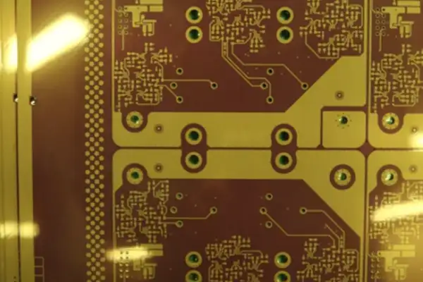
I have encountered far too many engineers who treat the Printed Circuit Board (PCB) as nothing more than a simple platform for electrical interconnections. In the field of power electronics, however, discovering thermal issues only after the board has been powered up is often a case of “too little, too late.” I once took over a project where, upon seeing the design board densely packed with power transistors, I immediately sensed that trouble was brewing. Sure enough, when the prototypes returned and underwent testing, the temperatures of several critical chips skyrocketed to a staggering 120°C. Such scenarios frequently carry the risk of “thermal runaway”—a dangerous positive feedback loop wherein, for instance, the semiconductor junction temperature exceeding its rated limit causes a decline in carrier mobility, which in turn exacerbates heat generation.
Many people harbor the naive belief that simply slapping on a heatsink will magically resolve all thermal issues. The true challenge lies in the fact that heat is conducted outward from the chip’s interior incrementally; every intervening layer of material introduces additional thermal resistance. Consider this: even if you employ the highest-quality thermal grease, the interface itself—the physical boundary between components—remains an inherent thermal bottleneck. In reality, the thermal resistance from the chip die to the case (θJC) alone often accounts for more than 30% of the total thermal resistance—to say nothing of the contact thermal resistance between the packaging material and the PCB (θCS), which is further susceptible to variations in surface flatness. When designing, I now prioritize considering the heat flow path of the entire system. For instance, in a recent project involving a vehicle-mounted inverter, I positioned the power components directly on the back edge of the PCB; by leaving a large, exposed copper area, I was able to mount them directly onto a liquid cooling plate. This allows heat to be conducted away in an almost linear path—a method far more effective than simply attaching heat sinks later in the process. Such a design necessitates early collaboration with structural engineers to verify the flatness of the mounting surface; simultaneously, one must calculate the Reynolds number for the coolant flowing through the cold plate channels to ensure efficient heat transfer via turbulence.
In fact, the PCB itself can serve as an integral part of the thermal management system; sometimes, simply adding a few thermal vias or adjusting the copper thickness can significantly improve temperature distribution. During one test, we discovered that increasing the copper thickness on the inner layers from 1 ounce to 2 ounces resulted in a direct 8-degree drop in junction temperature. Such subtle adjustments are often far more effective than relying on external heat dissipation devices. However, it is worth noting that increasing copper thickness can compromise etching precision—particularly for fine-pitch circuitry—requiring a careful balance between current-carrying capacity and manufacturing accuracy.
What gives me the biggest headache are designs that blindly prioritize miniaturization, packing components together like sardines in a can with absolutely no room left for airflow. As power density increases, the available surface area for heat dissipation actually shrinks—isn’t that a fundamental contradiction? Effective thermal management requires creating clear escape routes for heat, rather than simply confining all heat sources within a single enclosure. For example, in forced-air cooling systems, if the spacing between components falls below 3mm, “airflow shadow zones” can form, leading to localized heat accumulation.
I typically categorize thermal management strategies into several distinct tiers: the most fundamental approach involves leveraging the PCB’s inherent structural properties; the next level incorporates the use of auxiliary heat sinks; and the highest tier may require the consideration of active cooling solutions. For each specific project, the appropriate thermal management strategy must be selected based on actual power dissipation requirements; a one-size-fits-all approach is simply not feasible. For instance, consumer electronics might rely solely on natural convection, whereas industrial equipment may necessitate the adoption of heat pipe or vapor chamber technologies.
I recently experimented with embedding a metal substrate within a multilayer PCB stackup, and the results were surprisingly effective—particularly in scenarios involving severe localized heating, where heat could be rapidly dissipated laterally. This three-dimensional approach to thermal management is far more sophisticated than simply increasing copper thickness; while it does entail higher costs, the investment is well worth it in applications where high reliability is paramount. Practical testing has demonstrated that a 3mm-thick aluminum substrate can boost the thermal spreading angle from 45° to nearly 80°, thereby significantly reducing the concentration of thermal hotspots.
Ultimately, thermal management does not exist in isolation; it is inextricably linked to both electrical performance and mechanical structure. Sometimes, routing patterns must be adjusted to facilitate heat dissipation; this necessity, however, perfectly illustrates the true artistry of system design—finding the optimal balance amidst a multitude of constraints. For instance, high-frequency signal lines demand strict impedance control, yet widening copper pours for thermal purposes can compromise the integrity of the reference plane; in such cases, employing embedded resistor technology or localized depth-controlled milling may serve as a viable compromise.
The most extreme example I have ever encountered involved an engineer attempting to build a kilowatt-class power supply using standard FR4 material—only to have the PCB substrate burn out before the active components did. Selecting the appropriate substrate material constitutes the first line of defense in thermal management; regrettably, many engineers fail to identify this critical issue until they have already reached the mass production stage. In reality, the glass transition temperature (Tg) of standard FR4 typically falls between 130°C and 140°C, whereas high-Tg materials or ceramic substrates are capable of withstanding continuous operating temperatures exceeding 200°C.
Whenever I review a design these days, I invariably ask one additional question: “How do you intend to channel the heat generated by this specific component?” This seemingly simple inquiry often serves to expose a host of potential risks; after all, in the realm of power electronics, neglecting thermal management is tantamount to planting a ticking time bomb. I strongly recommend establishing a comprehensive thermal checklist—one that encompasses thermal parameter verification during component selection, thermal simulation validation during the layout phase, and a closed-loop thermal imaging verification process during the prototyping stage.
It pains me every time I witness engineers scrambling to retrofit fans onto overheating PCBs. It is truly a pity; these issues could have been entirely avoided had a little extra thought been invested during the initial design phase. Why wait until a crisis is literally “on your doorstep” before taking action? Thermal design should be shifted to the forefront—integrated into the conceptual design phase—and established as a standard procedural step (much like signal integrity analysis), rather than being treated as a mere afterthought or remedial measure.
I have encountered far too many people who oversimplify the complexities of PCB thermal management. They seem to operate under the misguided assumption that once the board layout is complete, they can simply offload the entire thermal challenge onto heatsinks and cooling fans. In reality, the truly tricky problems often emerge only after you’ve slotted the board into its enclosure.
I recall a specific project where everything ran perfectly during lab testing; yet, the moment we deployed it at the client’s site, it began triggering thermal overload protection alarms repeatedly. After much troubleshooting, we finally discovered that the airflow inside the enclosure was being completely obstructed by cables and other expansion cards. The intended airflow path had been rendered entirely ineffective, causing the temperatures of critical components to soar nearly 20 degrees higher than anticipated.
This experience taught me a crucial lesson: when it comes to PCB thermal management for power electronics, you absolutely cannot focus solely on the board itself. You must view and analyze the entire system as a cohesive whole. Thermal solutions that appear perfectly adequate in an open-air environment may prove completely inadequate once confined within a closed space.
Consequently, whenever I design now, I make a point of considering the enclosure layout right from the outset. For instance, I try to position power components as close as possible to the air intake vents, ensuring they remain clear of the hot-air exhaust paths generated by other heat sources. Sometimes, for the sake of thermal efficiency, it even becomes necessary to reorient the entire PCB layout.
Simulation tools can certainly be helpful, but only if your models are sufficiently realistic. I’ve seen instances where designers simply applied idealized heat sink models, resulting in simulation data that deviated from actual measurements by as much as 30 or 40 degrees. Truly useful simulations require incorporating every minute detail within the enclosure—including seemingly insignificant elements like cables and mounting brackets.
My greatest fear is when mechanical design lags behind the electrical design process. Designers might not think about integrating heat sinks until the PCB layout has already been finalized; by that stage, there is often little to no room left for adjustments. Consequently, I now require my team to bring the mechanical engineers into the discussion the moment we begin drafting the initial schematics.
In truth, thermal issues are rarely technical conundrums; rather, they are typically collaboration failures. Circuit engineers tend to view thermal management as the mechanical team’s responsibility, while the mechanical team complains that the circuit layout failed to leave adequate space for cooling solutions. The key to breaking this impasse lies in having someone take a holistic view from the very beginning—someone who can coordinate and optimize the entire system’s thermal flow path.
Sometimes, the simplest solutions prove to be the most effective. For example, simply ensuring there is sufficient clearance for airflow around critical components, or selecting PCB substrate materials with superior thermal conductivity. These subtle improvements in the details often yield far better results than retrofitting expensive, complex cooling apparatuses later in the design cycle.
After years spent designing thermal solutions for electronic devices, I’ve come to feel that those visually impressive “thermal cloud maps” can sometimes be quite misleading. I recall a high-power supply project where our team spent two weeks running thermal simulations, only to find that the moment we powered up the prototype, the temperature readings at our critical test points immediately exceeded the allowable limits. The problem lies in the fact that we idealized the chassis design too much; during actual assembly, cables obstructed critical airflow paths—a scenario that is simply impossible to model accurately in simulations.
When performing PCB thermal management for power electronics, the most vexing issue is undoubtedly the handling of boundary conditions. You sit in front of a computer screen, configuring various idealized parameters, yet the real-world thermal environment invariably proves far more complex than imagined. We once conducted a test where the same circuit board, when oriented horizontally versus vertically, exhibited a temperature difference of seven or eight degrees—simply because gravity influenced the airflow patterns. These subtle nuances are particularly prone to being overlooked during the initial simulation phase.
Nowadays, whenever I see newcomers holding up a simulation report and claiming it is absolutely infallible, I can’t help but chuckle. Last year, we were validating a model for an automotive inverter; although we had configured the convection coefficients strictly according to standard operating conditions, actual vehicle testing revealed that the temperature distribution within the engine bay was completely different. We later realized that we needed to account for the radiant heat emitted by adjacent components—a critical factor that had been entirely omitted from the initial simulation.
Simplifying models certainly saves time, but the cost may be far higher than anticipated. My standard practice is to deliberately set aside time for physical validation immediately after completing the preliminary simulations. On a project last month, it was only by working backward from actual measured data that we discovered a discrepancy between a specific chip’s package thermal resistance and the value listed in its datasheet. Such deviations are extremely difficult to detect through software simulation alone.
The truly reliable approach is to treat simulation as an exploratory tool rather than a definitive answer book. I typically run several simulation sets using varying boundary conditions to gauge sensitivity and identify the areas most susceptible to failure. For instance, regions with high-density power component layouts or areas adjacent to connectors often require a larger thermal margin in their temperature predictions.
Recently, we have been experimenting with a new methodology: integrating thermal design and structural design at a much earlier stage of development. After all, thermal performance depends not only on the PCB itself but is also inextricably linked to the mechanical layout of the entire system. Sometimes, simply shifting the position of a mounting screw or adjusting the orientation of a connector can yield significant improvements in thermal dissipation.
Ultimately, thermal management is an iterative process of trial and error. Simulation is an invaluable tool, but it cannot provide you with every answer. I have now cultivated a habit: after every simulation run, I ask myself, “Where is this result most likely to be flawed? What real-world factors have I yet to account for?” Maintaining this healthy skepticism actually helps us avoid a great many pitfalls along the way. I have seen far too many engineers make the same mistake regarding PCB thermal management for power electronics: placing excessive faith in the figures listed on material data sheets. In particular, whenever I see someone sparing no expense to stack up materials solely in pursuit of a high thermal conductivity coefficient, I feel compelled to remind them: thermal design is not merely a mathematical exercise.
I recall a project team that insisted on using the most expensive thermal interface material available—one boasting a conductivity rating close to 10 W/m·K. Yet, when actual testing was conducted, their thermal dissipation performance proved inferior to that of the neighboring team, which had utilized ordinary materials. It was later discovered that the issue lay in their installation process: they had compressed the thermal pad too thinly, resulting in poor contact and a failure to achieve proper surface adhesion.
Many people tend to overlook a critical point: no matter how excellent a material may be, if the installation process is flawed, its effectiveness can be cut in half. We once tested thermal pads of varying thicknesses and discovered that a 0.5 mm pad made of a mid-range material outperformed a 1 mm pad made of a premium material; this was simply because the thinner pad was better able to fill microscopic air gaps under the same applied pressure.
Speaking of embedded copper blocks, I actually feel this technique has been somewhat mythologized. While it is true that copper’s thermal conductivity can reach 380 W/m·K, in practical applications, that impressive numerical value often remains a theoretical advantage. I have encountered cases where thermal expansion mismatches led to delamination along the edges of the copper block; after just a few thermal cycling tests, cracks would appear at the interface, resulting in a decline in thermal dissipation efficiency.
The truly effective approach is to strike a balance tailored to the specific application scenario. Areas containing high-power components that require rapid heat extraction may warrant localized reinforcement, but there is no need to apply expensive solutions across the entire board. Sometimes, simply adding a few thermal vias or optimizing the component layout proves far more effective than blindly stacking up expensive materials.
Interface thermal resistance is a factor that is frequently underestimated. Even if you employ top-tier materials, if the surface finish is rough or the mounting pressure is insufficient, heat will remain trapped at the contact interface, unable to flow through effectively. In our laboratory, we once measured the impact of varying surface roughness levels on thermal conductivity and found that the performance gap could exceed 30%.
The cardinal sin of thermal design is blindly following trends. Every project presents a unique combination of heat source distribution, spatial constraints, and budgetary limitations; simply copying someone else’s solution often results in compromised performance. I now prefer to begin by conducting simple thermal simulations to identify the true bottlenecks, and only then select materials specifically tailored to address those issues.
Ultimately, effective thermal design is a matter of systems engineering—not merely a contest between individual materials. It requires simultaneous consideration of both the structural design of the thermal pathways and the treatment of the interfaces. Sometimes, investing a significant sum to upgrade materials yields far less tangible benefit than simply optimizing the assembly process. Whenever I see engineers poring over calculations to determine heatsink dimensions, I find myself wondering if we aren’t oversimplifying the problem. Thermal management in power electronics is never a matter that can be solved merely by swapping in a better heatsink; it is, rather, a test of systemic thinking.
I recall a project where our team spent a great deal of time optimizing the fin spacing of a heatsink, only to encounter overheating issues during actual operation. We later discovered that, within the confines of a sealed enclosure, the actual airflow fell far short of our theoretical projections. That moment brought home a crucial realization: no matter how perfect the design of an individual component may be, if it is divorced from its real-world operating environment, the effort may well be entirely in vain.
My focus now lies more on how to prevent the generation of excessive heat right from the initial design stages—for instance, by selecting more efficient circuit topologies or by distributing the power load across multiple components. Sometimes, a seemingly minor architectural tweak can significantly alleviate the overall thermal burden, sparing us the frantic scramble to dissipate heat after it has already been generated.
The testing phase is another area where it is all too easy to stumble into pitfalls. The controlled, constant 20°C environment of a laboratory is a completely different beast from the high-temperature, 45°C scenarios in which equipment actually operates. I have witnessed countless cases where a device performs flawlessly under standard test conditions, only to suffer from a cascade of failures once deployed in real-world operating environments. Factors such as component aging and fan performance degradation—dynamic variables that evolve over time—are often the true Achilles’ heel.
Truly effective thermal management requires incorporating thermal path design considerations right from the very moment power chips are selected. During the PCB layout phase, sufficient space for thermal diffusion must be allocated; one cannot simply wait until the final stages to start piling heatsinks onto the board. Material selection is equally critical; sometimes, switching to a substrate with a higher thermal conductivity yields far more tangible results than merely increasing the surface area of the heatsink fins.
A recent case study I encountered serves as a perfect illustration of this point. By optimizing the driving mechanism for the switching components, we were able to directly reduce power loss by 15%—a reduction that, in turn, drastically lowered the thermal requirements placed upon the heatsink. This approach—tackling the problem at its very source—is far more intelligent than frantically attempting to bolster heat dissipation as an afterthought.
I believe that what is most essential in this line of work is the ability to step back and view the “big picture” rather than getting bogged down in isolated details. When you find yourself agonizing over a specific detail, take a step back and ask yourself: Does this heat source truly need to exist? Is there a more elegant solution available? After all, the most effective thermal management is the kind that ensures heat never becomes a problem in the first place.
I remember when I first started designing high-power electronics, I operated under the assumption that I couldn’t go wrong by simply placing the heat-generating components off to the side—after all, the heatsinks were sitting right there, ready to do their job. It wasn’t until I had fried a few circuit boards that I finally realized: things are definitely not that simple. Particularly now that we are utilizing components like GaN, while they are capable of withstanding higher temperatures, the task of managing that heat has actually become more challenging. I once placed a GaN module right along the edge of a PCB; the thermal imager subsequently revealed that the edge area became hot enough to fry an egg, whereas the center of the board remained significantly cooler. I eventually figured out the reason: the heat was trapped in the corner with nowhere to dissipate. It would have been far more effective to position the heat source in the center of the board, allowing the thermal energy to spread out evenly.
Nowadays, whenever I engage in PCB thermal management for power electronics, I pay meticulous attention to component placement. I used to assume that the temperature parameters listed in datasheets were sufficient; however, actual debugging revealed a vast discrepancy between theory and reality. For instance, in one project involving GaN devices—which boasted a nominal junction temperature rating of 200°C—simply placing them slightly too close to the board’s edge caused all the adjacent components to fail simultaneously. Upon redesigning the layout, I relocated the power devices to the central region of the board; although this made the routing slightly more complex, it resulted in an overall temperature reduction of over ten degrees.
The most vexing aspect of these high-performance components is the phenomenon of thermal coupling. The heat generated during their operation is not distributed uniformly; instead, it tends to concentrate in specific “hot spot” regions. During one test, I discovered that the temperature on the underside of a particular chip was more than twenty degrees lower than that on its upper surface—a direct consequence of heat accumulating in a specific location without finding a path for dissipation. In such scenarios, merely looking at the maximum junction temperature parameter is entirely meaningless; the critical factor is how effectively one can facilitate the flow of heat.
Whenever I see someone still blindly adhering to the dogma that “heat-generating components should be placed along the edges,” I feel compelled to offer a word of caution. Every PCB possesses a unique thermal dissipation path. In certain designs, positioning components at the board’s edge indeed allows them to leverage the chassis for heat dissipation; however, when dealing with multi-layer boards or enclosed environments, this approach can actually create thermal traps. The key lies in understanding the fundamental principles of heat flow, rather than mindlessly memorizing so-called “best practices.”
A project I have been working on recently serves as a fascinating case study. Initially, following conventional wisdom, I distributed the high-power components across the periphery of the board; however, thermal imaging revealed that the board appeared to be encircled by a ring of fire. I subsequently decided to take the exact opposite approach: I consolidated all the major heat-generating components into the central region, leaving ample clearance around them for heat dissipation. The results were surprisingly effective. Sometimes, breaking away from conventional thinking is precisely what leads to the discovery of more rational and effective solutions.
Ultimately, thermal management is a discipline that demands a case-by-case analysis; there is no one-size-fits-all solution. Rather than blindly adhering to various design guidelines, it is far more productive to spend more time observing actual heat distribution patterns. After all, theory is gray, but the tree of life—and practice—is ever green.
I have seen far too many teams stumble on power electronics projects. They invariably treat PCB thermal management as a late-stage afterthought—acting as if simply finishing the board layout and slapping on a heatsink will magically solve all their problems. This mindset is, in fact, quite dangerous.
Truly savvy engineers begin contemplating thermal issues right from the architectural stage. For instance, when selecting a circuit topology, they consider which option will facilitate a more uniform distribution of heat. Sometimes, a simple shift in perspective—such as splitting a single heat-generating component into two separate parts—can significantly lower the overall system temperature. This approach is far more effective than agonizing over heatsink dimensions during the later stages of development.
I recall a particularly interesting project. Initially, the team was fixated on optimizing the thermal resistance parameters of their conductive materials. However, a senior engineer eventually proposed a complete redesign of the airflow paths within the chassis. The result? Not only did they save on expensive thermal pads, but the overall system temperature also came in ten degrees lower than projected. This difference in conceptual depth—this higher-level thinking—often determines the ultimate ceiling for a product’s reliability.
Nowadays, an increasing number of designs incorporate temperature monitoring capabilities. This is certainly a step in the right direction, but relying solely on sensors is not enough. The key lies in integrating thermal management into the entire development workflow—from schematic capture to PCB layout, and from component package selection to system-level integration. At every stage, engineers from various disciplines must collaborate to assess the thermal implications of their decisions. Mechanical design and real-world operating conditions are often overlooked by hardware teams; yet, these very factors are what ultimately determine a product’s performance in its actual operating environment. The data measured in a controlled laboratory setting can differ vastly from the actual performance observed at a customer’s site.
I recently encountered a case that serves as a perfect illustration of this point: a particular team’s thermal simulations appeared flawless during the design phase; however, once mass production began, they discovered that a specific capacitor was consistently failing prematurely. It was subsequently revealed that the mounting bracket had altered the local airflow patterns, causing the temperature at a specific “hot spot” to rise 20 degrees higher than anticipated. This type of issue cannot be detected by a PCB engineer working in isolation. Ultimately, thermal management is not the exclusive domain of any single department; it demands a system-level perspective. The more complex a power supply product becomes, the greater the need for a collaborative approach that breaks down departmental silos.
While recently debugging a power board, I realized that many people harbor misconceptions regarding PCB thermal dissipation. People often assume that simply adding a few thermal vias or stacking thicker copper layers will solve the problem; in reality, thermal design demands much more meticulous consideration.
I recall a specific testing session where, despite utilizing 2oz copper plating, a particular MOSFET still became excessively hot. We later discovered the root cause lay within the dielectric layer—heat was trapped beneath the surface and unable to dissipate downward. In such a scenario, even the thickest copper plating becomes akin to wrapping a thermos flask in a blanket: the surface temperature drops, but the internal heat remains trapped and cannot escape.
Speaking of thermal via placement, I once learned a lesson the hard way. In an effort to maximize heat dissipation, I once placed the vias extremely close together; surprisingly, the board developed micro-cracks during temperature cycling tests. Even more unexpected was the discovery that these densely packed vias effectively fragmented the copper plating, thereby weakening the board’s lateral thermal conductivity. Nowadays, I employ a differentiated layout strategy—placing vias differently in the corners versus the center of the chip area—to ensure both mechanical integrity and the continuity of the thermal diffusion pathways.
Thermal management for power devices cannot be viewed in isolation. On one occasion, a client complained that a specific IC kept triggering its thermal overload protection. Upon inspection, we discovered that an adjacent voltage regulator chip was effectively “baking” the entire surrounding copper pour area. Consequently, when redesigning the layout, we deliberately distributed the heat-generating components across the board, allowing each section of copper plating to fully contribute to the overall heat dissipation effort.
In truth, the most effective thermal solutions are often hidden within the simplest details. For instance, we once found that removing the solder mask from specific areas significantly improved heat dissipation, as the exposed copper surface allowed for direct convective heat transfer with the surrounding air. On another occasion, while working with an aluminum-substrate PCB, we experimented with dielectric layers of varying thicknesses; although a thinner dielectric layer (down to 100μm) offered slightly reduced electrical insulation, its immediate and dramatic improvement in thermal conductivity was undeniable.
These experiences have led me to view PCB thermal management for power electronics less as a static design task and more as an exercise in “thermal path planning.” You must clearly understand the heat’s origin, its intended destination, and any obstacles it might encounter along the way. Sometimes, simply adding a small thermal pad proves far more effective than merely increasing the copper thickness; the key lies in identifying—and addressing—the weakest link within the entire thermal dissipation chain.
I have long felt that, in the realm of electronic design, thermal management is—ironically—the issue most frequently overlooked. Many people focus their attention on circuit performance while overlooking the fact that temperature is the true determinant of a product’s lifespan.
I recall an instance where our team was designing a power supply module; the issue of PCB thermal management—specifically for power electronics—proved to be a major headache. In the lab, individual components tested perfectly; however, once installed in the complete system, the device would trigger its overheat protection after running for just half an hour. We eventually discovered that the problem stemmed from several heat sources being positioned too close together, creating a thermal coupling effect. This coupling is not a simple case of “one plus one equals two”; rather, the heat sources mutually exacerbate one another, causing local temperatures to skyrocket far beyond expectations.
Test environments often create a false sense of security. On an open workbench with excellent airflow, the measured data may look impressive; however, in actual use—when the device is enclosed within a sealed chassis and surrounded by other heat-generating components—the situation is entirely different. The temperature differential can reach 20 to 30 degrees Celsius—a margin sufficient to render an otherwise stable circuit unreliable.
I have witnessed countless cases where a failure to prioritize thermal management resulted in persistently high product return rates. Sometimes, the issue lies not with the design itself, but rather with a failure to account for the heat accumulation effects inherent in real-world operating scenarios. High temperatures not only shorten component lifespans but also alter circuit characteristics, creating a vicious cycle: rising temperatures lead to diminished efficiency, which in turn generates even more heat.
Nowadays, when designing, I pay particular attention to thermal planning during the layout phase—distributing high-heat components strategically and ensuring ample space for heat dissipation. Furthermore, I simulate the thermal field distribution of the entire system in operation, rather than merely testing individual modules in isolation. After all, electronic products are ultimately intended to function in real-world environments, not to remain perpetually on a laboratory workbench.
A truly reliable design must be capable of withstanding the rigors of actual operating conditions; this requires us to integrate thermal management considerations into every stage of the process—from initial concept through to final implementation.
A relay control board that works perfectly in the lab can fail
A medical pump PCB that performs flawlessly in the lab can produce
The ADAS controller PCB is no longer a passive substrate — it
- Expert på produktion av små till medelstora serier
- Kretskortstillverkning med hög precision och automatiserad montering
- Pålitlig partner för OEM/ODM-projekt inom elektronik
Öppettider: (mån-lör) från 9:00 till 18:30