
How to Choose a Reliable BLDC Motor Controller PCB Manufacturer for High Power Applications?
In the BLDC motor controller project, we are often attracted by the
I have seen far too many novice designers treat those small copper circles as nothing more than dispensable decorations. It is only when they witness—with their own eyes—an SMT machine misplacing a BGA chip that they finally realize the truth: those inconspicuous fiducials are, in fact, the “eyes” of the entire SMT assembly line.
I recall an instance where I was helping a friend revise a board design and stumbled upon an interesting phenomenon: the fiducials he had placed were positioned too close to the board’s edge, causing the machine’s vision system to consistently fail to focus. We subsequently resolved the issue by rearranging three of the fiducials into an irregular triangle configuration. This incident made me realize that while many people assume they can simply scatter a few markers haphazardly, every single detail in this process requires careful consideration.
Nowadays, many engineers rely excessively on automated routing software, inadvertently neglecting these fundamental design principles. During a recent factory tour, I encountered a textbook example of what not to do: the fiducials on a particular board shared the exact same surface finish as the component pads. Consequently, the machine vision system mistook the solder pads for positioning markers, resulting in an entire batch of components being placed askew.
The truly reliable approach is to maintain a sufficient clearance distance between these fiducials and the surrounding components, while also avoiding areas prone to glare or reflection. I make it a habit—when panelizing boards—to assign independent fiducials to each individual circuit unit. Although this adds a few extra minutes to the drafting process, it effectively eliminates the risk of an entire panel being scrapped on the assembly line.
Recent testing has revealed that fiducials treated with an Electroless Nickel Immersion Gold (ENIG) finish exhibit a significantly higher recognition rate in low-light environments compared to those with a Hot Air Solder Leveling (HASL) finish—a subtle detail that is often overlooked by the majority. Ultimately, a truly robust design is built upon a steadfast commitment to getting these minute details right.
What I find most striking—and somewhat baffling—is that there are still people today who believe these fiducials are intended for human visual inspection. I remember an intern once asked me if we could replace the copper pads with simple characters to save money; I nearly spat my coffee all over my screen. Modern production lines are entirely automated; those tiny dots serve as the medium for the dialogue between the machinery and the circuit board.
Ultimately, implementing these fiducial marks properly isn’t just about passing inspections; it represents a fundamental respect for the production line itself. After all, who wants to see the boards they’ve painstakingly designed end up as nothing more than a pile of scrap metal on the assembly line?
When designing circuit boards, I tend to view these fiducial marks as the “eyes” of the entire layout. Many people might dismiss these tiny markers as mere technical minutiae of the manufacturing stage, but I’ve found that they actually have a profound impact on the overall smoothness and efficiency of the entire production process.
I recall an instance where a board I designed nearly failed to be recognized by the pick-and-place machine because the fiducial marks were positioned too close to the board’s edge. Since then, I’ve made it a priority to ensure there is ample clearance around these markers, guaranteeing that the machinery can accurately capture their positional data.
Regarding the dimensions of the fiducial marks, I don’t believe in rigidly adhering to a single fixed value; the key is to consider the specific recognition capabilities of the actual production equipment being used. Sometimes, making them slightly larger—say, around 1 millimeter in diameter—can actually result in more stable and reliable detection. Of course, this ultimately depends on the precision specifications of the specific factory’s machinery.
The treatment of the solder mask layer is equally critical: you must ensure that the area surrounding the fiducial mark remains completely exposed, free from any covering. Any obstruction would compromise the contrast required by the machine’s vision system, rendering the marks ineffective and defeating their very purpose.
I personally prefer placing fiducial marks at the diagonal corners of the board; this ensures that the machinery can quickly establish a reference point regardless of how the board is oriented or rotated. I once experimented with adding a few auxiliary fiducial marks around particularly complex circuit modules; the result was a noticeable boost in production efficiency and a significant improvement in component placement accuracy.
In truth, every designer likely has their own preferences—some favor standard circular marks, while others find specific geometric shapes more practical. Ultimately, however, what matters most is the tangible result: does the design help minimize complications on the production line and ensure a smoother, more streamlined manufacturing process?
When all is said and done, these seemingly insignificant details often prove to be the deciding factors in the overall quality and stability of a product. They are well worth the extra time and effort required to get them right.
Whenever I look at a circuit board schematic designed by a novice and see those fiducial marks scattered haphazardly across the layout, I can’t help but sigh. These markers may appear inconspicuous, but they directly impact the efficiency and quality of the entire manufacturing workflow—and that, right there, is precisely where the problem lies! I recall an incident last year while helping a friend debug a PCB: we discovered that his fiducial markers were completely obscured by the machine’s clamping fixtures. This caused the entire component placement coordinate system to go haywire, necessitating a complete rework. That experience drove home a profound realization: the layout of fiducial markers is by no means a trivial task that can be satisfied merely by casually dropping a couple of circles onto the board.
In fact, many people tend to overlook a crucial point: the fundamental purpose of fiducial markers is to provide a stable reference for machine vision systems—they do not exist merely to “pad the numbers” through mindless, repetitive placement. Such mechanical repetition often stems from a disregard for detail. For instance, some engineers assume that simply placing two symmetrical markers in the corners of the board is sufficient. However, in actual production scenarios—such as when the board undergoes thermal deformation or the equipment experiences vibration—a two-point system is utterly incapable of correcting for nonlinear distortion errors. This is precisely where the value of a third fiducial marker becomes apparent; it enables the machine to calculate a more complex compensation matrix, effectively equipping the pick-and-place machine with a smarter pair of “eyes.”
I make it a habit to integrate the positioning of fiducial markers into the overall layout considerations right from the initial design phase, rather than attempting to patch up omissions as an afterthought. Such last-minute, reactive approaches often create more problems than they solve. For example, in a recent project I encountered, an engineer crammed the fiducial markers into a narrow strip along the board’s edge; consequently, when the board hit the production line, the conveyor belt’s guide rails ended up completely obscuring the recognition areas. Such seemingly trivial oversights in the details can, in reality, cause the yield rate for an entire production batch to plummet significantly.
Regarding the optimal number of markers, my experience suggests that for simple boards, two markers are indeed sufficient. However, when dealing with multi-pin ICs or high-density component layouts, three markers constitute a far more prudent and reliable choice. This is particularly true for larger PCBs, where a dispersed arrangement of fiducial markers can effectively mitigate the adverse effects of localized board deformation. In some instances, I even go so far as to place additional auxiliary markers around critical components; while this practice may appear redundant on the surface, it actually serves to enhance overall component placement precision.
Another point worthy of attention is the issue of symmetry. Some designers, in pursuit of aesthetic appeal, arrange their fiducial markers in a perfectly symmetrical pattern—only to forget that the machine vision system may need to distinguish the board’s specific orientation. If the board design allows for “reversible insertion” (i.e., it can be loaded into the machine in either a standard or inverted orientation), a symmetrical marker layout can easily lead to misidentification errors. Consequently, I now tend to favor arranging these markers in an L-shape or an irregular trapezoidal configuration; although such layouts may appear less symmetrical to the human eye, they deliver far more reliable results in practical application.
Ultimately, every minute detail within the PCB design process warrants serious attention. Seemingly simple elements like fiducial markers actually serve as a vital bridge connecting the design phase with the manufacturing phase. After all, doesn’t it stand to reason that any subsequent process optimization can only be truly meaningful if the foundational elements—such as these markers—have been established on a solid footing? Over my years of working with PCBs, I’ve come to realize something: those inconspicuous fiducials on a circuit board are actually far more critical than we often imagine. When I first started out, I, too, thought, “Aren’t they just a few tiny dots?” That mindset persisted until a mass production run went awry—I discovered that an entire batch of boards had been populated with misaligned components, and only then did the true significance of the issue hit me.
I recall an instance where I helped a friend troubleshoot their production line; their pick-and-place machine kept misplacing chips by about 0.3 millimeters. After hours of investigation, we finally discovered the culprit: one of the fiducials on the board was largely obscured by the solder mask. This caused a deviation in the machine’s vision system during recognition. That experience taught me a valuable lesson: failing to properly handle even a single minute detail can compromise the entire production workflow.
Nowadays, I often feel a sense of regret when I see novice designers simply placing fiducials in the corners along the board’s edges. In reality—especially with larger boards or those featuring high component density—it is essential to strategically place several auxiliary fiducials within the central regions as well. This practice effectively mitigates cumulative errors caused by board material expansion, contraction, or manufacturing tolerances.
Recently, while designing a high-density PCB, I conducted a specific experiment: I placed fiducials of different shapes in both the four corners and the central area of the board. The results were striking—the component placement accuracy in the central region improved by nearly 20% compared to traditional layouts. This discovery has prompted me to re-evaluate certain conventional practices and established norms within traditional PCB design guidelines.
In truth, the function of fiducials extends far beyond merely assisting the pick-and-place machine with positioning. From aligning the solder stencil to facilitating subsequent Automated Optical Inspection (AOI), every stage of the process relies on these tiny markers to ensure consistent precision. At times, I even view them as the coordinate origins of the circuit board itself; without them, the entire production workflow would lose its fundamental reference baseline.
It has become my standard practice to treat these fiducials as functional components during the design phase—rather than simply tacking on a few random dots as an afterthought at the very end. After all, when a board is populated with hundreds of components, even a microscopic error—measured in mere microns—can be amplified into a critical, system-level failure.
I have long felt that the most easily overlooked elements in PCB design are these tiny reference markers. I vividly recall a time when I nearly stumbled over this very issue while designing a high-density circuit board. In an effort to conserve space, I had positioned the pads for several components too closely together without leaving adequate visual markers for identification. Consequently, the pick-and-place machine misaligned the chips, necessitating a complete rework of the entire batch of boards. That costly lesson indelibly impressed upon me the paramount importance of precise positioning. Many people might assume that simply laying out the components clearly is sufficient; however, the variables involved in the manufacturing process are far more numerous than you might imagine. For instance, there is the slight deformation of the PCB substrate when subjected to heat, or the minute positional shifts that occur when separating a panelized board into individual units. These subtle details cannot be compensated for merely by relying on the dimensions specified in the design drawings; instead, they require machine vision systems to perform real-time corrections. Since vision systems require distinct reference points to function effectively, specialized fiducial markers—specifically designed for recognition—must be placed in the vicinity of every component requiring precise positioning.
I make it a practice to place two such markers diagonally across from critical chips—particularly for devices with fine lead pitches, such as those in BGA or QFP packages. Missing even a single marker can cause the pick-and-place machine to misjudge the component’s orientation. I once compared two design strategies: one utilized only global fiducials placed along the board’s edges, while the other incorporated local fiducials next to every major chip. The latter approach yielded a significantly higher first-pass yield rate. Although it took a few extra minutes to incorporate these markers into the design, it saved a great deal of trouble during the subsequent debugging and production phases.
Regarding the handling of panelized boards, many designers tend to overlook the importance of overall alignment. When multiple small boards are combined into a single large panel for mass production, focusing solely on the alignment of individual boards can lead to overall positional offsets, resulting in misregistration during the solder paste stenciling process. My standard practice is to place dedicated panel fiducials on the process borders (tooling strips) of the panel. This allows the equipment to first lock onto the entire large panel before refining the alignment down to the individual board level—a hierarchical positioning strategy that delivers much more stable and reliable results.
In fact, the design of these markers itself requires careful consideration; overly complex shapes can actually interfere with the recognition process. I typically opt for simple circular shapes with a matte surface finish to prevent glare from compromising recognition accuracy. Additionally, I ensure these markers are placed away from areas with dense routing, leaving sufficient clear space around them. After all, the fundamental purpose of these markers is to be read by machines; therefore, clarity and machine readability take precedence over aesthetic appeal.
Ultimately, these seemingly auxiliary design elements often determine the success or failure of the manufacturing process. Nowadays, whenever I review a PCB design, I make a point of specifically checking the placement of the fiducial markers; it has become an ingrained professional habit.
I have encountered countless novice designers who overlook a seemingly insignificant—yet absolutely critical—detail when designing PCBs: those small, circular fiducial markers. Many assume these copper dots are merely reference points intended solely for machine vision systems; however, anyone who has experienced the realities of manufacturing knows that they serve as the precise anchor points for the entire assembly workflow.
I recall an instance where I was helping a friend review the mainboard design for a smartwatch. I discovered that, in an effort to save a mere few millimeters of board real estate, he had completely omitted the local fiducial markers for several critical components. When the sample boards finally arrived, the 0402-package capacitors and resistors were placed haphazardly—some were even crooked—and several pins on the BGA chips had failed to align with their corresponding pads. We subsequently added a sufficient number of fiducial markers at critical locations, enabling the pick-and-place machine to accurately calculate the placement offset for each specific zone. As a result, our yield rate skyrocketed directly from 60% to over 95%.
Nowadays, whenever I work on high-density PCBs, I pay particular attention to ensuring that an adequate number of fiducial markers are strategically distributed across various regions of the board. This is especially crucial for larger boards or those requiring multiple reflow soldering passes; without fiducials, the dimensional distortions caused by thermal expansion and contraction can wreak havoc on the placement accuracy. I recall a specific instance involving an automotive electronics board: because we had placed global fiducials only along the board’s edges, the QFN chips located in the central region exhibited significant placement errors after passing through the reflow oven for the second time.
In essence, these markers serve as “eyes” for our automated assembly equipment. When a PCB enters the pick-and-place machine, its cameras rapidly capture the actual physical locations of these markers; by comparing these captured positions against the original design coordinates, the machine can automatically correct the component placement coordinates. While this process may appear simple on the surface, for boards demanding high precision, even a minuscule offset of just 0.1 millimeters can be enough to render an entire production batch unusable.
I recently encountered a rather interesting case involving a medical device client who insisted on using a unique cross-shaped marker as the fiducial reference for their panelized PCB design. However, during production, we discovered that this non-standard shape lacked the recognition stability of traditional circular markers. Consequently, the system required multiple recalibration attempts every time it calculated the panel’s placement offset, which—ironically—ended up reducing our overall production efficiency.
As a result, I’ve established a strict protocol for my team: any BGA or QFN chip with a pitch (pin spacing) of less than 0.5mm must be accompanied by localized fiducial markers; furthermore, global fiducials must be positioned along the board’s diagonals. For panelized designs, we now strictly utilize standard circular markers, ensuring that each individual sub-board within the panel possesses its own independent set of calibration references. These hard-won lessons were learned at a significant financial cost—paid for in “real gold and silver.”
Ultimately, effective PCB design entails more than just optimizing electrical performance; it also requires laying a solid foundation to facilitate the manufacturing process. Those meticulously positioned fiducial markers—seemingly insignificant details—quietly serve as the guardians of precision throughout the entire production workflow. After all, even the most flawless circuit design counts for absolutely nothing if the components cannot be placed in their correct, precise locations. Sometimes, watching a pick-and-place machine rapidly identify fiducial markers, it feels as though it is performing a precise GPS-guided navigation for the circuit board. The placement point of every single component is fine-tuned and corrected by this intelligent system; the resulting industrial aesthetic—a blend of precision and coordination—is truly awe-inspiring.
I have always felt that the most easily overlooked aspect of PCB design is those tiny little markers. Many people focus their entire attention on routing and component layout, failing to realize that these inconspicuous fiducial markers are actually the critical factor determining assembly quality. I recall an instance where our team was rushing to design a board; in an effort to save time, we haphazardly placed just a few markers. Consequently, the pick-and-place machine encountered recognition errors during assembly, causing the soldering positions for the entire batch of components to be misaligned.
In reality, the function of these markers is far more significant than one might imagine. For instance, when handling high-precision components such as BGAs, if the adjacent fiducials are not sufficiently clear, the machine struggles to achieve accurate positioning. I have witnessed numerous cases where, despite a flawless circuit design, the final product yield was severely compromised simply because these minute details were not properly addressed.
Nowadays, whenever I undertake a design project, I pay particular attention to the placement of fiducial markers. It is not enough to merely place global positioning points at the corners of the board; one must also configure specific local reference markers around each high-precision component. This is especially critical when the board features a mix of components varying significantly in size, necessitating a multi-tiered positioning strategy. Sometimes, I even add auxiliary markers diagonally across from specific critical components to enable the pick-and-place machine to capture the exact position of each component with even greater precision.
A recent project served as a profound lesson in this regard. The board in question featured a chip with a fine pitch of 0.4mm. Initially, we had placed only the standard global markers along the board’s edges; however, during the trial production run, we discovered that the placement of this specific chip consistently exhibited a slight deviation. We subsequently added two dedicated fiducial markers in the immediate vicinity of the chip, and the problem was instantly resolved. This experience reinforced my understanding that different types of components require varying levels of positioning support.
A well-designed set of fiducial markers should function like a detailed map provided to the machine. It must not only indicate the overall orientation of the board but also establish clear landmarks for every critical location. After all, even the most advanced equipment requires clear reference points to perform at its absolute best. This is precisely why I now treat the design of fiducial markers as an indispensable element—and one that demands serious attention—within the entire PCB layout process.
Sometimes, watching a pick-and-place machine rapidly and precisely complete its assembly tasks, I am reminded of the ingenuity hidden behind those seemingly simple fiducial marks. They act as silent guides, ensuring that every component lands exactly where it belongs. This exquisite interplay is precisely what makes modern electronics manufacturing so fascinating.
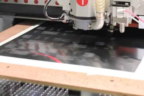
I’ve always found those small dots on PCBs particularly intriguing. When I first started out in circuit board design, I paid absolutely no attention to their existence—weren’t they just a few copper markings? It wasn’t until I witnessed a pick-and-place machine in action on a production line that I had my “aha!” moment.
The scene unfolded during a visit to an SMT assembly plant in Shenzhen: a robotic arm hovered mid-air, repeatedly adjusting its position but refusing to descend. An engineer pointed to a corner of the board, explaining that the problem lay right there—it turned out the reflective coating on one of the fiducial marks had been scratched. Because of this single, seemingly insignificant detail, the entire production line ground to a halt for half an hour.
Later, I encountered a similar situation with boards I had designed myself. In one particular batch, the dimensions of the PCB fiducials were slightly undersized, resulting in a minor misalignment during the solder paste printing process. Although the deviation was merely a few tenths of a millimeter, it was enough to cause the tiny 0402-package resistors to “stand up and dance” during reflow soldering.
In reality, many people tend to overlook the critical relationship between fiducial marks and component placement. For instance, failing to place local fiducials around a BGA package is akin to walking a tightrope blindfolded; the pick-and-place machine is forced to rely solely on extrapolation to pinpoint the exact locations of those invisible solder balls.
Solder paste thickness can also be a “silent killer.” During one round of testing, we discovered that using the exact same stencil parameters yielded vastly different results across different batches of boards. We eventually traced the issue back to fluctuations in the thickness of the solder mask layer surrounding the fiducial marks, which compromised the precision of the laser-guided positioning system.
Nowadays, whenever I review a new design, I pay special attention to three specific areas: the global fiducials located at the corners of the board; the auxiliary fiducials positioned around high-density component clusters; and the compensation fiducials situated at both ends of elongated modules. These seemingly simple geometric copper shapes often hold the key to the entire board’s ultimate success—or failure.
Recently, I helped a friend revise the design for a smart home module. He initially assumed that simply adding a few extra test points would boost his yield rate; however, we discovered that the true culprit—and the element requiring adjustment—was the spatial relationship between the fiducial marks and the ground plane. Once we made those specific tweaks, the component placement accuracy immediately jumped by 18%.
Ultimately, these fiducial marks serve as signposts for the machines; the clearer and more precise you make them, the more obediently and reliably your production line will perform. Sometimes, it is the most fundamental design details that best reveal an engineer’s true expertise; after all, even the most complex circuits must ultimately translate into the tangible reality of the manufacturing process.
Those small dots on a PCB are actually quite fascinating. When I first started working with circuit board design, I didn’t pay much attention to the purpose of these markings. Later, however, I discovered that these seemingly inconspicuous fiducial marks play a critical role during the surface-mount assembly process.
I recall an instance where our factory encountered an issue while manufacturing a batch of high-density circuit boards. The pick-and-place machines kept failing to align correctly, resulting in a drop in yield. Upon investigation, we discovered that the design of the PCB fiducials did not adhere to proper standards. The surface finish applied to these fiducial marks directly impacted the accuracy of the machine’s optical recognition system.
I have found that the ideal approach is to leave the fiducial marks as exposed copper. This ensures both sufficient optical contrast and the necessary surface flatness required for accurate recognition. Although some engineers prefer to apply a surface finish to the fiducials, an overly thick plating layer can actually compromise recognition precision.
Regarding the placement of fiducial marks, I have a small tip to share: it is best to place one at each of the board’s diagonal corners, as this helps the equipment establish an accurate coordinate system. Additionally, you must ensure that sufficient clearance is left around these marks to prevent other components from interfering with the visual recognition process.
On one occasion, while testing circuit boards made from various substrate materials, we observed an interesting phenomenon. Boards made from certain specialized materials would experience minute shifts in fiducial position due to thermal expansion and contraction. This served as a reminder that, during the design phase, we must account for the impact that the specific properties of the board material may have on overall precision.
Nowadays, whenever I undertake a design project, I pay particular attention to these minute details; after all, even the most advanced manufacturing equipment requires clear and accurate reference marks to perform at its absolute best.
Those inconspicuous little dots on a PCB are, in fact, quite intriguing. When I first began designing circuit boards, I simply viewed them as mere markings—nothing more. It was only later that I realized the precise placement of these fiducial marks directly influences the recognition efficiency of the pick-and-place machines. I once designed a board where the fiducial marks were positioned too close to the board’s edge, causing the pick-and-place machine to repeatedly generate error messages. It wasn’t until a technician from the production floor brought the board over to me that I fully grasped the root cause of the problem.
Consequently, whenever I design a board now, I make a point of ensuring that ample clearance is allocated for the fiducial marks. After all, the equipment on an SMT assembly line relies entirely on optical vision systems for positioning. If the fiducial marks are obstructed or exhibit inconsistent light reflectivity, it can disrupt the entire production rhythm of the assembly line. My standard practice is to place fiducial marks at three distinct corners of the board, thereby establishing a robust triangular positioning reference. This ensures placement accuracy even if the PCB undergoes slight deformation due to heat during the assembly process.
Different types of components impose varying requirements on fiducial marks. Precision packages—such as QFPs—demand particularly rigorous dimensional control. Consequently, I typically designate dedicated local fiducials for these components rather than relying solely on global marks. While this entails a slight increase in design effort, it significantly enhances placement quality.
A recent project provided me with a fresh perspective on fiducial marks. The client required high-density assembly on a flexible PCB. Standard circular fiducials proved susceptible to optical distortion when the board flexed; the issue was ultimately resolved by switching to cross-shaped fiducials. This experience taught me that design standards are not immutable; they must be flexibly adapted to suit the specific application scenario.
Effective design should simplify and ensure the reliability of the manufacturing process; those small dots tucked away in the corners of the board serve precisely as the bridge connecting design and manufacturing. Whenever I observe a pick-and-place machine precisely seating a chip onto its pads, I am reminded of these unsung positioning marks—for they are the critical details that ensure the entire workflow proceeds smoothly.
In the BLDC motor controller project, we are often attracted by the
From the production dilemmas of irregularly shaped boards to practical observations on
In the PCB manufacturing process, we once experienced a large number of
- Expert på produktion av små till medelstora serier
- Kretskortstillverkning med hög precision och automatiserad montering
- Pålitlig partner för OEM/ODM-projekt inom elektronik
Öppettider: (mån-lör) från 9:00 till 18:30