
Industrial Automation PCB Reliability: How to Achieve 10+ Years of Stable Operation
In the field of industrial automation, people often pay attention to AI
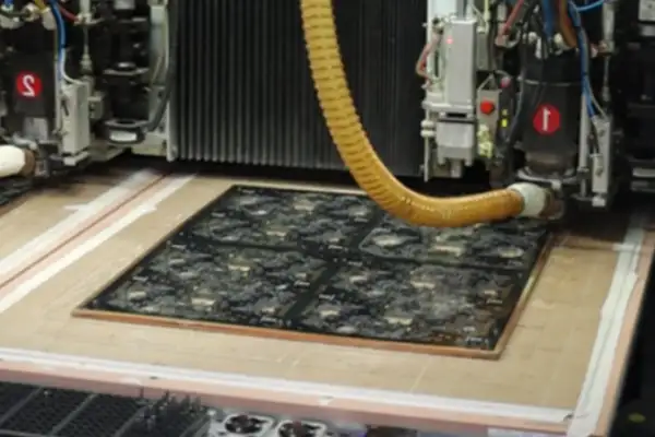
Every time I see those densely packed BGA packaged chips on a PCB, I find it quite interesting—this thing looks high-end, right? But behind it lies a lot of headaches. I’ve seen too many people blindly pursue high-density routing, resulting in no place for test points and ultimately making even basic circuit continuity testing impossible. Not to mention the solder joints hidden directly beneath the chip; problems there are like a game of hide-and-seek.
Some people believe X-ray machines can solve everything, but when actually repairing a board, you can’t rely on a machine to tell you the stress state of every solder joint, can you? I once encountered a board where the BGA solder balls looked perfect, but once powered on, the signal jumped erratically. After much troubleshooting, I discovered that residual stress from the PCB lamination process had slowly torn the solder joints apart. This kind of problem can’t be detected by conventional testing; it requires temperature cycling tests or even disassembly and analysis to pinpoint the issue.
Currently, many designs use laser micro-vias with diameters as small as pinpoints to save space for test points. It’s not that this technology is bad, but you have to consider the feasibility of subsequent repairs! Last time, a customer insisted we cram all the test points into the BGA area; during rework, even the probes couldn’t penetrate, and the entire board had to be scrapped.
I think it’s better to leave room for error in the design phase than to over-rely on testing methods, such as reserving a few redundant pads around the BGA for emergency rework. When selecting PCB materials, don’t just focus on perfect parameter matching; leaving some thermal expansion margin can actually extend solder joint life. I’ve seen too many cases where rigidly adhering to theoretical data backfired in practical applications.
Truly reliable quality control treats design, materials, processes, and testing as a closed loop. Just like cooking, good ingredients alone aren’t enough; the cooking time, seasonings, and even the plating method all need to be right.
I’ve always felt that many people have a misconception about BGA design—they think that minimizing the pitch is the entirety of technological breakthroughs. The real test of skill lies in maintaining reliability within a limited space. A project I worked on last week gave me a profound lesson: the client insisted on a 0.3mm pitch BGA PCB design, and in the sample stage, we discovered near-short circuits between the pads.
Some manufacturers are pushing solder mask bridges to their limits in pursuit of impressive parameters. I’ve seen people show off 0.08mm solder mask bridge widths with microscope photos, but in actual mass production, even slight temperature fluctuations can cause uneven ink coverage. Such designs might look good in a lab, but they simply cannot withstand real-world testing. For example, during reflow soldering, when the PCB experiences high-temperature shock, an excessively thin solder mask layer may shrink or crack due to thermal stress, leading to solder migration. Worse still, in humid or dusty industrial environments, tiny solder mask defects can gradually amplify, eventually causing leakage or short circuits between adjacent pads. This hidden danger may not manifest in initial functional testing but can suddenly erupt after several months of product use, causing large-scale field failures.
Regarding surface treatments, more and more people are questioning the value of the ENIG process. While its flatness is indeed suitable for high-density layouts, the black pad issue remains a constant concern. Last year, one of our medical device projects was switched to immersion silver treatment midway through due to this issue. Although the cost was higher, at least we didn’t have to worry about soldering failures all the time. While immersion silver treatment requires stricter packaging and storage control regarding initial oxidation sensitivity, its higher surface activity helps form a more robust intermetallic compound layer. Especially in scenarios requiring multiple reworks or long-term temperature cycling, the solder interface stability of immersion silver is often superior to ENIG, which is crucial for medical or automotive electronics requiring zero defects.
Sometimes I feel the industry is too obsessed with numbers. For example, they always emphasize linewidths in micrometers and stacking layers, ignoring a fundamental fact: even the most advanced technology ultimately comes down to the production line. I once visited a long-established PCB factory in China. Their equipment wasn’t the latest, but the experienced technicians could judge the state of the plating solution based on their experience. These details are the key to the quality of BGA pads. For instance, they would observe the fineness and color changes of the foam on the plating solution surface to predict minute fluctuations in copper ion concentration and adjust the current density accordingly. This experiential knowledge avoids “dog-bone” defects at the pad edges and ensures coplanarity of the solder balls—process details that automated equipment struggles to capture in real time.
Many young engineers now like to directly apply chip manufacturers’ design guidelines, which isn’t inherently wrong, but they need to understand that those parameters are often derived under ideal conditions. When actually making products, you have to consider factory humidity, equipment aging, and even differences in operator technique. It’s like playing a jigsaw puzzle; you can’t just stuff in the shiniest pieces—you have to ensure the whole picture fits perfectly. For example, the soldering profile recommended in the guidelines might be based on brand-new hot air reflow soldering equipment, but aging heaters in actual factories can cause deviations in the heating slope. In this case, compensation for the preheating and reflow zones needs to be made based on thermocouple measurements; otherwise, the solder balls in the BGA corners may not melt completely, forming cold solder joints.
Recently, while redesigning an industrial control motherboard, I intentionally increased the diameter of the BGA corner pads by 5%. This might seem to violate the principle of equal spacing, but it actually allows for thermal expansion. Some rules need to be respected, but some need to be broken; the key is to understand why. This adjustment is based on an in-depth analysis of the CTE differences between the PCB and the chip substrate: during temperature cycling, the package corners bear the greatest mechanical stress; moderately increasing the pad size increases the solder fill volume, absorbing stress through plastic deformation. Simultaneously, we adjusted the stencil opening scheme to ensure that corner solder joints are 10-15 micrometers thicker than the center area, further optimizing stress distribution.
I’ve always found making circuit boards quite interesting. Especially those boards with ball grid array (BGA) packages—what we commonly call BGA PCBs—always remind me of playing jigsaw puzzles as a child. Only now we’re assembling micron-sized components.
I remember once helping a friend repair an old graphics card. When I took it apart, it was covered in densely packed BGA-packaged chips made up of solder ball arrays. I thought to myself—how could such tiny things support an entire graphics processing system? Later, I gradually realized: the key isn’t how strong each individual solder joint is, but whether the entire array can distribute the stress evenly.
Many people think the most difficult part of making these high-density boards is the wiring. I think the real test of skill is how to distribute heat evenly across the entire substrate. I’ve seen too many cases of solder joints cracking due to localized overheating—especially in designs that integrate the processor and memory onto a single substrate.
Speaking of heat dissipation, we must mention the choice of substrate material. Some people are obsessed with expensive materials, but ordinary FR4 with a reasonable copper foil distribution can solve most problems. The key is to allow sufficient buffer space for thermal expansion, since the coefficients of thermal expansion of different materials vary significantly.
I once tested two different pad designs in the lab: a traditional circular pad and a slightly elliptical design. The latter performed better in temperature cycling tests. This made me realize that sometimes small shape adjustments are more effective than changing materials.
Now, seeing designs that pursue extreme density seems a bit misguided. Reaching pin pitch below 0.3mm is impressive, but is such an extreme approach really necessary in practical applications? At least 30% of the projects I’ve handled failed due to excessive miniaturization.
Recently, I was working on a flight control motherboard for a drone company. They initially insisted on cramming in five BGA chips, but after my suggestion, they reduced it to three plus peripheral circuitry, resulting in a 40% improvement in stability. This further convinced me that
ultimately, making circuit boards is similar to cooking—it’s not about adding more seasonings to make it tastier; the key is whether the various ingredients blend together perfectly. The simplest-looking designs are often the ones that stand the test of time.
I’ve always found PCB surface treatment a fascinating topic. A few days ago, a client brought me their newly designed BGA PCB and asked which process would be most suitable. Each treatment method has its unique characteristics.
Take OSP, for example. It’s indeed cheap and produces a smooth finish. However, I’ve seen too many examples of decreased solderability due to poorly controlled storage time, especially for multilayer boards requiring multiple reflow soldering cycles. Once, a small batch of samples we made was stored in the warehouse for over four months, resulting in widespread defects during soldering.
Immersion silver plating is quite suitable for cost-sensitive projects that require stability. However, you must ensure the production environment is free of sulfide contamination. I remember a factory where the entire batch of boards turned yellow because the workshop was near a chemical plant, ultimately forcing them to be scrapped.
Speaking of microvia technology, it’s becoming increasingly sophisticated. During my last visit to a supplier’s factory, I was truly impressed to see them achieving apertures below 50 micrometers. However, controlling the aspect ratio remains a challenge, especially as board thickness increases, leading to uneven copper plating at the bottom of the holes.
The through-hole design does save a lot of space, but it requires extremely high flatness. We once had a project where uneven filling caused cold solder joints after BGA soldering; we only solved the problem by switching to a partial through-hole process.
These experiences taught me that there is no perfect process, only the most suitable solution. The key is to choose based on the actual application scenario of the product.
I’ve always found BGA packaging quite interesting, especially the details of the soldering process that are invisible to the naked eye. Once, I disassembled a refurbished mobile phone motherboard and found several small voids hidden under the BGA solder balls. Although the equipment was still usable, these voids were like time bombs under long-term high temperatures.
Many people think that BGA soldering is just a matter of adjusting the machine parameters, but actually, plating quality is fundamental. I’ve seen many cases where inadequate surface treatment of the solder pads led to tiny gaps between the solder balls and the pads. These problems are difficult to detect under normal inspection, but the products will start to have problems after about six months of use.
One client who makes industrial control equipment left a deep impression on me. Their BGA PCBs consistently exhibited sporadic failures during aging tests. Microscopic examination revealed uneven plating thickness on the solder pads. Some areas were too thin, allowing solder to penetrate beneath the plating at high temperatures, creating a phenomenon known as “black pads.” This defect is more insidious than voids and has a greater impact on reliability.
Currently, some manufacturers simplify the plating process to save costs, resulting in poor solder ball adhesion. The difference in thermal expansion coefficients between the solder balls and pads during temperature changes leads to stress concentration. The most extreme case I’ve seen involved BGA devices in automotive electronic modules, where poor soldering quality caused mass failures in northern winters.
In reality, even the most advanced testing methods are no match for solid fundamental processes. X-rays can reveal obvious defects, but issues like the microstructure of the plating layer require cross-sectional analysis. Sometimes, I feel we rely too heavily on testing data, neglecting the most basic process control. Good BGA soldering should be a holistic reliability, not something guaranteed by a single step.
I’ve recently encountered some military-grade BGA packaging requirements, and their control over void ratios is incredibly stringent. This made me wonder if the consumer electronics industry is overly focused on cost optimization. After all, users won’t disassemble a phone to check the solder joint quality, but long-term stability will definitely be affected.
Ultimately, BGA reliability is a systemic issue. From PCB material selection to surface treatment, from soldering parameters to testing standards, every step must be taken seriously. Sometimes, simply and crudely copying standards can create hidden problems; the key is to grasp the quality requirements based on the specific application scenario.
I always find it quite interesting to see those densely packed BGA-packaged chips on a PCB. Many people immediately talk about various parameters or testing procedures, but I think the problems often lie at a more fundamental level. For example, sometimes we focus too much on complex testing methods while neglecting the simplest assembly environment.
I remember once spending a lot of time debugging a board, only to find that the humidity in the workshop wasn’t properly controlled, causing unexpected problems during soldering. These seemingly insignificant details can directly affect the soldering quality of BGAs. After all, each solder joint on a PCB is not isolated; they collectively form a complete connection system.
When it comes to BGA PCB design, I think you can’t just look at the size or spacing of individual pads. You have to consider the overall picture, including the matching of thermal expansion coefficients. Different PCB materials expand and contract differently when heated. If the expansion coefficients of the BGA chip and the substrate differ too much, even the most perfect soldering process won’t withstand repeated temperature changes.
Another easily overlooked point is PCB flatness. I’ve seen many cases where the soldering process itself is fine, but slight deformation of the board during manufacturing causes some areas of the BGA solder balls to not make contact with the pads. This kind of problem is difficult to completely solve with later X-ray or cross-section analysis; the quality of the substrate must be controlled in the early stages of manufacturing.
In fact, after working in this industry for a long time, you’ll find that many times the problem isn’t in the high-tech aspects, but rather in the most basic dimensions that haven’t been done properly. For example, cleanliness. If there are invisible contaminants on the PCB surface, even the most advanced reflow soldering equipment won’t guarantee a good soldering result.
I now tend to view BGA PCB design as a multi-dimensional engineering problem. From material selection and manufacturing processes to design specifications and the production environment, every step is interconnected. Simply pursuing a single technical indicator can easily lead to a loss of overall control.
Sometimes, the simplest solutions are the most effective. For example, strengthening incoming material inspection and optimizing workshop environmental control—doing solid foundational work is far more cost-effective than conducting a series of complex failure analyses later. After all, tracing the root cause after a problem occurs is much more expensive.
I believe a balance should be maintained in both the design and manufacturing stages. We cannot focus solely on technical parameters while ignoring the needs of the actual application scenario. Ultimately, every board will be installed in equipment and operate for extended periods; reliability is the final evaluation criterion.
In the field of industrial automation, people often pay attention to AI
Ever wonder how your phone maintains a stable signal? It relies on
When selecting components for a security monitoring system, most attention goes to
- Expert på produktion av små till medelstora serier
- Kretskortstillverkning med hög precision och automatiserad montering
- Pålitlig partner för OEM/ODM-projekt inom elektronik
Öppettider: (mån-lör) från 9:00 till 18:30