
Industrial Automation PCB Reliability: How to Achieve 10+ Years of Stable Operation
In the field of industrial automation, people often pay attention to AI
I’ve always found the field of flexible circuit boards particularly interesting. Many people may not understand how they are actually made. Take some flexible PCB manufacturers I’ve encountered, for example; their biggest headache is often not the design itself, but the performance of the materials during processing.
I remember once visiting a factory and seeing how they maintained a constant temperature and humidity throughout the entire production line when processing ultra-thin copper foil. The worker told me that even slight environmental fluctuations can cause tiny wrinkles in the copper foil during etching. These wrinkles can easily become fracture points during later bending tests. For example, in the etching tank, the corrosion rate of the etching solution on the copper foil varies with temperature, leading to localized stress concentration. These microscopic defects may only manifest as differences in gloss on a macroscopic scale, but they significantly affect the material’s fatigue life.
The most fascinating aspect of FPC is its adaptability. For instance, the circuit boards in wearable devices need to bend repeatedly with wrist movements. This isn’t simply a matter of placing the circuitry on a flexible substrate. Good manufacturers consider the circuitry’s routing during the etching stage, ensuring critical lines avoid areas of frequent bending. They typically use serpentine traces or grid-like copper plating designs to evenly distribute stress across the entire circuit area, preventing excessive localized stretching. They also use a more flexible polyimide substrate in the bending areas, with ductility that is more than 40% higher than ordinary materials.
Once, I received a failed sample and found tiny cracks in its overlay at the bending point. It was later discovered that the problem stemmed from improper temperature control during lamination, resulting in the adhesive layer not fully filling the gaps between the circuits. This issue might not be noticeable during static use, but it becomes apparent during dynamic bending. In fact, a proper lamination process requires a heating rate controlled at 3-5°C/minute and pressure holding at 120°C to ensure the adhesive fully flows and fills the micron-level gaps between the circuits.
A very intuitive way to judge the quality of a flexible PCB is to observe its resilience after bending. Some low-quality products will develop permanent creases after a few bends, while high-quality products can maintain their original shape even after tens of thousands of tests. This is due to the difference in material memory effect; high-quality FPCs use modified polyimide with a molecular chain design that provides better elastic recovery.
The most precise FPC circuits I’ve ever seen are only half the width of a human hair. This level of precision demands extremely high precision in the etching process, requiring meticulous control of the etching solution concentration and spray pressure, much like sculpting an artwork. Even a slight deviation will result in jagged edges on the circuits, affecting signal transmission. Modern high-end production lines employ closed-loop control systems, automatically adjusting nozzle oscillation frequency through real-time monitoring of the etching rate to control linewidth tolerance within ±3 micrometers.
Many electronic products now strive for lighter and thinner designs, placing higher demands on flexible PCBs. They not only need to bend but also achieve more complex functions within limited space. This tests manufacturers’ understanding of material properties and their mastery of process details. For example, in layer design, precise calculations of the matching coefficients of thermal expansion of different materials are required to prevent delamination during temperature cycling.
Some manufacturers simplify production processes to reduce costs, often omitting seemingly insignificant but crucial steps, such as multiple cleaning processes or extended curing times. Manufacturers truly focused on quality invest in these areas because they understand their impact on product lifespan. For instance, in plasma cleaning, reputable manufacturers perform three alternating treatments with different gases to ensure ideal adhesion to the substrate surface.
I believe that when choosing a flexible PCB supplier, one should not only consider price or basic parameters but also their attention to detail. Sometimes, a small improvement can significantly enhance the reliability of the entire product. For example, one manufacturer added micron-level rounded corners to the edges of the cover layer, reducing the bending stress concentration coefficient by 30%. This seemingly simple change increased the product’s bending lifespan by more than five times.
I’ve always found the field of flexible circuit boards (FPCs) particularly interesting. Many people may not understand what flexible PCB manufacturers actually do—simply put, they are those circuit boards that can be bent and folded. These things are now almost ubiquitous.
I remember once disassembling my Bluetooth earphones to see why they were so lightweight, only to find that they used a thin FPC sheet to connect the various components instead of traditional rigid circuit boards. That’s when I truly understood why it’s said to have changed the way electronic products are designed.
Recently, I chatted with a friend who makes smartwatches. He mentioned that when looking for suppliers, he’s increasingly favoring domestic manufacturers, not simply because of price, but because they’ve found their cooperation during the sample modification stage to be exceptionally high, often providing feedback on the same day. This is a lifesaver in the rapidly iterating consumer electronics industry.
Of course, some question the reliability of domestically produced flexible PCBs, especially in applications requiring repeated bending, such as the hinge components of foldable phones. However, after testing products from several domestic manufacturers, I found that their bending test data is actually close to international standards; it’s just that brand recognition still needs time to build.
One interesting phenomenon is that many small and medium-sized drone companies now particularly favor flexible PCB suppliers in the Pearl River Delta region. These manufacturers are willing to accept small-batch custom orders and even help optimize circuit layouts—a flexibility that traditional large manufacturers struggle to provide.
Regarding supply chain issues, I experienced this firsthand during the pandemic. One project, due to an extension of the overseas FPC delivery time from eight weeks to six months, forced us to try using local suppliers. The result was not only a 15% cost reduction but also an unexpected discovery that their heat dissipation solutions were better suited to our product structure.
However, it must be acknowledged that in extreme environments, such as the high temperatures in automotive engine compartments or the durability requirements of military equipment, Japanese manufacturers currently have more mature technology. But this gap is narrowing at a visible rate.
I’ve observed a detail: many domestic flexible PCB manufacturers are now proactively participating in their clients’ early design phases, offering manufacturability suggestions. This shift from simple processing to collaborative R&D is the true meaning of improved competitiveness.
I’ve recently noticed an interesting phenomenon: some emerging IoT device companies are even using flexible circuit boards (FPCs) as a selling point in their product marketing, such as washable smart clothing or health monitoring patches that conform to the body’s curves. This shows that FPCs have transformed from a behind-the-scenes component into a symbol of innovation.
Ultimately, competition in the electronics industry is never just a contest of technical specifications, but also a battle of responsiveness and depth of collaboration across the entire supply chain. The game truly becomes exciting when “Made in China” shifts from “can do” to “how to do it better.”
I’ve always found flexible circuit boards particularly fascinating. Unlike traditional rigid boards that are rigidly fixed in one position within a device, they can be bent, folded, and even rolled up to work in confined spaces—this freedom is simply amazing! I remember once disassembling an old flip phone to examine its internal structure and discovering that those thin, golden strips were FPCs at work; they connected the screen and motherboard, opening and closing thousands of times without breaking—it was truly astonishing.
The manufacturing process is actually quite demanding on the manufacturer’s skill; after all, the material itself is soft and difficult to handle! Take copper foil as an example. Ordinary electrolytic copper is definitely not suitable; only rolled copper can withstand repeated bending without breaking. Furthermore, the thickness must be carefully chosen—too thick will affect flexibility, while too thin may result in insufficient current carrying capacity—there are many nuances involved! The choice of adhesive is equally crucial; it must firmly bond the layers without being too rigid to affect overall bending performance. Sometimes, a slight adjustment to the formula can significantly improve the product’s lifespan.
I’ve seen some small flexible PCB manufacturers who pay close attention to detail. For example, during the cover film lamination stage, they strictly control temperature and pressure to avoid bubbles or wrinkles; after all, any tiny defect can be magnified into a fatal problem during use. Moreover, the production of multilayer FPCs is even more difficult; aligning and pressing several flexible circuit pieces together without misalignment or deformation requires extremely precise process control.
Rigid-flex boards are a product that combines the advantages of flexibility and rigidity; they provide stable support where fixation is needed while maintaining flexible connections in moving parts—this design concept is truly ingenious! However, manufacturing such boards demands higher overall capabilities from manufacturers; because two materials with different properties must be perfectly combined while ensuring that the interface doesn’t crack due to stress concentration.
In general, I think flexible circuit boards represent the trend of the electronics industry towards lighter, thinner, and more flexible designs; in the future, with the popularization of wearable devices and foldable screen products, its application scenarios will only increase. Of course, this also presents new challenges for manufacturers; how to further reduce costs and improve performance without sacrificing reliability will be a direction they need to continuously explore.
I’ve always found those bendable electronic products particularly interesting. Recently, I disassembled an old fitness tracker and realized—the rollable green sheet inside is the key. This thing is called a flexible PCB or FPC, right? It’s completely different from the rigid circuit boards we usually see.
I remember when I was a kid, the circuit boards I saw when disassembling radios would break easily. Now, this flexible material can even fold the screen without affecting signal transmission.
A friend of mine who does industrial design was complaining about this last month. His team wanted to make a curved sensor panel for a medical device but ran into obstacles with several suppliers. Later, after consulting a professional flexible PCB manufacturer, I learned the problem lay in the materials—ordinary copper-clad laminates used in circuits simply couldn’t withstand repeated bending; a special polyester film as a substrate was required.
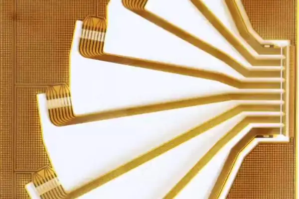
Actually, careful observation reveals the ingenuity of this technology everywhere. Why can those curved touchscreens on car dashboards fit so seamlessly into streamlined instrument panels? It’s thanks to the flexible circuit layer behind them. And the hinges of today’s popular foldable phones have densely packed gold lines that coordinate with the screen’s expansion and contraction each time the screen is opened—these are exquisite design details that ordinary consumers wouldn’t notice.
However, to be honest, I think the current applications are still too conservative. Since the material itself has stretchable properties, why not be bolder? For example, making the entire smartwatch strap into circuitry, or letting sensors on clothing move like fabric in the wind.
Recently, I saw that a laboratory is researching biodegradable flexible circuits, which is a new direction. Imagine how environmentally friendly it would be if disposable medical patches could decompose directly in the soil after use.
I firmly believe that technological breakthroughs often stem from the pressure from application-driven innovation. When designers dare to propose more imaginative concepts, supply chain companies like flexible PCB manufacturers are truly unleashed their innovative potential. After all, good materials science is always propelled forward by demand.
I recently chatted with a friend who works in smart hardware, and he mentioned that finding flexible PCB manufacturers is becoming increasingly difficult. It’s not that there are fewer manufacturers, but rather that people’s understanding of FPCs is still limited to “bendable circuit boards.” In reality, flexible PCBs are far more than just simple connectors.
I remember last year when our team was working on wearable devices, we discovered that simply replacing traditional circuit boards with flexible versions wasn’t enough. The truly interesting challenge was integrating sensors directly into the FPC. We tried integrating a heart rate monitoring module into the wristband, but the traditional approach didn’t work—either it was too thick, affecting comfort, or it caused severe signal interference.
Later, we changed our approach and directly commissioned a manufacturer to customize a flexible PCB with embedded sensors. This one-piece molding solution not only reduced the thickness by 0.8 millimeters but also solved the long-standing problem of connectors easily loosening. Looking back, the essence of flexible technology lies not in its “bendability,” but in how to integrate circuitry into the product structure.
I once visited a medical device exhibition and saw a temperature monitoring patch that attaches to the skin. Its FPC was as thin as paper, yet it integrated temperature sensing and data transmission functions. This design approach is more valuable than simply pursuing a high number of bends—when the circuit board becomes the functional carrier, the entire product’s form undergoes a qualitative change.
Many manufacturers are currently competing on whose FPC can be bent the most times, but I think this has missed the mark. The real discussion should focus on how to use integrated thinking, to make flexible circuitry the core of product innovation. For example, the curved control panel of a smart home system could completely replace the traditional button array with an FPC with touch sensors, simplifying assembly and improving reliability.
Several projects I’ve recently worked on are attempting to print biometric modules directly onto flexible circuits.
This highly integrated approach may completely change the form of wearable devices—we might not see watches or bracelets anymore,
This highly integrated approach may completely change the form of wearable devices—we might not see watches or bracelets anymore, but rather a second “electronic skin” that fits closer to the skin.
However, to realize this vision, manufacturers need to move beyond OEM thinking.
Currently, very few FPC manufacturers are willing to collaborate from the design stage; most still wait for customers to provide drawings.
But the biggest taboo in flexible design is simply applying the rigid board approach.
This is like using the logic of car manufacturing to build drones—it’s destined to miss real innovation opportunities.
I recently chatted with some friends who work in smart hardware and found that many people’s understanding of flexible PCBs is still at the stage of “as long as it can be bent, it’s fine.” In fact, flexible circuit boards are far more than just bending.
Choosing the right material is a crucial step. Common flexible substrates on the market include polyimide and polyester film, but the materials provided by different manufacturers vary greatly in heat resistance and flexibility. Some manufacturers use inferior substrates to reduce costs, resulting in products that quickly delaminate under high temperatures. Good FPC manufacturers do a lot of unseen work on material formulation, such as adjusting the thickness of the adhesive to control the overall flexibility.
I remember last year when our team was designing a wearable device, we encountered a problem with circuit breakage in the bending area. Later, we switched to an experienced flexible PCB supplier who recommended using a grid-like trace design in critical bending areas instead of traditional straight traces. This small change more than tripled the product’s lifespan.
Many electronic products now strive for thinness and lightness, placing higher demands on the thickness of flexible circuit boards. Excellent manufacturers can achieve ultra-thin designs of less than 0.1mm while maintaining circuit stability. This requires extremely precise etching processes.
I particularly admire manufacturers who are willing to invest in research and development. They are not content with standard products but instead adjust process parameters according to the specific application scenarios of their customers. For example, flexible PCBs used in medical devices require higher reliability standards, while consumer electronics products place greater emphasis on cost control.
Recently, I came across a domestic manufacturer that has developed a unique product line of rigid-flex PCBs. This type of board provides stability in rigid areas while retaining the bending characteristics of flexible areas, making it particularly suitable for connectors requiring frequent insertion and removal. However, this process demands highly sophisticated lamination technology.
With the increasing popularity of foldable screen phones, the application scenarios for flexible PCBs are expanding. This brings with it stricter requirements for bending lifespan. Some high-end products can already achieve over 200,000 bending tests, a feat achieved through breakthroughs in both materials science and manufacturing technology.
When choosing a supplier, I usually start by checking the quality of their samples. Good flexible circuit boards have clean edges, and the cover film adheres tightly to the substrate without bubbles; these details often reflect a manufacturer’s quality control level.
The future of flexible electronics will undoubtedly move towards thinner and lighter designs. Some manufacturers are already developing stretchable circuit boards, which presents entirely new challenges for materials and manufacturing processes. As a designer, I look forward to seeing more innovative solutions emerge.
In fact, product development and supplier selection are similar; both require attention to detail. Sometimes, seemingly minor improvements can lead to a significant enhancement in the product experience.
By the way, if you’re also developing related products, I suggest communicating frequently with the supplier’s technical staff. Their accumulated practical experience can often help you avoid many design pitfalls.
Every time I see those flexible electronic product designs, I think about one thing—there’s a lot more to these seemingly simple bends than meets the eye. I’ve met some friends who work on flexible PCBs, and I know they face some truly headache-inducing problems every day.
I remember a friend who makes smart bracelets complaining to me that during testing, they found a problem at a certain bending point. They later discovered it was due to an improper choice of substrate, causing microcracks after repeated folding. These kinds of detail issues often only surface when the product is close to mass production, and solving them is extremely time-consuming. In reality, these microcracks usually originate from stress concentration points within the material and gradually expand into visible fracture zones under repeated mechanical movement. Engineers often need to use finite element analysis to simulate stress distribution under different bending radii, and then combine this with high-magnification electron microscopy to observe the crack initiation process in order to accurately pinpoint the root cause of the problem. Sometimes, it is even necessary to readjust the circuit layout to avoid overly dense wiring in bending areas.
Many products are now pursuing increasingly thin and light designs, which places higher demands on flexible circuits. For example, the FPC in the recently seen rollable screen concept phone not only needs to be stretchable but also needs to ensure stable signal transmission; striking this balance is indeed difficult. Especially in high-frequency signal transmission, the impedance matching of flexible circuits can drift with deformation, potentially leading to a decrease in signal integrity. Some manufacturers have begun to use a grid-like grounding layer design or to place a shielding layer around critical signal lines, but this increases the thickness and stiffness of the FPC, creating new contradictions.
I have noticed that leading flexible PCB manufacturers are now focusing on material innovation, such as developing new cover film materials and more durable conductive adhesives. These seemingly small improvements can often extend the product’s lifespan by several levels. For example, the temperature resistance of polyimide substrates has increased from 260℃ to over 400℃, enabling FPCs to withstand more extreme welding processes. Conductive adhesives have evolved from traditional epoxy resin systems to composite materials containing silver nanowires, maintaining over 95% of their initial conductivity after tens of thousands of bends.
The automotive electronics sector also has unique requirements for flexibility. Unlike the frequent bending of consumer electronics, automotive-grade FPCs prioritize long-term stability. For instance, the wiring in steering wheels must withstand temperature changes and vibrations, presenting a different challenge for manufacturers. These products typically undergo aging tests simulating up to 15 years of use, including thousands of temperature cycles between -40℃ and 125℃, and continuous vibration tests at specific frequencies. Corrosion protection at connector interfaces is also crucial, often employing thicker gold plating to cope with the humid environment inside vehicles.
Applications in the medical device field may be the most demanding in terms of technical capabilities, especially for devices that need to be implanted in the human body. Flexible circuits must pass rigorous biocompatibility tests and achieve complex functions within limited space, requiring manufacturers to have extensive experience. For example, the thickness of the FPC inside a pacemaker must be controlled within 0.1mm, and it must be able to withstand long-term corrosion from the internal environment. Some special applications even require the circuit materials to degrade naturally in bodily fluids after completing their function, which places extremely high demands on materials science.
In fact, many innovations are currently limited by materials technology. For example, while transparent FPCs sound cool, they still face many obstacles in practical applications. Sometimes technological progress is not achieved overnight; it requires the joint efforts of the entire industry chain. Transparent conductive materials such as ITO (indium tin oxide) have brittleness issues, while emerging silver nanowires face the problem of high haze. More importantly, transparent substrates often have poor heat resistance, making them unsuitable for conventional SMT (Surface Mount Technology) processes, necessitating the development of entirely new low-temperature soldering systems.
What I find most interesting is the significant difference in understanding flexibility across different industries. Some pursue the ultimate number of bends, some value environmental adaptability, and others focus on miniaturization. This diversity precisely illustrates the broad prospects of flexible technology. The industrial robotics field requires FPCs to withstand dozens of continuous movements per minute, while aerospace applications focus more on the performance stability of materials under radiation environments. This demand for differentiation has prompted manufacturers to develop modular technical solutions, such as customizing different levels of flexibility by adjusting substrate thickness, copper foil type, and cover film combinations.
Watching flexible circuits evolve from simple connections to support a variety of cool products over the years, one can’t help but marvel at the vast amount of potential in this field. Each technological breakthrough can lead to unexpected application scenarios.
I’ve always felt that many electronic products are too rigid. Do smartphones have to be perfectly square and tablet-like? The emergence of flexible PCBs has given designers far more possibilities. I remember last year I disassembled the internal structure of a smart bracelet and found that it used three layers of bent circuit boards to achieve such a small layout. This design would have been impossible five years ago. This multi-layer stacking technology not only saves space but also enables the integration of complex functions, such as simultaneously placing sensors, antennas, and microprocessors on the same flexible board, greatly increasing the product’s functional density.
Choosing a reliable flexible PCB manufacturer is crucial. Once, our team, in order to meet a deadline, found a manufacturer with a very low price. However, when the sample arrived, we discovered cracks at the bends, and we had to re-produce it, which delayed us by two weeks. Good manufacturers have unique experience in material selection and processing. For example, they know where to increase copper foil thickness or how to arrange traces to withstand repeated bending. They might use polyimide substrates instead of ordinary FR4 material, which maintains stability in high temperature and humidity environments, while optimizing etching processes to reduce stress concentration points.
Now even car steering wheels are using flexible circuitry. Traditional rigid PCBs simply cannot fit curved surfaces, while flexible designs can perfectly wrap around the entire steering wheel frame while integrating buttons and touch sensing functions. This application has extremely high reliability requirements, as it involves driving safety. Manufacturers must pass rigorous vibration and high-temperature tests. For example, they need to simulate the steering wheel experiencing temperature differences from -40°C to 85°C in extreme weather conditions to ensure that the circuitry will not fail due to thermal expansion and contraction, and also verify durability through millions of bending tests.
I’ve noticed that some manufacturers are starting to offer design verification services, which is really useful. They will simulate the stress on the circuit board in actual use based on your product structure, telling you which areas are prone to problems. This early intervention is much more effective than post-treatment, avoiding many potential quality issues. Specifically, they use finite element analysis software to simulate the tensile deformation of circuit boards during assembly, and even conduct physical verification through 3D printed prototypes to help customers optimize connector positions and fixing methods.
Future wearable devices will undoubtedly be thinner, lighter, and more contour-fitting to the human body, placing higher demands on flexible electronics technology. I think the next breakthrough may lie in material innovation, such as developing substrates with better elasticity or conductive inks with greater bend resistance. PCB manufacturers that focus on R&D will be more competitive. Currently, laboratories are testing graphene composite conductive materials, whose bending life can reach more than ten times that of traditional materials, while achieving micron-level circuit precision, which is particularly important for developing medical-grade implantable devices.
In fact, the significance of flexible technology goes beyond electronic products themselves; it is changing the way we interact with technology. When circuits can be bent freely like fabric, the entire industrial design approach will change—this may be the greatest value brought by flexibility. For example, the hinge of a foldable tablet uses a special mesh wiring design, allowing the circuit to remain unobstructed even when repeatedly folded. This design thinking is giving rise to entirely new product forms.
In the field of industrial automation, people often pay attention to AI
Ever wonder how your phone maintains a stable signal? It relies on
When selecting components for a security monitoring system, most attention goes to
- Expert på produktion av små till medelstora serier
- Kretskortstillverkning med hög precision och automatiserad montering
- Pålitlig partner för OEM/ODM-projekt inom elektronik
Öppettider: (mån-lör) från 9:00 till 18:30