
Industrial Automation PCB Reliability: How to Achieve 10+ Years of Stable Operation
In the field of industrial automation, people often pay attention to AI
I’ve recently been wondering about something – why are more and more power supply designs now favoring thick copper PCBs? This needs to be discussed from a practical application perspective.
I remember a situation I encountered last year when I was helping a friend modify an audio amplifier. The original ordinary PCB always overheated at peak power. After switching to a heavy copper PCB, the effect was immediate – the temperature dropped by more than ten degrees Celsius at the same power output. The key lies in the heat dissipation advantages brought by the thick copper layer.
Many people think that thick copper design is simply about increasing the thickness of the copper foil. It’s not that simple. When current passes through a conductor, it generates heat – everyone knows that, right? But many people don’t realize that the rate of heat accumulation is much faster than imagined.
I saw a very interesting example: a manufacturer of industrial equipment increased the lifespan of their control board by more than three times after changing the power layer from a conventional thickness to a heavy copper structure. The reason is simple – the thicker copper layer not only reduces impedance but also significantly improves heat conduction performance.
Speaking of this, I have to mention a common misconception – some people think that using thick copper solves all problems. In reality, if the design is improper, it can lead to new problems, such as poor lamination or drilling difficulties.
Once, when visiting a factory, I saw that their process for handling thick copper boards was very meticulous – from the selection of base materials to the etching parameters, everything had to be specially adjusted to ensure the quality of the finished product.
Now, thinking about it, why do high-power devices prefer this design? Because when the current reaches tens of amperes, the conductive cross-section of ordinary PCBs is simply insufficient, while thick copper boards can easily handle this demand.
However, these boards are indeed significantly more expensive than ordinary PCBs, so the choice should be based on actual needs. For low-power devices, it may not be necessary to incur this extra cost.
My own experience is that when your design involves currents exceeding 15 amperes or has special heat dissipation requirements, it’s worth considering a thick copper solution. After all, the value brought by improved reliability often far outweighs the increased cost.
Recently, I’ve noticed an interesting phenomenon – even some consumer electronics are starting to experiment with localized heavy copper designs, especially in fast-charging circuits. This shows that the pursuit of power density is truly endless.
Ultimately, the choice of PCB structure depends on the specific application scenario; you shouldn’t blindly follow trends. But understanding the characteristics of various solutions is always a good idea; you might need them someday.
I’ve seen many people think that making thick copper boards is just about piling on more material, but this idea is too simplistic. Those who have actually worked with heavy copper PCBs know that it tests the coordination of the entire process, not just simply increasing the copper thickness. Once, when we tried to make a 12-ounce board, we encountered problems during the drilling process. Ordinary drill bits simply couldn’t handle it; they wore down significantly after drilling just a few holes. We later solved the problem by using special carbide drill bits – these details are often overlooked by beginners.
The lamination process is also a common pitfall. I remember once, in pursuit of efficiency, we directly used a standard pressure curve for lamination, resulting in noticeable delamination at the edges of the board. We later discovered that this was due to the excessive stress caused by the thick copper, requiring a multi-stage pressure application method to allow the resin to flow and fill properly. This lesson taught me that sometimes, slower is actually faster.
The choice of resin is also crucial. The resin content of ordinary board materials is simply insufficient to fill the deep grooves between the thick copper traces. We once tried using prepregs with a high resin content, but due to improper pressure control during lamination, the dielectric thickness was uneven. We later adjusted the formula to find a balance – ensuring sufficient filling without affecting structural strength.
In fact, the most interesting thing about making thick copper boards is seeing the interaction between the materials. For example, the difference in thermal expansion coefficients between copper and resin is a point worth considering. Once, a customer reported that the circuit board developed micro-cracks after reflow soldering. After investigation, we found that it was caused by stress concentration due to an excessively fast cooling rate. Now we specifically control the cooling curve. This seemingly simple adjustment can prevent major problems.
These experiences have made me realize that making thick copper PCBs is more like cooking; the temperature, ingredients, and every detail affect the final result. Simply piling up materials can easily backfire. The key is to understand the principles behind each process step so that you can produce boards that are both reliable and practical.
I’ve tinkered with thick copper boards a few times myself before I understood one thing – sometimes, the more you try to precisely control something, the more likely it is to go wrong. Take the etching process, for example. Many people think that as long as the chemical solution ratio is correct, everything will be fine. In reality, the factors that truly affect the accuracy of the pattern are often those invisible details. I encountered a board where the sampling tests were all successful according to standard procedures, but during mass production, fluctuations in temperature and humidity in the workshop caused burrs on the edges of the lines.
The most troublesome aspect of heavy copper PCBs is not the thickness itself, but the uniformity. It’s like baking a cake; the surface looks golden and crispy, but when you cut it open, the middle is still wet dough. Once, to meet a tight deadline, we skipped the thickness inspection of the intermediate layers and went directly to the pattern transfer stage. As a result, the impedance values of the entire batch of boards fluctuated wildly.
In fact, many manufacturers now focus on etching precision but neglect the stability of the material itself. I’ve seen people use the most expensive equipment for heavy copper processing, but if the ductility of the copper foil in the base material is not up to standard, the resulting line cross-section will still be trapezoidal. It’s like cutting butter with a blunt knife; no matter how careful you are, you can’t cut a perfect right angle.
The truly reliable approach is to perform microscopic sampling from the first process step, not waiting until the boards are laminated before thinking about measuring the thickness. An experienced master taught me a little trick: before electroplating, use a microscope to observe the crystal orientation of the copper foil. Sometimes, a difference of a few degrees in the lattice arrangement can result in more than double the difference in the penetration speed of the etching solution.
Recently, we tried a dynamically adjusted etching scheme, not blindly pursuing perpendicularity, but designing the line profile shape according to the current load requirements. For example, in areas requiring high current, the top is made slightly wider, like a small platform, while the signal line areas prioritize edge clarity. This approach actually increased the yield rate by 30 to 40 percent.
Ultimately, thick copper technology isn’t about who has the most advanced equipment, but about who can connect the variables in each step of the process and think holistically. It’s like a traditional Chinese medicine doctor feeling the pulse – they need to understand the rhythm of blood and energy flow; focusing on just one indicator when prescribing medicine will inevitably lead to problems.
I’ve recently been thinking about circuit boards, and it’s quite interesting. I used to think PCBs were just basic foundation components – until I used a heavy copper PCB for a project and realized that wasn’t the case at all. At that time, to power high-power equipment, I tried using regular boards, and almost burned out the components. Only after switching to a thick copper PCB did I understand that this thing is essentially an extension of the cooling system.
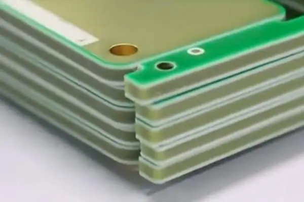
Have you ever seen the scene of an old electric heating element glowing red? When the current is too high, the copper foil on a regular circuit board is similar to that state, while a thick copper design is like building an eight-lane highway for the current. I remember once disassembling an industrial frequency converter and seeing a three-layer stacked heavy copper PCB cross-section that looked like a sandwich cookie. This structure not only distributes the current load but also spreads the heat evenly, which is much smarter than simply adding heat sinks.
Speaking of material selection, many people’s first reaction is to focus on thermal conductivity, but the key is actually thermal expansion matching. Once, I used a ceramic substrate to build a high-frequency circuit. At first, I thought the fast heat dissipation would make it stable, but after ten minutes of operation, I heard cracking sounds – the thermal expansion coefficients of the ceramic and metal were too different, causing it to crack. The problem was only solved by switching to a composite substrate.
Now, high-end power devices seem more like playing a materials puzzle game. The conductive layer needs to be thick enough, the insulating layer needs to be tough enough, and the substrate needs to withstand thermal cycling. Sometimes I even feel like we’re not drawing circuit diagrams, but designing miniature buildings – considering where to place load-bearing walls and how to design ventilation ducts. The automotive inverter I saw recently directly made the heavy copper PCB into the shape of a heat sink fin; this approach is particularly clever, allowing every square centimeter to perform two functions simultaneously. What surprised me the most is that now even ceramic substrates can have copper conductors directly embedded in them, like making latte art, printing metal paste onto green ceramic sheets and sintering them together. This approach preserves the insulation and heat resistance of ceramics while avoiding welding stress problems. Although the cost is higher, it’s a life-saving design for aerospace equipment.
The longer I work with power electronics, the more I realize that we are constantly negotiating with various physical laws. Joule heating needs to be managed, electromagnetic interference needs to be controlled, and even airflow needs to be considered. Once during testing, I found that simply changing the capacitor placement could lower the entire board temperature by seven or eight degrees. These kinds of details aren’t found in textbooks.
If silicon carbide devices become widespread in the future, current thick copper technology will likely need to be upgraded, because eddy current losses will become a new problem as switching frequencies increase. But it’s also exciting to think about; this continuous process of negotiating with physics is the greatest joy for engineers.
I’ve been thinking about something recently—why are more and more engineers starting to pay attention to those seemingly very thick circuit boards? Especially when we discuss applications that require handling high currents.
I remember a project last year that left a deep impression on me. We needed to design a power module that could withstand high current surges. At first, some team members suggested using a stacked multi-layer board solution to solve the heat dissipation problem. But later we found that this approach was actually a dead end.
That experience taught me a lesson: when the current reaches a certain level, the saying “quantitative change leads to qualitative change” is particularly applicable in the field of circuit design. Ordinary circuit boards may perform well in low-power applications. But when it comes to scenarios that require carrying tens or even hundreds of amperes of current, the situation is completely different.
I’ve seen many novice engineers fall into a misconception—thinking that simply widening the trace width can solve high-current problems. In reality, this is far from enough.
What truly tests the performance of a circuit board is its stability under continuous high-load operation.
Once I visited an industrial equipment manufacturing plant and saw the circuit boards used in their equipment control cabinets, which inspired me greatly. Those boards looked much thicker than ordinary circuit boards. Later I learned that they were special boards designed specifically for heavy-duty applications.
The advantage of this type of board is that it can better dissipate heat, preventing localized overheating that can lead to component damage. This stability is especially important in equipment that needs to run for extended periods. Many applications in the new energy field now demand higher performance from circuit boards, such as electric vehicle charging systems or solar inverters. These devices often need to maintain stable operation in harsh environments.
I believe the future direction of circuit board technology will focus more on the inherent properties of the materials themselves, rather than just optimizing wiring methods. After all, when the current reaches a certain level, the conductivity and heat dissipation of the material become the decisive factors.
I recently chatted with a friend who designs power supplies, and he mentioned that many high-power applications are now using thicker copper foil to make circuit boards. This made me realize that technological progress often happens this way—when traditional methods encounter bottlenecks, people look for more fundamental solutions.
Sometimes the simplest solution is the most effective, especially when dealing with fundamental but critical issues like high current. Instead of spending too much effort on complex wiring techniques, it’s better to choose a more suitable substrate from the beginning.
When designing high-power electronic devices, I’ve increasingly realized that simply adding heat sinks doesn’t solve the fundamental problem. Many people immediately think of adding heat sinks, but they overlook the crucial role the PCB itself plays.
I remember once debugging a power module, and I found that even with a large aluminum heat sink, it still overheated. Later, I replaced the ordinary board with a heavy copper PCB, increasing the copper thickness to 4 ounces, and the temperature dropped by fifteen degrees. This thick copper layer is like giving the circuit board a thermal undershirt—but in this case, it’s to quickly conduct heat away. The large area of copper foil quickly dissipates localized hot spots, preventing any single component from enduring excessive heat.
The choice of connectors is often underestimated. In one test, ordinary pin headers melted under prolonged high current. It only stabilized after switching to specialized high-power connectors. These connectors require consideration of not only the rated current but also the contact area and material. I usually reinforce the connector pads with a group of vias, like riveting the socket, to prevent the copper foil from peeling due to repeated insertion and removal.
Regarding electromagnetic interference, my experience is that it’s better to do physical isolation during the layout phase than to deliberately segment the ground plane. In one project, the sampling circuit was placed next to the IGBT, and the signal jumped like an electrocardiogram. Later, rearranging the layout so that the power lines and signal lines were on separate sides significantly improved the situation.
What surprised me the most was the effectiveness of thermal vias. Once, I imitated someone else’s design and drilled a neat array of vias at the bottom of the chip, but temperature measurements showed that it performed worse than randomly distributed vias. Later, I understood that heat conduction also needs to extend naturally, like the branching of a river.
Now, I feel it’s a pity to see those designs that stubbornly add more heat sinks. When you can make thick copper PCBs the main component of the heat dissipation system, you’ll find that many traditional heat dissipation problems have new solutions from a different perspective.
I’ve been thinking about something recently: why are more and more engineers becoming so fond of heavy copper PCBs? The answer is actually simple – when our designed equipment needs to handle high currents, ordinary circuit boards simply can’t withstand the pressure. I remember last year when I helped a friend modify a solar controller, I found that a regular PCB couldn’t even last half an hour under full load before the traces started to overheat and deform. That’s when I truly realized that current carrying capacity isn’t just a theoretical number game, but a real engineering challenge.
Some might ask, wouldn’t adding more parallel wires work? But in practical applications, there’s often not enough space for that. For example, the charging modules of electric vehicles or the power supply units of industrial machine tools have layouts as compact as a jigsaw puzzle; this is where the value of heavy copper PCBs becomes apparent. It doesn’t need to rely on quantity; simply increasing the copper foil thickness allows the current to flow smoothly. I’ve seen boards with 6-ounce copper thickness operating at temperatures more than ten degrees lower than traditional designs under continuous high voltage. This difference directly impacts the equipment’s lifespan.
However, the manufacturing process of heavy copper PCBs is indeed much more complex than ordinary circuit boards. Once, when I visited a factory, I saw workers handling 8-ounce base materials with the care of handling a work of art, because the excessively thick copper layer is prone to side etching problems during the etching process. Moreover, thickness differences during multi-layer board lamination can lead to uneven distribution of the dielectric layer; these details all affect the final performance. But then again, when you see the finished product stably transmitting hundreds of amperes of current, you’ll feel that all the initial trouble was worth it.
Many industries are quietly upgrading their materials, such as in data center servers, power supplies, and rail transit traction systems, where reliability requirements are extremely stringent. Traditional designs might have been adequate in the past, but heavy copper PCBs bring not only performance improvements but also a fundamental shift in design philosophy.
We are beginning to learn how to use the physical properties of materials to solve engineering challenges, which is far more intelligent than simply piling up components.
Seeing everyone discussing high-power circuit design, I’d like to share my experiences. Many people think of using thicker copper foil whenever they encounter high currents. It’s true that thick copper PCBs can handle larger currents.
However, I think there’s a misconception worth noting—simply increasing copper thickness isn’t necessarily the optimal solution. Once, when testing a heavy copper PCB, I observed an interesting phenomenon: although the copper layer was thickened by 30%, the actual current carrying capacity only increased by less than 15%. Later, I discovered that the heat dissipation design wasn’t adequate, and the heat buildup actually limited performance.
The impact of PCB layout on current distribution is more subtle than we imagine. I remember a motor driver board that repeatedly experienced localized overheating.
Later, adjusting the routing angle of the critical paths by 10 degrees reduced the temperature by 8 degrees Celsius. Sometimes, fine-tuning the routing is more effective than simply increasing copper thickness.
Resistance control is quite interesting.
I’ve seen people widen all the traces to reduce resistance.
As a result, the board area increased by one-third.
In fact, in multilayer boards, rationally planning the current paths often yields better results with less effort.
Some designs now rely too much on simulation software, neglecting actual operating conditions. Once, the temperature rise curve measured in the lab differed from the simulation results by nearly 20%.
Later, it was discovered that the dead air zones inside the enclosure hadn’t been considered. The gap between theory and reality.
Perhaps more practical testing is needed to bridge this gap.
Speaking of inverters in new energy vehicles, I think heat dissipation is the real bottleneck.
I’ve seen too many cases where inadequate thermal management led to reduced performance.
Instead of endlessly increasing the copper layer thickness, it’s better to put more effort into the heat dissipation channel design. After all, even with large currents, there must be a suitable heat dissipation path.
I’ve recently been studying a very interesting phenomenon: many people think that heatsinks and fans are the panacea when designing high-power circuits. In fact, the PCB itself can be a great help, especially those boards using heavy copper technology.
I remember noticing a detail when disassembling an industrial power supply: the copper foil on ordinary circuit boards was as thin as paper, and the heat couldn’t be dissipated at all. But with a board designed with a thick copper layer, the entire PCB acted like its own heat dissipation system. During one test, I deliberately touched and compared the temperatures of different boards, and the thicker copper board had a noticeably more uniform temperature distribution.
Now, when designing power circuits, I pay more attention to the copper foil thickness. Ordinary consumer electronics might be fine with 1 ounce of copper, but for applications like motor drives, using a PCB without thick copper is like walking a tightrope. Last time I helped a friend modify a drone’s ESC (Electronic Speed Controller) design, replacing the standard PCB with a heavy copper version resulted in an extra ten minutes of flight time.
Many people think that thickening the copper layer is only for handling larger currents. However, there’s also a hidden benefit: mechanical strength. I once saw a vibration test where the components on a standard PCB were shaking loosely, while the components on the thick copper board had much more secure solder joints. This reminded me why automotive electronics particularly favor this technology, as they need to withstand various bumpy environments.
However, thick copper technology isn’t something you can use indiscriminately. The substrate material must have a thermal expansion coefficient that matches the copper layer. I’ve seen examples of people blindly increasing the copper thickness, resulting in delamination and blistering.
Ultimately, choosing whether to use a heavy copper design is like choosing tires – ordinary tires are fine for city driving; but for off-road driving, you need sturdy off-road tires.
In the field of industrial automation, people often pay attention to AI
Ever wonder how your phone maintains a stable signal? It relies on
When selecting components for a security monitoring system, most attention goes to
- Expert på produktion av små till medelstora serier
- Kretskortstillverkning med hög precision och automatiserad montering
- Pålitlig partner för OEM/ODM-projekt inom elektronik
Öppettider: (mån-lör) från 9:00 till 18:30