
Industrial Automation PCB Reliability: How to Achieve 10+ Years of Stable Operation
In the field of industrial automation, people often pay attention to AI
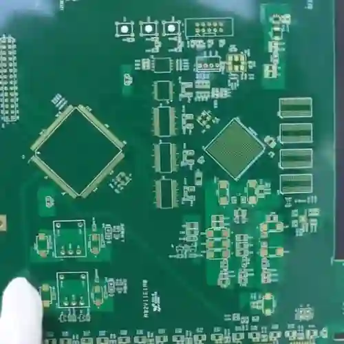
I’ve always felt that many people have a rigid understanding of 4-layer PCBs. It seems they think it has to be designed according to some fixed pattern, but it’s actually quite flexible. I remember when I first started in electronic design, I thought 4-layer boards were much more expensive than double-sided ones, but I later found that wasn’t the case at all.
Once, I was working on a small IoT sensor, and I initially wanted to use a double-sided board to save money, but I found that the signal interference was particularly severe. Switching to a 4-layer board solved the problem immediately. The key was placing the power and ground planes on the two inner layers, which freed up a lot of routing space on the outer layers and significantly reduced electromagnetic interference. This 4-layer structure is especially suitable for devices that require a compact size but also need stability.
Many consumer electronics products now use this design, such as smartwatches or small medical devices. The advantage of 4-layer boards is that they can achieve a better balance of performance in a limited space. I’ve seen some engineers try to save costs by using double-sided boards, only to end up spending more time on debugging later.
Ultimately, the choice of layer stacking depends on the specific requirements. If the signal lines are particularly dense, placing the two signal layers in the middle might be more suitable; if high electromagnetic compatibility is required, then signal integrity should be prioritized. Every project is different.
A recent car device project I helped a friend with is a good example. We initially planned to use a standard layer stacking scheme, but later found that adjusting the power plane to the third layer significantly improved heat dissipation. This kind of flexible adjustment is the true value of 4-layer PCBs. Ultimately, good design isn’t about rote memorization of standard solutions, but about making the most appropriate choices based on the actual situation. The charm of a 4-layer board lies in the greater design flexibility it offers.
I’ve always felt that many people misunderstand 4-layer PCBs—as if simply adding more layers solves all problems. In fact, the greatest value of upgrading from a double-sided board to a 4-layer board is the increased freedom in layout.
I remember an interesting phenomenon I encountered while helping a friend revise an audio processing board. They had crammed the analog and digital sections together on a double-sided board, resulting in significant noise. By switching to a 4-layer structure and placing the power plane in the middle two layers, we were able to dedicate the top layer to signal isolation.
Sometimes, I see novice designers rushing to fill every available space on a 4-layer board, which actually destroys the advantages of proper partitioning. For example, excessive copper pouring in the digital circuit area can increase parasitic capacitance, affecting signal edge speed. A more reasonable approach is to divide the board into regions based on signal type, such as concentrating clock lines in specific channels to avoid crosstalk with data lines.
The art of routing lies in understanding the importance of “white space,” and this is especially evident on 4-layer boards. For example, maintaining sufficient clearance around high-speed signal paths effectively reduces electromagnetic radiation and minimizes the risk of impedance discontinuities. This “white space” isn’t just about physical spacing, but also includes avoiding placing vias or cutting the reference plane directly beneath sensitive lines.
I usually place the most sensitive lines on the signal layer closest to the ground plane, so that even in the event of sudden interference, there’s a buffer. For example, prioritizing the routing of RF receiving paths or high-precision ADC input traces above the adjacent ground plane utilizes the mirror effect to create natural shielding. This layout reduces common-mode noise and improves signal integrity.
Once, while testing a motor driver board, I noticed a detail: when PWM signal lines and sensor feedback lines ran parallel for a long distance, even with ground plane isolation, slight coupling occurred. Changing to perpendicular routing eliminated the problem. This is because parallel traces form an implicit antenna structure, and even with a reference plane, high-frequency harmonics can still couple through the edge fields. Perpendicular routing minimizes the coupling area; tests showed this change reduced crosstalk by more than 15dB.
Many EDA software programs now display routing density in real time, a feature particularly useful for 4-layer boards because correcting routing errors on inner layers is much more difficult than on double-sided boards. For example, Altium Designer’s thermal mapping function can visually display areas where vias are concentrated, reminding designers to avoid creating via arrays under BGA chips that obstruct the continuity of the power plane. This preventative design can significantly reduce later modification costs.
Regarding the use of vias, I think it needs to be discussed on a case-by-case basis. For example, the number of vias should be strictly controlled in high-frequency sections, but appropriately increasing vias in the power section can improve current carrying capacity. The key is to understand the direction of current flow, not just blindly follow rules. For instance, in DC-DC converter layouts, at least 2-3 vias should be configured per ampere of current to disperse thermal effects, and the via anti-pad size should be adjusted according to the signal wavelength. For millimeter-wave frequencies, back-drilling is needed to control stub length.
Recently, while working on a project with a wireless module, I found that the heat dissipation advantages of 4-layer boards are underestimated. By hollowing out the ground layer on the back of the heat-generating chip and connecting it to the power plane, a natural heat dissipation channel can be formed, a flexibility difficult to achieve with double-layer boards. In the specific implementation, a thermal via array connects the chip’s thermal pad to the internal copper layer, and then an X-shaped division guides the heat to the heat dissipation pads on the board edge. Testing showed a reduction in junction temperature of more than 8°C.
In fact, good PCB design is like urban planning; it needs to ensure smooth main roads while also providing breathing space for smaller alleys. 4-layer boards give us more possibilities for dividing functional areas, but the final effect depends on how these spatial layers are used. For example, the second layer can be set as a complete ground plane as an electromagnetic shielding reference, the third layer can be divided into power areas according to voltage levels, and the top and bottom layers can implement differentiated trace width rules based on signal priority. This three-dimensional layout thinking is the core value of 4-layer boards.
I recently found several circuit board samples from different periods while organizing my studio. Looking at those early double-layer boards to the current multi-layer designs is very interesting. I remember when I first started working in electronic design, I always thought that 4-layer boards were too expensive and unnecessary, but now I feel that in some cases, not using them is a waste.
Once, I helped a friend modify a smart home controller. The original double-layer board always experienced signal interference in high-temperature environments. After switching to a 4-layer version, the problem was solved. The key was that the two middle layers were specifically used for power and grounding, which made the entire system much more stable. Many people think that only high-end equipment needs this kind of design, but in fact, using this structure in ordinary industrial control equipment or smart home products can reduce later debugging costs. I’ve encountered some engineers who like to use multi-layer boards even for simple circuits, which is sometimes unnecessary. However, for projects that require processing complex signals or have strict anti-interference requirements, spending a little extra on manufacturing can save a lot of trouble in later maintenance. Especially now, with components getting smaller and signal frequencies getting higher, the limitations of two-layer boards are becoming increasingly apparent.
There’s a common misconception that increasing layers is only for easier routing; in fact, the stability of power distribution is key. For example, in a temperature control system, current fluctuations during motor startup, if not handled properly, can affect the entire sensor reading, while a separate power plane can effectively buffer these sudden changes.
Of course, not all projects require multi-layer boards. For a simple LED controller I worked on recently, a double-sided board was more appropriate. The key is to consider the actual needs, not blindly pursue a higher number of layers. Sometimes I see designs that pile on layers to achieve certain parameters, resulting in increased costs but limited performance improvement. This balance requires practical experience.
I now make it a habit to evaluate whether a 4-layer structure is needed at the beginning of a project, because making changes to the layout later is very difficult, especially for high-frequency signals. The cost of re-routing might be higher than simply choosing a suitable basic design from the start.
Recently, while working on 4-layer PCB design, I realized that many people’s understanding of it is still superficial. The beauty of 4 layers lies in the extra design space it provides, like giving the circuit board a custom-tailored suit. I remember working on an RF project where the double-layer board was constantly plagued by interference problems. Switching to a 4-layer structure significantly improved the signal quality.
The layered design is particularly interesting; it’s not as simple as stacking building blocks. The inner layers can be dedicated to power and ground lines, while the outer layers focus on signal transmission. This division of labor significantly improves the efficiency of the circuit board. However, it’s important to note that 4-layer boards are more expensive than double-layer boards, but for complex projects, this investment is well worth it.
Once, I helped a friend modify a drone flight control board. The original double-layer design always had signal crosstalk issues. Switching to a 4-layer structure not only solved the interference problem but also reduced the board area by one-third. This change made me realize how important choosing the right number of PCB layers is for product optimization.
Now I see many newcomers immediately aiming for six or eight-layer boards, which I think is unnecessary. For most consumer electronics products, 4 layers are sufficient. The key is to properly plan the function of each layer.
Speaking of material selection, that’s also quite important. Different substrate thicknesses affect overall performance. For example, in applications requiring high-frequency signal transmission, using low-loss FR-4 material or higher-grade Rogers laminates can significantly reduce signal attenuation. Copper foil thickness not only affects current carrying capacity but is also closely related to impedance control.
I prefer using a 1.6mm thickness with 1-ounce copper foil; this combination strikes a good balance between cost and performance. Of course, the specific choice depends on project requirements. For example, in space-constrained wearable devices, a thinner 0.8mm substrate might be chosen to reduce overall thickness.
Sometimes I feel that designing circuit boards is like architectural design, requiring both structural stability and reasonable functional partitioning. For example, when placing components, heat dissipation paths must be considered, high-frequency signal lines should avoid right-angle turns, and sensitive analog circuits should be isolated from digital circuits.
The advantage of a 4-layer board is that it gives us enough flexibility to handle various complex situations. By setting up a complete ground plane layer, it not only provides a stable reference ground but also acts as electromagnetic shielding. The power layer can be designed into segmented areas to provide independent power supply for circuits with different voltage levels.
My recent smart home project fully demonstrated this. Through reasonable layer allocation, it not only achieved stable power management but also ensured the integrity of high-speed signal transmission. This experience further convinced me that choosing the right PCB structure is crucial for project success.
In fact, every project has unique requirements. For example, industrial control boards need to focus on anti-interference, medical equipment needs to consider safety, and consumer electronics need to balance cost and performance. During the design process, multiple factors such as signal integrity, power integrity, and thermal management need to be considered comprehensively.
Instead of rote memorization of so-called standard solutions, it’s better to calmly analyze the actual needs. After all, a good design is always a customized product. It’s important to utilize simulation tools for early verification and find the optimal solution through parametric analysis.
The feeling of satisfaction when seeing your designed board running stably is indescribable. Especially when the product passes various rigorous tests and is finally mass-produced and gains user recognition.
This is probably the joy of being an engineer – through meticulous layout and planning, bringing life to a cold circuit board. Every successful wiring optimization, every technical problem solved, witnesses the tangible manifestation of design thinking.
In the field of industrial automation, people often pay attention to AI
Ever wonder how your phone maintains a stable signal? It relies on
When selecting components for a security monitoring system, most attention goes to
- Expert på produktion av små till medelstora serier
- Kretskortstillverkning med hög precision och automatiserad montering
- Pålitlig partner för OEM/ODM-projekt inom elektronik
Öppettider: (mån-lör) från 9:00 till 18:30