

HBM Memory PCB Manufacturing Challenges: How to Vet HDI and Multilayer Suppliers for Warpage, Micro-Via, and Heavy Copper Risks
Building a board around HBM is harder than the datasheet suggests. Learn
A gas leak detector is only as trustworthy as the board under its sensor. The sensor front end handles nanoamp-level currents and microvolt-level differential signals, so surface leakage in humid air, flux residue, ionic contamination, moisture absorption of the laminate, dielectric thickness variation and heat from nearby parts can shift a baseline long before an op-amp specification matters. This article collects first-hand lessons on a Gas Leak Detector PCB: why humidity leakage dominates op-amp bias current, why guard rings and isolation do not replace clean laminate and cleaning, when HDI helps and when a plain multilayer board is better, how catalytic bridge symmetry is limited by copper and dielectric dispersion, and how intrinsic safety rules, derating, thermal paths and probe-induced noise interact with the layout. It also explains how to question an HDI or multilayer PCB supplier by moisture data, insulation resistance, cross-sections and batch impedance data. A short FAQ follows at the end.
I have worked on gas detection equipment hardware for several years, and I increasingly feel many people put their energy in the wrong place. Everyone starts by discussing how to choose the sensor and how to configure the op-amp, as if the project were stable once the front-end circuit works. But what really makes a gas alarm overturn on site is often that most unremarkable Gas Leak Detector PCB. However well the sensor performs in the lab, once it is mounted on a board with an unstable process, all kinds of strange problems appear in a humid site with large temperature swings.
I remember a project making a fixed combustible gas detector: there was no problem at all at the prototype stage, small-batch trial production was passable, and then, after being shipped to the southern coast, false alarms were reported by customers one after another in less than half a year. We checked all around, and the sensor itself was fine; the problem lay in PCB surface leakage. That batch of boards used ordinary solder mask and ordinary surface finish, and the field humidity stayed at eighty or ninety percent for a long time. The signal at the front end of a gas sensor is weak to begin with, and with a little ionic residue on the board surface activated by moisture, the leakage current directly pushed the baseline off. Later we changed to another multilayer pcb supplier, changed the laminate to a low-water-absorption one, and also specially adjusted the solder mask and surface finish, and only then did the problem slowly come down. Since then I have never dared to specify a supplier casually at the mass production stage.
I have also gone to the other extreme. Later I made a portable four-in-one detector with tight internal space, where the sensor, battery, buzzer and display were all crowded into one small shell. My first reaction at the time was that such an industrial product did not need HDI, and a double-sided or four-layer board could be forced in. But when I actually did it I found that once space is compressed to a certain point, routing and component placement simply cannot be turned around, and in the end I was forced to redesign with an hdi pcb manufacturer. The reliability of laser microvias is actually better than imagined; the key is to watch hole copper thickness and via-fill quality afterward in mass production. Gas detectors are often carried on the body and cannot escape drops, vibration and temperature cycling, and if the microvias of an HDI board have stress concentration, hidden fractures may appear after some time of use, and this kind of fault is very hard to troubleshoot on site.
Speaking of multilayer pcb manufacturers, my habit now is first to see whether they have made industrial detection boards, not only to look at the quotation and line width and spacing capability. Some factories are very good at consumer electronics boards and have beautiful process parameters, but they have no concept of low leakage, moisture resistance and conformal coating compatibility. You stress to them that the gas sensor signal is very weak and surface ionic contamination must be controlled, and they say they know, but the board made is still built to ordinary consumer standards. Everything is normal at the sample stage, and problems arrive once the batch goes up. So I now prefer to cooperate with manufacturers who have long made industrial control and instrumentation PCB, even if it costs a bit more, and I feel it is worth it.
The catalytic combustion sensor also taught me a lesson. This sensor is itself a Wheatstone bridge, and zero stability depends a great deal on the matching of the compensating elements. But one batch of our boards showed obvious zero drift in mass production, and at first we suspected a sensor batch problem; later we found that the copper thickness and line width tolerances of the two bridge arms on the PCB had not been controlled. Different multilayer pcb suppliers differ greatly in their control of inner core and plating uniformity, and traces that look symmetric on the design drawing may actually come out with impedance off by a tiny amount. For ordinary digital circuits this does not matter, but for a millivolt-level differential signal like this it is enough to give you a headache.
So if someone asks me now how to get started with gas detection hardware, I will not advise him to first gnaw at the sensor specification sheet or rush to choose an MCU. I will advise him to think the PCB matter through first: find a reliable hdi pcb supplier or multilayer board supplier and pin down the board material, solder mask, surface finish, impedance tolerance and via filling one item at a time. The sensor decides which gas you can measure, but the stability of the Gas Leak Detector PCB decides whether the data you measure can still be trusted three years later. A pretty waveform in the lab is only a starting point; whether it stays stable on site is the real value of this board.
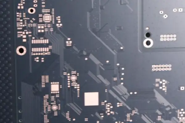
What I have felt most deeply in the years of making gas leak alarms is that many people start by staring at sensor selection and amplifier circuit noise and treat the PCB itself as a passive carrier. In fact the Gas Leak Detector PCB is far more sensitive than an ordinary digital control board: the sensor front end is often an extremely weak current or voltage change, and board surface contamination, solder mask residue, interlayer leakage and even fingerprints can carry the baseline away. Once this kind of physical-level interference enters mass production, investigation is very painful, because on the oscilloscope you simply cannot see one obvious fault point, only a slow drift in the reading.
After dealing with several hdi pcb manufacturers, I found that their understanding of gas detection products differs greatly. Some manufacturers only care how fine the line width and spacing can go and do not ask you why you want an HDI structure. My own experience is that the greatest meaning of HDI here is not making the board small but that laser blind vias and thinner dielectric layers can separate the analog front end from the digital part more cleanly. If the hdi pcb supplier you choose does not control via-fill uniformity and interlayer registration accuracy well, then these tiny geometric deviations become parasitic capacitance differences on the signal path and finally show up in the consistency of sensor readings.
The situation is even more obvious with multilayer boards. I once made a four-layer version in which analog ground and digital ground were split, but the return path was cut into pieces by vias, and the sensor output had a periodic jump all the time. Later I changed to six layers and found a multilayer pcb manufacturer specializing in industrial products to redo the layout, putting the sensor front end on an inner layer right next to a complete ground plane, and only then did the problem truly stabilize. This made me realize that a multilayer pcb supplier cannot be treated only as a processing step: their lamination parameters, dielectric thickness tolerance and inner-layer pattern position accuracy all affect how the board behaves at different temperatures and humidities. In other words, the design drawing is only an ideal state, and the actual finished product is turned into physical reality by the supplier’s process capability.
The CE certification gate is also very real. Many people think CE is mainly about preparing documents and writing a declaration, but once you actually go to the test house you understand that the reviewer will measure your creepage distances and clearances with calipers and look at the insulation slots, coating and component spacing on your board. Especially for combustible gas detection products, the physical structure directly decides whether certification can pass. I once experienced an insulation test failure because a certain capacitor was too close to the metal housing, and in the end I could only revise the board and cut slots again. After that I realized that CE is not a matter of supplementing documents at the end; it is embedded in every millimeter of physical space from the layout stage.
Now back to the sensor itself. Electrochemical, catalytic combustion and infrared each have their own temper, but what they share is that they are extremely sensitive to PCB parasitic effects. If the traces near the sensor are too long, or adjacent layers carry high-speed digital signals, these couple in through capacitance. What really tests the skill on a Gas Leak Detector PCB is not routing the lines through but blocking those invisible coupling paths one by one. Many young engineers are used to pouring a complete ground plane first and then routing, but a gas detection front end sometimes needs local clearance or single-point grounding, and blindly pouring copper actually leads interference to sensitive nodes.
So my overall judgment is that the difficulty of this kind of board has never been the selection of a particular component but physical consistency. HDI and multilayer board suppliers can help you solve structural density and interlayer control, but the premise is that you have thought clearly about your own sensor characteristics, temperature drift paths and CE boundaries. Otherwise even the best hdi pcb supplier is only processing to the drawing and cannot bear for you the physical risks left in the design stage. After the board is made, those neglected details slowly appear on site, and often at the most inconvenient time.
After several years in gas detection equipment, I have a feeling that may go against many reference designs: the bias current of the op-amp in a gas sensor front-end circuit is over-discussed. Nowadays any CMOS op-amp can have an input bias of a few tens of pA or even lower, which is nothing compared with the several tens of nA output of the sensor. What really gives me a headache is the leakage current of the Gas Leak Detector PCB itself in a humid environment, which is often much larger than the op-amp bias.
There was a batch of boards whose op-amp bias was rated at only a few pA, but when the humid damp season came the zero point drifted badly. Investigation later found that the trace spacing was too close and, together with moisture absorption of the solder mask material, leakage occurred between the sensor WE node and the adjacent trace, forming an extra nA-level current path. This current was superimposed directly into the measurement loop, with an influence more than an order of magnitude larger than the bias current. So later, when choosing a multilayer board supplier, I specifically ask them to report the solder mask material and minimum line spacing, especially the treatment around the sensor’s sensitive nodes.
The programmable transimpedance resistor design mentioned in the original text, I have tried too, and I do not like it much. The switched capacitors and charge injection inside a programmable resistor bring spikes when the gain is switched, and if the gas concentration happens to change quickly, that transient error is hard to filter out completely by software. In batch products I prefer fixed resistors with analog switches to select among several resistance ranges, so at least the switches are external and I can control the layout and drive timing myself. For the programmable resistor integrated in a chip, many details are not under control, and when something goes wrong you can only stare helplessly.
When cooperating with an hdi pcb manufacturer, I repeatedly stress that a guard ring must be made around the sensor input pin, but some manufacturers do not understand the electrochemical front end well enough and only build it as an ordinary digital circuit. A guard ring that is not truly driven to the same potential is useless if you merely draw a circle. Once I found a consumer-electronics hdi pcb supplier whose process was very advanced but who did not understand the particularity of nA-level current measurement at all, and the boards that came out had test point residue next to the sensor pin, which directly became a leakage channel.
If a multilayer board manufacturer has insufficient experience, stackup planning also affects signal integrity. My habit is to put the sensor analog ground on a separate layer, further from the digital ground, to avoid digital back-injection. For many ordinary multilayer pcb manufacturers this requirement needs extra communication, because by default they pour the ground plane over the whole layer, which in fact leads interference into the analog area. So before cooperating now I always send a layout constraint note first, stating clearly which areas must not have copper pour and which nodes need protection.
For current measurement, my experience is not to stare only at the bias index on the op-amp datasheet. That number is measured at a specific temperature, whereas the actual working temperature range of the board may reach above 60 degrees, and bias rises exponentially with temperature. Even so, going from a few tens of pA to a few hundred pA is only a zero-point issue for a sensor with several hundred nA output and can be calibrated away by software. The real random error comes more from the temperature coefficient of the transimpedance resistor itself and the long-term drift of the reference voltage, which are instead easily overlooked.
When choosing a multilayer pcb supplier, I now give priority to whether they have made analog small-signal or medical electronics boards. Those who have will understand why you require solder mask openings, why you do not let them add test points, and why you pull the line spacing to twice the normal. A supplier who has not, however high-end the process, may make a board that makes your front-end current reading mysteriously gain a few nA, and then you have to spend weeks locating it.
Broadly my view is this: the stability of a gas detection front end depends sixty percent on board design and process, thirty percent on the choice of transimpedance resistor, and op-amp bias accounts for only a small portion. Putting budget and energy into finding a reliable hdi pcb manufacturer and strictly controlling PCB contamination has a better return than agonizing over whether the op-amp is low-bias.
In the years I have worked on gas detection equipment, my understanding of the Gas Leak Detector PCB differs somewhat from what many textbooks say. At first I also liked to calculate noise budgets on paper, listing op-amp voltage noise and current noise separately, multiplying by the transimpedance gain, getting an output noise, and then thinking about how to press it down. Later, in a project with reading drift in a humid environment, after several days of investigation I found it was not chip noise but excessive PCB surface leakage current: the solder mask beside the signal line absorbed moisture and its impedance dropped badly. Since then I would rather spend time on layout and equipotential rings than agonize over that bit of thermal noise.
Current limiting is even more interesting. In intrinsically safe design the current-limiting resistor is often talked about, as if its thermal noise would ruin the whole front end. In fact at the much slower bandwidth of a gas sensor, the noise contribution of a current-limiting resistor of several tens to several hundred ohms is far smaller than environmental interference. I feel what really needs worry is which path the current-limiting resistor is placed in. If it is placed in the reference electrode or counter electrode loop, the drive headroom of the potentiostat is compressed and the sensor bias may be wrong. That effect is much larger than noise.
Bandwidth selection is also a place where I stepped in a pit. For a period I was particularly afraid of noise and made the low-pass cutoff frequency very low and also lowered the sampling rate a lot. As a result, in one field test the gas concentration had already risen and the instrument was still slowly not responding, and the operator almost misjudged it. After that I understood a principle: gas detection is not weak-signal measurement in a laboratory; the people on site are waiting for it to alarm, and if you tune it into a sluggish machine, the noise is lower but lives are lost. So now I look at bandwidth and response time together and dare not pursue low noise alone.
As for PCB process, my own takeaway is that a Gas Leak Detector PCB does not necessarily need HDI. This kind of board has a large analog share, few traces, and a layer count that is not that exaggerated. Finding a reliable multilayer pcb supplier is more practical than finding an hdi pcb manufacturer, because the interlayer dielectric stability, solder mask treatment and surface leakage current control of a multilayer board are the keys that affect long-term stability. Some hdi pcb suppliers can also do it, but unless you are making wearable or ultra-high-density boards, forcing HDI raises the cost and does not necessarily help analog performance. I generally confirm with the multilayer pcb manufacturer the moisture absorption of the board material and the solder mask process, which are more important than stacking layers.
I have been in contact with quite a few gas detection projects, and found a rather common phenomenon: the circuit design side calculates the current-limiting resistor and Zener parameters in great detail, densely marked on the drawing, and as a result the board drifts once in a humid environment, and after half a day of investigation it is not a matter of device values at all. The signal coming from the thermopile in a gas detector is pitifully weak, and what really limits accuracy is often the leakage of the PCB itself under high humidity, not which resistor has an error of a few percent. So I now tell the team that when choosing a multilayer board supplier, do not just look at line width and spacing and layer count; first ask whether the other side has insulation resistance test reports under high temperature and high humidity. Many board materials have beautiful volume resistivity in a dry state, but after absorbing moisture their surface resistance can drop by several orders of magnitude, and the weak voltage between the thermopile pins is directly bypassed.
The HDI process is pushed a bit too much in this industry. If you ask any hdi pcb manufacturer, they will tell you how many benefits laser blind vias and any-layer interconnect bring, but the signal frequency of a gas detector is pitifully low, with thermopile response below a few Hz, and the logic of high-speed interconnect is simply not needed. Conversely, blind vias have a considerably higher chance of problems than through holes under temperature cycling and high humidity, and once a microvia cracks and the inner copper is exposed to corrosive gas, tiny electrochemical cells form and produce nA-level stray current. This current mixes into the sensor signal path and is more troublesome than amplifier bias current, because it is unstable, and the symptom on site is that the reading jumps without a pattern while it cannot be reproduced back in the lab. So apart from portable devices with extreme size limits, I generally do not recommend using an HDI board for a gas detector front end.
I now habitually split the Gas Leak Detector PCB into two parts. The analog front end is kept as simple as possible, with the sensor soldered directly at the board edge, traces short and thick, and no extra copper foil or vias; the digital processing and power part uses a separate four-layer or six-layer board handed to a reliable multilayer pcb manufacturer. In this way the switching current of the digital part does not interfere with the analog front end through the ground plane, and when the analog ground is clean, the weak signal output by the thermopile is preserved. Some hdi pcb suppliers advise making the whole board HDI, saying it can reduce volume and raise integration, but I have calculated that the volume bottleneck in a gas detector is usually the optical path and gas chamber, not the PCB, and giving up signal integrity to save that bit of area is not worthwhile at all.
Another easily neglected place is flux residue. Many people stare at the current noise index in the chip manual, wishing to see units down to femtoamps, and then do not clean the board after soldering; rosin becomes an ionic channel in a humid environment, and leakage is several orders of magnitude larger than chip bias current. I have seen a project whose amplifier bias current was rated at several tens of picoamps, but leakage caused by board surface residue was over a hundred nanoamps, and the signal was directly drowned. So rather than spending time on the datasheet calculating noise, it is better to go to the production line and watch the cleaning and baking processes. The PCB design of a gas detector is, in the end, a materials and process problem, not a circuit topology problem.
In my first years of designing the Gas Leak Detector PCB, I always put my attention on ADC resolution and the front-end op-amp, and only later slowly figured out that what really makes the reading drift is often the invisible dirt on the board surface. It is not that component selection is unimportant; it is that when the sensor source impedance is as high as the 84k level, any parallel leakage path shunts the signal away directly. Many hdi pcb manufacturers press the line spacing to the limit in pursuit of routing density, but for a board used in gas detection, once the interlayer spacing is small, flux residue or a conductive film formed by moisture more easily crosses that gap of a few tens of microns. I have even seen someone prototype on an ordinary FR4 board and find, when it came back, a zero drift of tens of microvolts, and in the end it was that the area near the vias had not been cleaned. The sampling step needs even more care: you are sampling a microvolt-level differential signal, and if a few picoamps of leakage current flow continuously beside the sample-and-hold capacitor, the accumulated charge error over a few tens of milliseconds can distort the data completely. So when I do gas detection projects now, the first thing is not to rush to an hdi pcb supplier to bargain but to confirm whether the other side’s surface treatment process can withstand leakage specifications under high humidity. The cleaning line of some multilayer pcb manufacturers is not up to standard, ions left in the inner layers migrate to the surface, and everything is normal in early tests, but after two months the zero point runs away. This kind of problem cannot be saved by changing to a low-noise amplifier; you have to start from the board itself. Now, when communicating with a multilayer pcb supplier, I always add a remark on the test conditions of surface insulation resistance, and not to be fobbed off with the minimum requirement of the IPC standard.
The thing I most want to complain about in gas detection boards these years is that many people treat the guard ring as a master key to solve high-humidity leakage. Draw a circle to wrap the high-impedance node, and it seems safe. But on actual rework boards I found that a guard ring can block very little. The real trouble is that after the base material itself absorbs moisture, the leakage path travels inward along the interface between glass fiber and resin toward the inner layers, and at that point an outer-layer guard ring, however beautiful, is useless. So I now prefer to spend energy on finding a reliable multilayer pcb supplier, asking them to provide the moisture absorption rate and CTI data of the board material, not just comparing price. The premise of impedance control is a stable board material; otherwise however accurately you calculate, it all runs off once humid weather arrives.
The input pin of the thermopile on a Gas Leak Detector PCB has very high impedance, and a tiny leakage current turns into a concentration reading. Many layout engineers like to use an HDI structure to shorten the traces, which is not wrong. But I have seen some boards where the hdi pcb manufacturer, for yield, made the area near the laser blind vias very dense, which actually formed extra copper near the analog front end, and in a hot and humid environment this copper acts like a small capacitor and slowly leaks. If the guard ring has a little potential difference from the sensitive node, then the leakage is not cut off but merely goes in another direction.
I have made the boards of several gas alarms and have some views of my own on this topic. I used to believe that the two arms of the bridge must be perfectly symmetric, feeling that even a slight trace difference would amplify temperature drift to an unusable level. Later, after dealing with several multilayer pcb manufacturers, I found that what really chokes is not whether you draw it symmetrically in the layout but the dispersion of the dielectric constant and copper thickness of the board material across the board surface. For a board made by an unreliable multilayer pcb supplier, the copper thickness of the two arms can differ by several microns, and however equal in length and width you draw them it is all in vain, and after power-up the zero-point voltage still drifts outrageously.
So I now prefer to put my energy into two things: first, finding a stable hdi pcb manufacturer to make the key analog area solid and to shorten the physical distance between the detection arm and the compensation arm as much as possible; second, doing automatic zeroing at power-up in firmware, instead of insisting on making the two arms perfect mirrors on the PCB. The difficulty of a Gas Leak Detector PCB has never been drawing a perfectly symmetric picture but ensuring that in mass production the initial bridge output of every board falls within a calibratable window. The voltage excitation side is the same: rather than spending a lot of money on a bipolar DAC to chase the absolute zero point, it is better to first press down the supply ripple, because a catalytic combustion sensor is much more sensitive to low-frequency ripple than to static offset.
We also tried finding an hdi pcb supplier to prototype a blind and buried via board in order to shorten the trace length from the sensor to the op-amp. There was some effect, but we found afterward that small-batch repair became very troublesome, and the stress brought by multilayer lamination produced uncertain thermoelectric potentials on the two bridge arms, which instead complicated the problem. Later we changed back to an ordinary four-layer board with the key traces on inner layers, and the thermal gradient was actually lower than in the blind and buried via version.
Some people ask me whether I should use a higher-grade board material to suppress temperature drift, and I generally do not recommend doing so at the start. A high-Tg material can indeed reduce thermal deformation, but once the cost goes up you will find that the residual drift of the two bridge arms comes more from the dispersion of the components themselves than from the PCB. What should really be done is to move heat-generating devices a bit farther away and not let the power chip sit right against the detection arm, which is more effective than any symmetric routing.
The longer I have been in the gas detector trade, the more I feel everyone treats the intrinsic safety requirements of IEC 60079 as a passing line, relaxing once it is passed and fighting over current-limiting resistors and energy storage capacitors when it is not. But in fact the real trouble of a Gas Leak Detector PCB is often not in the intrinsic safety parameters. Intrinsic safety manages that the board does not ignite the surrounding gas, but it does not care whether your sensor signal traces are interfered into a mess. I have seen many teams pass the intrinsic safety test on the first try, and when the prototype was installed on site there were many false and missed alarms, and on taking it apart the traces on the board wound like a maze and a pile of unnecessary parasitics were in series before the amplifier.
Later I changed my approach. In the early design stage I bring the HDI PCB manufacturer in to discuss together, rather than waiting until the schematic is fixed and then throwing it to the factory for a quotation. The greatest benefit of an HDI board is that laser blind vias can press the key analog area very small and greatly shorten the path from the sensor front end to the op-amp input, so noise and parasitic capacitance naturally drop. Many gas detection teams are still stuck in the old habit of ordinary multilayer boards: the intrinsic safety spacing was left sufficient, but the signal quality was ruined, and in the end they could only press it down with software filtering, and response speed became a new problem.
Here is a distinction that is easily overlooked: a multilayer pcb manufacturer and a multilayer pcb supplier are not the same thing at all. The former is in charge of actual manufacturing process and production line capability, while the latter may only take orders and pass them on. What you need is a factory that can discuss stackup structure, impedance control and dielectric thickness with you, not one that only receives Gerber files and tosses them to a contract line. I have cooperated with an hdi pcb supplier who could adjust inner copper thickness according to intrinsic safety requirements while ensuring that the impedance of the key differential lines on the outer layer did not let me down. This capability is very important for gas detectors, especially where low concentration must be responded to cleanly.
In the IEC 60079 series, intrinsic safety is only one dimension. Do not split the standard and performance into two things. Your board must both pass explosion-proof certification and let the sensor give a stable, clean output at low concentration. Good HDI process and reasonable stackup design can make both hold, but the premise is that you do not treat the PCB supplier as a sample shop at the last step. Put the manufacturing constraints on the table early, and a lot of later rework simply will not happen.
My habit now is that whenever a project involves combustible gas detection, I first weigh the intrinsic safety boundary and signal integrity on the same diagram. A board made this way does not scramble at the certification step, and it runs much more stably on site. The practice of staring only at the standard clauses and treating the supplier as a transparent link ends up costing yourself in the end.
For the intrinsically safe circuit of a gas alarm, I increasingly feel that component rating derating is only the first step on paper, and what really decides success or failure is who you hand this board to. In an early project, an engineer spent several weeks pressing every capacitor and resistor within two thirds of its rating, and the safety engineer also nodded, but when the prototype boards came back and were measured, the temperature at the intrinsically safe side interface was much higher than in simulation. After all the checking, it was not a component selection problem but that the multilayer board factory had made the inner copper thin and the heat could not be dissipated. Later I changed to a multilayer pcb manufacturer with experience in explosion-proof boards, and with the same current-limiting resistor, within its rating as well, the temperature rise came down immediately. So I no longer like to fight over high-rated components on the BOM; I first lock down the manufacturing quality of the Gas Leak Detector PCB, and many strange problems afterward disappear by themselves.
Many people think the intrinsic safety line is a matter of electrical parameters, but it is in fact tied closely to the physical structure of the PCB. For example, when the sensor signal comes in from the probe, a longer trace has a larger parasitic inductance, and once there is electromagnetic interference on site, the alarm threshold drifts. In the past we made do with an ordinary double-layer board, the signal was good and bad, and investigating the board gave us a big headache. Later an hdi pcb supplier advised burying the signal traces in an inner layer and connecting to the op-amp input with a laser hole, which shortened the whole intrinsically safe loop by about half. The change was only that much, but response time became stable, and there was no need to force the front-end op-amp to raise gain to compensate for noise. This experience made me understand that however hard you derate the component ratings, if the board routing is not clean, it is equivalent to burying a hidden fault in the intrinsically safe circuit.
One more thing must be said: the board material chosen by a multilayer pcb supplier affects the intrinsic safety assessment. One batch of our boards was made by a different factory, the dielectric material was nominally the same, but the measured dielectric constant differed by over ten percent, and as a result the frequency response at the gas sensor input changed and calibration could not be tuned back whatever we did. In the end we found the factory had used a different batch of prepreg. This kind of thing may not matter in an ordinary circuit, but for combustible gas detection, a tiny phase shift can make the alarm action half a beat slow. So now I value the process capability and material lot management of the hdi pcb manufacturer and multilayer pcb supplier more than component ratings. Components can be bought from big brands, but if the board is not made well, all the derating and intrinsic safety calculations before it are wasted.
In addition, I object to the practice of treating intrinsic safety design as an Excel selection table. Two thirds of the rating is not untouchable, but you must be clear that it manages the thermal and breakdown margin of a component under fault. If the PCB heat-dissipating copper is designed large enough and the thermal path is short, then some components, even running right at their rating, are actually within a safe junction temperature. Conversely, a small-package component, although its rating is high, has a small pad heat dissipation area and is surrounded by dense routing, and even derated to half it still burns hot. Later we changed the current-limiting resistor in the intrinsically safe loop from 0603 to 1206, not because the rated power was insufficient but for that bit of heat dissipation area. This adjustment let the whole Gas Leak Detector PCB pass the temperature test, while the component rating was actually unchanged. What really saved the day was not the BOM but layout and heat-dissipating copper.
In the years I made gas leak detectors, the sentence I hated hearing most was “a certified board cannot be probed”. As if once an oscilloscope probe touches it, the intrinsic safety characteristic is gone and the sky will fall. I think this claim has the cause and effect reversed. If the board itself is designed generously enough, the parasitic capacitance and ground lead inductance of the probe should not be the last straw that breaks the camel’s back. What is really dangerous is that many people in the early stage, to save space, crowd the current-limiting resistors and Zener diodes together and walk the creepage distance right on the bottom line, and only at the debugging stage do they find that it oscillates as soon as measurement equipment is connected, and then they start blaming the probe. This is not the probe’s problem; it is insufficient layout margin.
I once fell on my face on a Gas Leak Detector PCB project. At that time I found an hdi pcb manufacturer to prototype, and when the board came back the analog noise floor at the sensor interface was always high. I changed many probe connection methods, from short ground leads to pogo pins, and the noise did not move at all. Later I cut open the board to look at the lamination structure and found that the intermediate PP thickness differed quite a lot from the cross-section given when engineering was confirmed. The multilayer pcb supplier themselves admitted that within the same batch of boards, the dielectric thickness fluctuation at different positions was larger than imagined. This problem had nothing to do with the probe, but during debugging it is very hard to suspect the board factory, because on the surface the copper thickness and line width look right. So when I choose a multilayer pcb manufacturer now I do not look only at the impedance coupon; I ask the other side to provide cross-section data at different positions inside the board, especially for the section at the intrinsically safe power entry.
For an intrinsically safe circuit, what really needs to be controlled in the debugging stage is not “absolutely must not touch” but whether, after touching, you can say clearly how large the effect is. My own habit is to keep a few key test points on the certified board, but the test point positions avoid the intrinsically safe energy-limiting network and are not placed beside energy storage components. If I must measure noise, I first run no-load and loaded tests on the certified board and then fiddle with a non-certified debug board, and finally compare the two sets of data. I generally have this debug board made by the same hdi pcb supplier, but ask for no special treatment beyond solder mask openings, so that it is closer to the shipping state than to an ideal laboratory sample.
Many people think the difficulty of intrinsically safe design is in calculating spark energy, but the difficulty is in matching the physical actions during debugging to the certification state. It is not that the probe cannot be connected; it is that after connecting you must know to ignore the false signals brought by ground wire loops. Nine out of ten noise problems of a Gas Leak Detector PCB are unreasonable stackup, reference planes or power distribution, and the probe only exposes the problem. Blaming the probe will not make the problem disappear; it only hides elsewhere.
In the years I made gas detection products, more than half of the pits I stepped in had to do with the Gas Leak Detector PCB itself rather than a wrong sensor choice. One thing left a deep impression: with the same schematic, the alarm threshold tuned on a board from the prototype shop was very stable, but once I switched to the formal mass-production multilayer pcb manufacturer, with the Gas concentration unchanged, the Leak alarm point shifted overall. In the end the cause was that the dielectric thickness fluctuation of the batch boards was larger than that of the samples, the trace impedance changed, and the weak signal at the front end was forcibly raised into a noise floor.
This made me a bit stubborn about impedance. When I draw a board for a gas detector now, I do not look only at the theoretical value from the stackup calculator; I must have the multilayer pcb supplier provide measured impedance coupon data and ask clearly where on the board edge they place the coupon and at what test frequency. Some factories, to save trouble, place only one line at the board edge, and the actual impedance in the middle of the board differs a lot. A board like this is fine for ordinary control, but on a Gas Leak Detector PCB, where high-impedance nodes are many, the problem is exposed especially quickly.
As for whether to use HDI, my attitude may differ from many hardware peers. It is not that HDI is bad, but a board like a gas detector is usually not a high-density digital board, and unless the housing is so small that there is no way around it, I try to avoid blind and buried vias and leave the area for a complete analog front end and ground layer. The process capability of an hdi pcb manufacturer is indeed strong, but each extra layer of laser holes and each extra lamination adds a share of risk to the consistency of impedance and dielectric thickness. Rather than repeatedly confirming with the hdi pcb supplier the dielectric filling near those small holes, it is better to use a conventional multilayer board and route the traces smoothly, which is actually less trouble.
I have also paid for ground plane handling. In the early days I liked to cut analog ground and digital ground in fancy ways and then connect them at a single point, and later I found that the operating frequency of a gas detector is low and the signal is small, so such splitting is far less useful than keeping one continuous ground. The real interference often does not come in through gaps in the ground plane but because traces are too close to the power hot zone or the sensor heating loop. Placing heat-generating components and protection devices outward, and leaving clean copper around the sensor, has more practical benefit than agonizing over whether to cut the ground.
One more point I want to stress: the Leak judgment threshold must leave margin for differences between PCBs. In the same batch of boards, impedance may be off by a few percent, and leakage current also changes with humidity; if it is tuned too “accurately” in the lab, then on site or after half a year it is completely different. So I set the alarm point within an interval and cooperate with short-term smoothing in software, trying not to let those unavoidable hardware deviations turn directly into false alarms.
So when choosing a multilayer pcb manufacturer, I look more at whether they are willing to talk about process capability than at merely saying “process according to the files”. The stability of a Gas Leak Detector PCB does not end when the design is finished; the board factory’s level of control over dielectric thickness, copper thickness and impedance consistency directly affects your repair rate half a year later. This account is something many people only slowly work out in the first mass production batch.
Some time ago a peer who makes industrial gas alarms brought a board to me, saying the intrinsically safe part could never pass the temperature rise test, and the board was a six-layer board made at a fairly well-known multilayer pcb supplier. When I took it apart and looked, the problem was neither the layer count nor the board material: the energy-limiting resistor and the thermal-sensitive front end shared one whole copper pour, and heat flowed directly along the copper into the sensor reference arm. This made me more certain of one judgment: what really has to be nailed down in the design of a Gas Leak Detector PCB is not signal integrity but whether the thermal path and the energy path have been physically separated.
I seldom go to an hdi pcb manufacturer for a high-density board right at the start on a gas detector front end. Many people feel that the smaller the board and the finer the line the more advanced, but the bridge of a catalytic combustion sensor is more sensitive to thermal gradients than to anything else. The laser blind vias and thin dielectric layers of HDI can indeed fit more traces, but the resin content around the holes is uneven and the local thermal resistance differs, so the bridge zero drift actually looks worse. Rather than spend a lot on the blind via process of certain hdi pcb suppliers, it is better to make the stackup of a four-layer or six-layer board symmetric, leave a complete piece of copper separately for the energy-limiting area, and separate analog ground from power ground. This idea is not new, but not many people actually carry it out.
On intrinsic safety, my own takeaway is not to treat it as a math problem. Many people open IEC 60079 and stare at the derating factors inside, as if dividing the voltage by two settled everything. But when you actually go to a certification body for the temperature rise test, what goes wrong is often the pin solder joints, via current carrying and the CTI grade of the solder mask ink. When I design a Gas Leak Detector PCB, I first mark all components that may store energy under fault, then assume short circuit and open circuit one by one and see on which path heat is most likely to accumulate. Between the energy-limiting components and the thermally sensitive front end, I would rather leave several more millimeters of distance than count on solving it by revising the board later. IEC 60079 gives a boundary, not a layout diagram that can be copied.
Now many multilayer pcb manufacturers can do impedance control and thick copper mixed lamination, but if you really ask them whether they understand the energy-limiting layout of intrinsically safe products, few can explain it clearly.
Building a board around HBM is harder than the datasheet suggests. Learn
Submerging a server board in coolant shifts microstrip impedance, swells solder mask,
At 77GHz, dielectric thickness drift, PTFE and FR-4 hybrid lamination, and supply
- Expert på produktion av små till medelstora serier
- Kretskortstillverkning med hög precision och automatiserad montering
- Pålitlig partner för OEM/ODM-projekt inom elektronik
Öppettider: (mån-lör) från 9:00 till 18:30
Get quote, solution or any question, Andre always here to help