

One PCIe Switch PCB Sent Me Searching the World for a Multilayer Board Factory: HDI, Heavy Copper, and PCIe 5.0/6.0 Lessons
Drawing a 48-lane PCIe Switch PCB sounds like just a more complex
An Optical Transport Network PCB is not an ordinary digital board. It carries coherent analog channels, 28G to 112G SerDes lanes, high-current power for DSP and FEC devices, and redundancy structures that must survive years in the field. Backdrill control, loss consistency between channels, copper foil roughness, mixed-laminate lamination quality, thermal paths and physically independent redundant power and clock structures usually decide success. The right multilayer, HDI or high-frequency PCB supplier is one that understands telecom-grade equipment life cycles, not one that simply advertises the highest parameters.
Recently I talked with several peers who build transport equipment, and I found that everyone now pours too much energy into the analog interface of 56Gbaud and even higher coherent DSPs, constantly talking about controlling a few tenths of a dB of loss and pressing the skew between the four channels of the X and Y polarizations down to the picosecond level. I actually feel this is a bit off track. For a board to run stably, the effort should not be spent only in places that look good on a drawing.
Last year I followed a small 400G OTN aggregation board. The supplier was a fairly leading domestic multilayer board supplier. At first they swore that mixed lamination of low-loss material was no problem and that residual backdrill stubs could be held within 8 mil as per our spec. When the first batch actually came back, TDR showed terrible impedance consistency, and the stub length of some vias drifted to more than double. What could you do? We readjusted the stackup, switched to an HDI process solution, and redid all the backdrill depths, and the whole project was delayed by a month and a half. So I now have a very stubborn view on choosing a high-frequency board manufacturer: I do not look at what GHz dielectric loss tangent they can claim, or how pretty the handbook looks, but at whether they have repeatedly chewed through large backplanes of the kind used in long-haul DWDM systems. For a small coherent optical module carrier board, an ordinary qualified HDI board shop can often do a decent job. But once the board is large enough to host a dozen tributary cards, with dozens of pairs of 25G/28G NRZ signals and distributed power supply of over a hundred amps at the same time, the process dispersion is not on the same order of magnitude at all.
There is one more thing I especially want to talk about, which is the hardware coordination of FEC. Now when people mention forward error correction in the OTN frame structure, they habitually run off to read G.709, compare the hard IP of several vendors, and settle the scheme. But few think about what consequences the power and processing latency of hard FEC will have on the whole PCB’s power architecture and heat dissipation channels. With my own eyes I have seen a 1.2T backplane-interconnect OTN line-side processing card where, once hard FEC started running, the transient current of the core ASIC could surge above two hundred amps, and the voltage collapse of the PDN directly closed the eye of the neighboring XFI interface by half. Afterwards we changed the copper thickness of the power planes, recalculated the current-carrying capability of the stacked HDI blind vias, and even moved part of the demultiplexing logic to another daughter board, and only then did we barely hold it down. That taught me a principle: an OTN PCB absolutely cannot be treated as merely a signal carrier; it is the physical extension of the entire error-correction architecture. Every piece of copper and every via we make on this board participates in real time in the decision clock and codeword buffering of FEC.
Also, what DWDM systems often mention, such as PUE and front-to-back airflow, sometimes cannot be solved at board level just by raising fan speed. When I did aggregation equipment before, the air duct cross-section was clearly sufficient, but a few CDR chips were constantly bothered by thermal alarms. Later we scanned with a thermal camera and found that, blocked by densely packed optical module cages, the airflow formed a very stable eddy zone between slot three and slot four, and the heat simply could not be discharged. In the end, with no other way, we opened a row of air-guiding via arrays on the Optical Transport Network PCB and added a few tiny flow-guiding strips, purely using structure to lead cold air over. This kind of change has no technical superiority at all, but it works. Compared with signal integrity analysis it seems rather crude, but the reason a real system runs in the field for three years without trouble is precisely these unremarkable designs.
Looking back now, whether I look for a multilayer board manufacturer or an HDI board supplier, my standards are very simple: can the actual error of the several key impedance lines in the stackup I drew be held within 5%; do they dare to keep hole diameter tolerance within plus or minus 2 mil when total backplane thickness exceeds 3.8mm; and have they verified the CAF resistance of the base material under 24×7 traffic burn-in. These requirements sound not at all cutting-edge, but what OTN equipment needs has never been a high frequency PCB manufacturer with the highest parameter score; it needs a partner who understands the life cycle of telecom-grade equipment. The board exists to guard the system, not to show off indicators.
I have been in this industry for some years and dealt with quite a few HDI PCB manufacturers and multilayer PCB manufacturers, and I have slowly found a rather counterintuitive thing. Everyone assumes that the most headache-inducing part of making OTN boards is dealing with high-speed signals, such as the several differential pins coming out of a coherent optical module, with impedance controlled to death and skew measured in mil. In fact, what really drags a project to death is often power and ground planning, plus the thermal stability of the board material.
I remember one time we rushed an OTN line card. Early simulations ran beautifully and the eye opened like a textbook. But in the thermal test, the FEC correction counter jumped around like an electrocardiogram. On the surface it looked like a signal integrity problem, but digging deeper, it was because the multilayer board used a so-called low-loss material whose Dk value had a considerable drift between 50 and 70 degrees. Add to that a pile of DSPs, dedicated FEC chips and optical cages on the board, with total power consumption heading toward 150 watts, and local hot spots directly destroyed impedance continuity. Simulation will never honestly tell you this kind of thing; only those who have stepped into this pit in this industry understand.
Later we changed to another multilayer PCB supplier and had them tamper with the stackup design, not simply by thickening the copper, but by inserting thinner high-frequency dielectric between the power and ground layers and rearranging the laser blind via structure. Many people do not understand why such effort goes into HDI on an OTN PCB; would a backdrilled hole not do? It is because you have to make way for the densely packed power pins under the BGA while keeping loop inductance low enough; otherwise the instantaneous di/dt of the FEC chip can push local power noise up by tens of millivolts, and then, never mind 800G, even running 400G may produce sporadic bit errors. And in the OTN frame structure those errors will be carried through by FEC, so on the surface the service is not interrupted, but a check of the maintenance interface shows the pre-FEC bit error rate hovering at the critical threshold. That kind of problem is the most tormenting.
I think there is a bad habit in the industry: too much superstitious belief in the material databook. Many high frequency PCB manufacturers emphasize how low the loss tangent of their material is at some frequency, but the OTN optical transmission path is not a simple digital SerDes. It comes out of the DSP’s DAC, passes through the driver and the modulator, and the analog bandwidth of the whole link has to be guaranteed to several tens of GHz. In this frequency band, the contribution of copper foil surface roughness to insertion loss may be larger than that of the base material itself. That forces you to grind process details with the supplier and ask whether they can do reverse-treated foil or ultra-low-profile copper. The high frequency PCB suppliers who make high-frequency boards sometimes do not fully understand it themselves, because many of the jobs they take are RF power amplifiers or antenna boards, and their needs differ from the mixed scenario of optical transmission, which has both ultra-wideband analog and high-density digital.
Another thing that often keeps me awake at night is backplane interconnect. OTN equipment is unlike an ordinary switch: its subrack must support full redundancy, with cross-connect boards, controllers and power supplies all hot-swappable. This means the board-to-board connectors carry not only NRZ or PAM4 signals but also high-swing management buses, clock synchronization signals, and even some low-speed but critical online monitoring analog quantities. If the pairing of routing and connector is not considered well and a common-mode impedance trap appears, the occasional loss of lock during cascaded testing is enough to make you search for a week or two. I have seen a case where boards prototyped by a group of multilayer PCB manufacturers were fine as single boards, but once plugged into the backplane some channels randomly failed to come up. Finally it was found that the connector stub and the via stub overlapped the signal spectrum at a certain resonant point. Without picking away at it point by point in the frequency domain, you simply cannot guess this kind of problem.
At the end of the day, to make an OTN PCB that runs stably on a live network, you must be at once a materials person, a signal and power integrity engineer, a thermal and structural designer, and you must also understand a bit of the electro-optical interface characteristics of optical modules. Many HDI PCB suppliers have progressed rapidly in laser drilling and stacked-via technology, which indeed wins a lot of room for layout, but some foundries are still careless about layer registration control. Inner-layer alignment off by several tens of microns looks within tolerance, but for intra-pair skew of a differential pair it is already enough to close the eye by a little.
More than ten years ago, when I had just entered the industry, the first project I took over was a revision of an OTN equipment cross-connect board. At that time I thought this was just a digital board, and that stacking enough layers and doing the BGA fan-out well would finish it. After I actually got started I found that an Optical Transport Network PCB is a completely different matter from an ordinary data-communication board; the temper of analog RF is all hidden inside those differential lines that look so orderly.
What impressed me most was doing backdrilling for an OTN line board. I understood the principle: via stubs eat high-frequency energy. But at the time the factory’s process capability was only specified to a certain accuracy, and they patted their chests and said no problem. The first batch of sample boards came back, and the eye of the 28Gbps signal collapsed straight into a line. We called in people from that multilayer PCB manufacturer for a meeting, and their engineer innocently showed us the cross-section report and said the backdrill depth was done as required. Later we measured under a microscope ourselves and found that what they controlled was the drilling depth, and they had not considered the dielectric thickness fluctuation caused by copper distribution in different positions, so the residual stub landed exactly near a quarter wavelength and directly ruined the channel. Since then I formed a habit: each time I select a multilayer PCB supplier, I do not talk price first; I pull their engineering department in and ask about their backdrill control strategy, and whether they know where the destructive interference point of residual stubs lies for a specific rate. If the answer is vague, I move straight to the next one.
This board had another deadly aspect: it packed in many coherent DSPs at tight spacing, each with a core supply of 1.8 volts, ripple not exceeding about ten millivolts, and a frightening transient current rate of change. At first we used a conventional stacked HDI and put fairly wide copper in the inner layers thinking it was enough. Dynamic voltage drop measurement showed the voltage at the chip corners dropping straight to the edge of the specification. Later we changed to an HDI PCB manufacturer, who added two layers of embedded copper blocks in the stackup and used laser blind vias to pull straight under the package, which finally brought the PDN impedance down. But the delivery time of this HDI supplier was extremely poor; each time we had to schedule two months ahead, with no room for negotiation. Later in South China we found another multilayer board factory that began as a high-frequency board maker. It used a type of ultra-low-profile copper foil with flattened glass cloth, giving dielectric loss one grade lower than the previous one, and most importantly, its impedance control was not done by adjusting line width after cross-sectioning; before lamination it measured the dielectric constant gradient of every core, then re-ran the pre-simulation with actual values to correct line width. That single move was much better than many so-called high frequency PCB manufacturers. Those who claim to be able to make high-frequency boards, when asked about the dielectric constant versus frequency curve, can only give a nominal 1GHz value and nothing above, and OTN boards from such factories simply cannot close the link budget.
So later, when talking to peers about OTN board material selection, I always say: do not start by staring at those expensive hydrocarbon ceramic materials. First see whether your high frequency PCB supplier has the ability to play well with low-cost modified FR-4. I have seen a manufacturer use high-density woven glass cloth plus low-flow prepreg to suppress inter-line coupling noise on ordinary material to the same level as expensive material at only one third of the cost. This is especially important on tributary boards. On tributary boards with densely packed customer-side interfaces, HDI microvias and via-in-pad processes are routine, and if the Z-axis expansion coefficient of the material is slightly off, the via walls tear after reflow, and locating the final failure costs you a layer of skin.
In recent years OTN boards have evolved toward higher rates, with single lanes running at 56G or even 112G PAM4, and the whole board design approach has to change again. I no longer fight to the death over a single link; I put all my focus on the chain from design to mass production and whether someone at every node truly understands the physical process of signals traveling on copper. A good Optical Transport Network PCB is not drawn; it is ground out together with the multilayer board manufacturer, the HDI PCB supplier and the high-frequency material channel. Whichever one is willing to fiddle with you over trivial things like adjusting copper foil roughness and optimizing glass windows deserves to be tied to you for the long term. After all, this is not consumer electronics: even for the same part number, performance floating a few percent between batches may become a string of bit errors once in a switch cabinet. Factories that only think about volume and cannot stop their production line for a minute are destined not to be on the same channel as demanding circuit board needs like OTN.
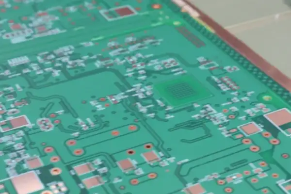
Recently I ran through several suppliers of high-layer-count boards precisely because boards in OTN equipment are getting harder to serve. Many people think redundancy simply means putting more circuits and routing more lines, but what really gives people headaches is the physical implementation of that whole redundancy logic on the PCB. Take the synchronized distribution of the clock unit: it is not the simple star topology mentioned online. If you want the phase not to jump during switchover, trace length must be controlled to a near-obsessive degree, and being off by a few mil can cost you dearly in millisecond-level protection switching. At that time I had a multilayer PCB manufacturer specifically revise one stackup, burying the clock network between two ground layers just to suppress crosstalk, a requirement that many suppliers of ordinary communication boards did not understand at all at first.
The OTN backplane is even more of a bottomless pit. To switch to a backplane with a large cross-connect capacity, the layer count goes directly to above 40 layers, and the stackup is not uniform; there must be a dedicated tension-balancing layer to balance warpage. I tried an ordinary multilayer PCB supplier for the prototype, and after reflow the board bent like a pot lid, and all the connector alignments were off. Later I turned to cooperation with an HDI PCB supplier, because they have muscle memory for high-density buried and blind vias and any-layer interconnect, and I did not need to teach them how to handle the press-fit area of 0.5mm pitch high-speed connectors. Interestingly, some HDI PCB manufacturers actively suggest changing part of the high-speed differential pairs into a hybrid solution of backdrill plus microvia, saying it can reduce insertion loss fluctuation by about 10%, a visible improvement for the analog channel of a coherent module.
What impressed me most was the line board used for running coherent signals above 100G. In the high-frequency area I insisted on using M6-grade material, but the high frequency PCB manufacturer instead went wrong on impedance control, because their reference data was still based on an older resin system. Later I switched to a high frequency PCB supplier specializing in RF backplanes, who directly did differential TDR verification on the test coupon for me and adjusted skew to within 0.2ps. This sounds like nitpicking, but once you have seen the scene where, after room temperature in the equipment room rises, skew drift scatters the constellation diagram, you understand it was all bought with lessons.
The fan speed control circuit in the redundancy structure also cost me a lot of effort. If the PWM signal on a multilayer board is not shielded, its edge noise can couple directly into the analog front end of the optical monitoring channel, causing low-frequency drift of OCM readings. Later I concentrated the speed-control MOSFETs and current sense resistors in a small area of 3 ounce copper, laid a full layer of copper beneath for heat dissipation, and ran a ground line ring around the PWM routing, and it finally settled. These details are not ones the multilayer PCB manufacturer will proactively think of for you; they think passing the electrical rule check is the end of it. But analog circuits and strong digital power coexist on an OTN PCB, and if you do not watch closely yourself, what returns is a pile of boards that cannot pass EMI.
By the way, when selecting suppliers, what I value most is actually not whether the certifications are complete but whether their engineering department has experience with large backdrilled boards. If the residual stub of an OTN backplane is too long, the eye of an NRZ signal above 25G is directly closed by half, which cannot be saved by adding emphasis. Some vendors claim to be HDI experts but cannot even guarantee the accuracy of controlled-depth backdrilling, and their scrap rate is extremely high. Later I settled on an HDI PCB manufacturer willing to drill backdrill test points on every board. Although the unit price is 15% higher, at least there are no batch signal failures, and the account works out. In the end, the redundant telecom-grade architecture of OTN pushes board-level reliability to the extreme, and if a PCB vendor designs only to ordinary industrial standards, tuition is bound to be paid.
I have worked on this type of circuit for some years and dealt with several multilayer PCB manufacturers before. Frankly, the several analog differential channels of an OTN system are far harder to handle than the digital part, by more than a bit. Many people start by staring at length matching, thinking that if the four groups of traces XI, XQ, YI and YQ are pulled to the same length the problem is solved. But engineers who have run modulation above 16-QAM will tell you that length matching is just the entry ticket; what is really deadly is the consistency of loss.
This is not some mystical theory. In an ordinary PCB design, if you add a little serpentine section, you may add a bit of delay, and with some attention to timing, digital signals can still be recovered. But these several channels on an OTN PCB are different: they are coherent, so not only must amplitude be right, the phase relationship must also be locked down. If you wind one line around to match lengths, the dielectric loss and conductor loss brought by those extra few millimeters immediately break the amplitude balance between channels. At the receiving end, once the loss difference among the four components exceeds a certain threshold, it is even more troublesome than the phase deviation caused by length mismatch, and the constellation points simply scatter. I tried deliberately relaxing the loss symmetry requirement for one pair on a receiver card I built, and EVM deteriorated at an astonishing speed.
So now when I look for an HDI PCB supplier, I negotiate loss consistency as the first indicator, followed by impedance and crosstalk. Some multilayer PCB suppliers will pat their chests and tell you they can do 100 ohm differential, 3 percent tolerance, return loss below minus fifteen across the whole band, and of course those matter. But if you stay only at the nominal values on the spec sheet, once the actual board comes back and you measure it, a loss slope difference of a few tenths of a dB between channels is too late to cry about.
I appreciate some high frequency PCB manufacturers who bring glass cloth orientation and resin content consistency into the scope of process control. That is far more meaningful than simply changing to a low-loss base material. Because for high-speed signals on an OTN PCB, what finally limits you is often not the absolute loss value of one channel but the relative deviation among the four channels. Some HDI PCB manufacturers use improved stackup technology and laser drilling that can better ensure consistency of via residual stubs, which is smarter than relying on serpentine routing to chase equal lengths. After all, each additional via adds one more discontinuity, and if you get the topological symmetry of the fan-out region right, you do not need to labor over compensation later.
At the end of the day, the design logic of an optical transport network PCB differs from that of an ordinary high-speed digital board. It forces you to pay attention to details that normally are not noticeable, such as differences in copper foil surface roughness between batches, or whether the reference plane of an inner-layer trace has been broken by slots of other signals. Whenever I think back to the first time I did this project, when a high frequency PCB supplier asked me whether I wanted to control the window effect of glass cloth weave, I thought they were making a fuss over nothing; now looking back, these are the things that truly open the gap. Once the flatness and consistency of channel loss are really solved, many timing and eye diagram problems become less sharp.
Some time ago I chatted with a friend who builds coherent optical modules about the 100Gbaud system board he was wrestling with. The board alone had been prototyped six or seven times, either with impedance off or with return loss stuck at -12dB and refusing to go higher. In the end he took the board to our lab and measured it on a network analyzer, and only then found that the problem was in the via stubs. The first multilayer PCB supplier they found had not backdrilled after lamination and left stubs of almost 12 mil, which at 50GHz behave like antennas and directly eat a large chunk of signal. I measured it, and the resonance notch produced by that stub alone fell exactly in the middle of the band they wanted to use, so it was impossible to use.
In fact, when you play with digital signals above 50GHz, the capability threshold of the board factory is exposed at once. Many HDI manufacturers can get by below 20GHz by stacking layers and shrinking line width, but at millimeter-wave frequencies, a small change in line width or a few microns of dielectric thickness difference can throw characteristic impedance off by two or three ohms. Earlier, when we were tuning a single-ended 50 ohm line on an Optical Transport Network PCB, simulation gave a line width of 4.1 mil, but the first batch of boards measured 45 ohms. After a long investigation we found that the copper layer had been side-etched by nearly 0.3 mil, leaving the actual line width too narrow. Later we switched to an HDI PCB supplier who could control etched shape at high frequency, added etch compensation to 1.25 times the design line width, and the second version stabilized within plus or minus 2%.
About stubs: I now have just one requirement for multilayer board manufacturers. For any channel with a nominal frequency above 40GHz, use laser blind vias all the way through, or backdrill so that residual stub does not exceed 3 mil, and preferably use buried vias to eliminate them directly. The wavelength at 50GHz in the dielectric is only a little over two millimeters, and a stub of such a small length can pull the return loss of a differential pair from -18dB to around -10dB through its inductive reactance, closing the eye completely. Once we received a batch of boards in which, in two halves of the same lamination batch, one side was backdrilled perfectly clean and the other left a 5 mil burr, and the corresponding channels differed in bit error rate by three orders of magnitude. Later I was forced to add a requirement to the acceptance conditions for cross-section sampling of every via. Although the supplier complained that it was too harsh, an OTN PCB is exactly this kind of thing: you cannot negotiate with a signal.
Sudden line width changes are also a big pit. Many people doing RF PCBs are used to gradual transitions, but on high-speed differential traces, every line width jump in the 50GHz band can bring a reflection point. My layout principle now is to keep coupling spacing between differential pair members within 0.8 times line width, so the electric field is locked tighter and the pair resists external crosstalk better. And isolation between adjacent channels cannot be achieved only by enlarging spacing; I generally place a continuous ground via wall between transmit and receive differential pairs, connecting top ground and inner ground densely with vias to form a quasi-coaxial shielding structure, so that near-end crosstalk can be suppressed below -45dB. Realizing such structures well still depends on the laser drilling accuracy and alignment capability of the HDI PCB manufacturer; ordinary mechanical drilling simply cannot make such a dense grid.
Let me say a bit more about material. For a coherent OTN PCB above 50GHz, we basically no longer dare to use FR-4 hybrid lamination, not because of cost but because the batch consistency of Dk and Df is too poor. Earlier, to save a little money, we used FR-4 for the lower half of the stackup and placed high-frequency material only on the top layer and the sub-outer layer. As a result, in a humid environment the phase stability of the whole board collapsed. Later we honestly used low-Dk glass cloth base boards of M6 grade or above on all layers. Although it costs nearly double per square meter, at least we do not have to worry every day about the eye collapsing after temperature cycling tests. So when looking for high frequency PCB manufacturers and suppliers, I pay particular attention to whether they can provide measured Dk data from the same batch, not just the manufacturer’s typical values. Only manufacturers willing to roll up their sleeves on through-hole stub control, copper foil roughness testing and stable line width CPK dare I entrust with a 50GHz design.
When I worked on a coherent optical module for an equipment vendor in the past, my superstition about board material was completely shattered. At that time I always felt that as long as I picked high-end Rogers material with low and stable Dk, the signal quality of the board would be eighty or ninety percent assured. The first batch of prototypes came back with an eye as closed as if it had not woken up. After checking around, I found the problem was the copper foil. Although the board factory used the high-frequency material I specified, the copper foil was ordinary reverse-treated foil with excessive roughness, which raised the conductor loss of the surface traces by nearly double. This might still be tolerable for NRZ signals above 25G, but for the OTN coherent interface, which is extremely sensitive to phase noise, it was simply suicide. Later I switched to a true high frequency PCB manufacturer, who directly used an HVLP scheme with carrier copper foil, and the bond between laser blind vias and copper foil was also cleanly handled, with no more copper peel-off trouble, and the signal finally met the requirements.
This made me realize that a so-called high-frequency material solution is not a matter of buying a few low-Dk cores and pressing them onto FR-4. The difficulty of an OTN board is that the same board has to carry coherent analog signals above 80GHz, plus many 56G/112G PAM4 high-speed digital lines, while power layers must carry tens of amps, and heat dissipation, impedance and interlayer reliability are all mixed together. I once worked with a multilayer PCB manufacturer who, to save money, pushed hybrid lamination hard, mixing Rogers 4350B with Megtron 6. In design, Dk and CTE appeared to match nicely, but after less than two hundred hours of temperature cycling in a small batch, cracks began near the buried vias. Cross-sectioning showed that the two materials had twisted and broken the via wall copper during Z-axis expansion. Only later did I understand that merely looking at the CTE data supplied by the vendor is useless; after actual lamination, glass fiber direction and resin flow concentrate stress at completely unforeseen positions.
Since then I have added another trick to my screening of multilayer board suppliers. I generally do not talk price first and instead ask directly how many layers the most complex Optical Transport Network PCB they have mass-produced had, and whether they have done backdrill plus embedded copper block hybrid lamination, and you know their true level right away. Most of the so-called HDI PCB manufacturers stammer immediately upon hearing about three layers of stepped buried vias plus local copper block sintering copper paste for heat dissipation. A truly experienced HDI PCB supplier who has taken this type of order will discuss with you whether the copper block is formed by etching or CNC routing, and how to ensure step flatness after the copper foil above the block is removed. Such things cannot be summarized without having produced hundreds of square meters.
Another easily neglected point is the frequency-dependent dielectric behavior of copper foil and prepreg in hybrid lamination structures. The Dk value given by the high-frequency material supplier is measured at a single frequency of 10GHz, but the bandwidth of high-speed signals in OTN easily stretches to 30 to 40GHz, at which many materials already have lower Dk, and different materials fall at different slopes. If the board factory calculates impedance with only the nominal value from the supplier, the actual impedance of the finished differential line at the Nyquist frequency can be off by five or six ohms, and if the eye will not open you cannot blame the chip. A truly knowledgeable multilayer PCB supplier will make VNA test boards in the engineering phase, invert the real Dk-Df curve, and use that data to fine-tune line width. Small factories simply cannot afford to cultivate this capability; only factories that have long made optical transport backplanes and line cards accumulate it.
Today when I select an OTN PCB supplier, I treat them as half an RF partner rather than a simple processor. After all, for this kind of board, from embedded copper, laser blind vias and four-sided gold-plated fingers to large-area selective hard gold plating resistant to salt spray, every step may eat up the design margin that came before. For a supplier that can still preserve more than 3dB of coherent-port high-speed signal margin through to mass production, I accept a slightly higher price, because the accumulated knowledge in copper foil, lamination equipment and engineering team heads is worth far more than the laminate model on a bill of materials.
Some time ago I evaluated the hardware scheme of an OTN board for a company making optical transport equipment, and during that period I was ground down by all kinds of problems until I had no temper left. Many people who discuss OTN keep their eyes only on the protocol layer and coding gain, as if choosing a strong enough FEC algorithm would let the link budget rest easy. But once the board came back and the eye diagram jittered like an electrocardiogram, you realized that what truly chokes the throat is often in unremarkable places of the physical layer.
I have dealt with several factories that labeled themselves multilayer PCB manufacturers, and some even said they could make high-frequency PCBs, but the OTN PCB samples I received showed a mess of microstrip impedance consistency on the surface layer. On OTN logical interfaces that routinely run tens of Gbps, the hard-core FEC encode and decode module has to be tangled with hundreds or thousands of high-speed SerDes traces, and if reflection and crosstalk go slightly out of control, FEC’s correction capability is directly discounted. This is not a problem with the algorithm itself; the execution environment is simply too dirty. You spend all your effort tuning RS-FEC, and then, because the stub of one or two vias was not backdrilled clean, the equivalent eye opening at the receiver drops by more than ten millivolts and the bit error rate floats to the sky.
That experience made me recognize a reality: finding the right multilayer PCB supplier matters far more than agonizing over coding parameters. The stackup design of some vendors simply cannot handle the layer count needed by 100G OTN boards. Later we turned to cooperation with a team that specializes in HDI PCB, whose HDI PCB manufacturer process is much finer in laser drilling and microvia copper filling, and after routing density went up, the delay difference between the FEC module and the switch chip actually went down. It is quite interesting to say: after signal integrity at high speed improved, an old-model FEC chip actually achieved a lower post-FEC bit error rate than the newer chip before it.
Another trap that is easy to step into is how byte interleaving of FEC subframes lands at board level. The protocol is written very cleanly: each row generates 16 FEC subframes with byte interleaving and de-interleaving. But on the board you must deal with the source-synchronous interface between the FPGA and the dedicated FEC, and if routing is slightly uneven, the buffers of the interleaver and de-interleaver overflow easily, and that kind of intermittent block loss is the hardest to find. We once got stuck for more than two months, and in the end found that the pin-field escape scheme supplied by an HDI PCB supplier had introduced a tiny timing skew that, accumulated, crashed FEC’s hard decision module exactly at certain temperature points. You see, this is the gap between theoretical correction capability and real hardware.
So now, when someone asks me how to optimize an OTN link, I no longer pull out the generic routine of tuning equalization first and then changing FEC. I prefer to ask: who made your board? What laminate did you use? How much backdrill tolerance did you leave? If the multilayer PCB manufacturer only dares to be sloppy on the through holes, then even the stronger OFEC burns power in vain. Only teams that have grappled hard with board material loss and machining accuracy can make those densely packed FEC check bytes truly useful. Moreover, for an Optical Transport Network PCB used in a high-density OTN line card, whether the power and ground planes can be cut cleanly across more than 20 layers often affects whole-board performance more than which specific FEC chip model is chosen. Digital front-end people do not like to talk about these things, but engineers who have run several rounds of hardware iterations all keep this ledger in their hearts.
In my earlier days making OTN equipment, the biggest pit I stepped in was actually neither protocol nor algorithm but the board itself. Many people talk about OTN and steer the topic toward FEC and DSP, believing that as long as the chip is chosen correctly, the bit error rate will naturally drop. But I found that if the Optical Transport Network PCB underneath is not built solidly, no good algorithm running on it matters. The DSP in the chip does soft decision, and FEC corrects errors with all its might, but once the signal leaves the chip, runs several inches of trace to the backplane connector, and the eye has collapsed beyond recognition, the correction capability is only good for filling pits.
Now, when making a high-speed board, especially in an OTN scenario where single lanes easily run at 28G or 56G, finding the right multilayer board manufacturer is far more realistic than agonizing over an LDO. I used to cooperate with quite a few multilayer board suppliers; some give you ordinary FR-4 whose inconsistent thermal expansion coefficient makes the board slightly warp after reflow, and the impedance of high-speed differential pairs drifts away. Later I changed to one specializing in high-frequency boards, using M6-grade or above base material. Cost went up, but at least I do not worry all day about the influence of via stubs on 56G signals. Many people ask me why I am so picky about multilayer board manufacturers, and the reason is simple: when you see a 25Gbps signal eye open cleanly at the receiver, that sense of security is not something you can get by tuning a few lines of FEC parameters.
Another often neglected point is the abuse of the HDI process. Not every high-speed region is suitable for HDI stacking. Some HDI PCB manufacturers, to show off their capability, immediately recommend third-order and fourth-order stacked vias, wishing to use microblind vias on the whole board. But OTN boards are often not small, with slot widths of a standard chassis, and doing high-density interconnect on such a large board, a slight layer misalignment brings out differential skew. Later I learned my lesson: I use first-order HDI only in the BGA breakout area and honestly use through holes elsewhere, requiring the HDI PCB supplier to follow one stackup structure strictly and not change materials on their own initiative. Put plainly, what I need is controllability, not showing off.
The theories of DSP and FEC coordination sound impressive, such as probabilistic constellation shaping approaching the Shannon limit, but once back at board level, it is purely physical constraint. After falling into the pit of line length mismatch on that group of high-speed SerDes between the DSP and the FEC chip, I understood what it means to be driven mad. The DSP at the receiving end sends soft information to the FEC chip, but because one differential pair was 5 mil different in length, the deterministic delay of data transmission changed, and the decoder received misaligned information, and you do not even know how to investigate. This incident made me fully realize: stop staring at the coding gain of the protocol layer, and treat the link from DSP to FEC as RF, which is better than anything else.
Now if you let me choose a cooperating high-frequency PCB manufacturer, I look at just two points: first, whether they have made communication backplanes of the same rate, and second, whether their impedance test reports dare to mark the actual value of every board rather than a design value to muddle through. Many high frequency PCB suppliers have beautiful samples with flat solder mask, but once in small-batch consistency they are exposed. I have suffered here: after soldering several hundred boards I found that a batch had differential impedance dropped by several ohms, and the whole batch was scrapped. At such moments who has the mood to talk about the OTN frame structure or parity byte overhead; it is all tears. So I would now rather spend more budget on this step and find a reliable multilayer board PCB maker to stabilize the supply chain end, then tune the FEC parameters afterward, which is truly icing on the cake.
A few years ago I took part in an OTN transmission equipment project, and at that time what gave me the biggest headache was not the system architecture but the selection of the circuit board. Many people think OTN is just plugging in a few boards and configuring some optical modules, but when you really do it, what holds up progress is often invisible basic material, especially the PCB carrying high-speed signals. We dealt with several multilayer board vendors at the time and found that many manufacturers claiming to make high-end communication boards could not control loss once they ran into 56Gbps or even 112Gbps SerDes routing. Later I slowly came to understand that an Optical Transport Network PCB cannot be treated as an ordinary digital board; it is more like handling weak analog signals and high-power digital circuits on one board at once.
During that stage we tried many suppliers. One quite famous HDI PCB manufacturer indeed had good laser drilling and could make very dense vias in local areas of the board, but its material library did not fully support low-loss laminates. The traces between the optical module and the DSP on an OTN board require extremely low insertion loss, and sometimes a single differential line runs more than ten inches, so with ordinary FR-4-grade material the eye collapses outright. So later we had to reevaluate the supply chain and turn our eyes to high Frequency PCB manufacturers who truly have accumulated experience in communication backplanes. The difference in high-frequency board experience showed at this point: people who know the business will suggest a specific copper clad laminate model and even fine-tune the stackup to balance impedance and glass weave effect, instead of drawing it for you off a template.
But the problem came again: many high-frequency board factories are good at small-size microwave module boards, and when they meet large-size OTN backplanes of dozens of layers, process stability fails again. Boards in OTN equipment are often hybrid structures with a power section of over a hundred watts and dozens of high-speed interfaces, and the thick heat-dissipating copper is such that even one reflow requires a specially tuned profile. This is where you need a multilayer PCB supplier who does not merely handle lamination layer counts but can define the process boundaries with you. The one we later cooperated with made locally dense routing into HDI in the form of a daughter board, then connected the daughter board and the main multilayer board through buried vias, which balanced density without hindering thermal management of the whole board. This hybrid structure saved the signal integrity of the whole project at the time.
Speaking of modules, the pluggable optical modules used in OTN systems already have considerable power consumption, and the board also has to hold various power management units supporting hot-plugging. If board-level layout is slightly unreasonable, heat gathers under the cage and cannot dissipate. The most outrageous design I have seen had several large-current MOSFETs right under the optical module, and when temperature rose, the module started erroring wildly. This also reminded me that when choosing an HDI PCB supplier you cannot only look at their line width and spacing capability; you must also ask whether they have done similar high-power and high-speed mixed designs. Some suppliers are very honest and will tell you directly what temperature continuous loading will reach under such a stackup, rather than muddling you with simulation data.
Looking back now, OTN system-level products depend on PCBs far more deeply than imagined. The board carries not only the logic links but also the heat dissipation path and power redundancy of the whole equipment. More and more high-speed signals run down from the backplane, forcing you to re-understand materials, vias and stackups. In future, when choosing a supplier for an OTN PCB, I will certainly first have them measure the inner-layer alignment and signal loss of a hybrid-lamination structure on several large multilayer boards, rather than looking only at qualification documents. A truly reliable multilayer PCB manufacturer does not brag about parameters on a quotation but tells you the stress boundaries of the board ahead of time. Some pits are better stepped in early, and one feels more settled for it.
A few years ago I designed a board card for a metro WDM equipment, and I was truly tormented by the Optical Transport Network PCB. Many people think OTN PCB is merely about pulling through high-speed serial links, but once you actually run it, you find that just keeping dozens of 25G signals obediently within the eye mask takes a long fight over stackup and vias. At that time I contacted many multilayer PCB manufacturers and finally settled on a multilayer PCB supplier with fairly reliable delivery. It was not because the price was so good but because they dared to commit to holding the alignment accuracy between two layers within 50 microns. This is critical for clock distribution on the backplane; being off a little would make phase jitter during master-standby clock switchover impossible to suppress.
The fan matter is also interesting. We originally thought zoned fan speed control would save a lot of power, but when I actually drew the board I found that temperature sensors cannot be stuffed in arbitrarily; they must be placed right against the switching chip and the retimer, and the I2C traces must not run parallel to the PWM control lines, otherwise the temperature values read out jump around, and the fans scream one moment and stop the next. During the two weeks of debugging, the equipment room was full of the echo of us cursing. Later I simply separated the fan control unit onto a small daughter card isolated from the high-speed area, and directly found an HDI PCB manufacturer to prototype that control daughter card, because the component density was too high and an ordinary through-hole board simply could not lay out those current-sense amplifiers and bypass capacitors. This also forced me to re-examine the selection criteria for HDI PCB suppliers. Previously I only looked at line width and spacing, but later I found that the taper of laser drilling and the uniformity of copper filling have a great influence on the analog sampling accuracy of the fan control circuit.
The PSU part is something many people consider a power engineer’s matter that has nothing to do with signal integrity. But an OTN chassis easily holds a dozen PSUs, and when they sleep under light load, half must be shut down, and the switching noise of those power MOSFETs couples along the backplane into the clock recovery circuit of the adjacent slot. I suffered once: during a certain stress test, at the instant a sleeping PSU was woken up, the phase-locked loop of the active cross-connect chip lost lock, and service was interrupted for 20 seconds. Later we mandated that the enable control lines of all PSUs must have isolation, and the ground plane partitioning of every board must be coordinated with the return path design of the whole machine. This made me realize that choosing a high frequency PCB manufacturer cannot only look at how many G of signal they can run; you must also ask whether they have done complete power-ground simulation, especially where multiple groups of power planes and ground layers alternate in a multilayer board, where the resonance points lie, otherwise the bottom line of clock phase noise cannot be kept.
On the cross-connect redundancy, we did not take the old path of 1+1 hot standby but tried load sharing. The active and standby cross-connect chips process data at the same time, and output enable relies on hardware arbitration. It sounds perfect, but if the power ripple of two cross-connect chips is not synchronized, periodic deterministic jitter is generated. Later we had a high frequency PCB supplier specially make the two core power planes mirror-symmetric in the stackup, with the length difference controlled within 0.5 millimeters, which pressed the problem down. Likewise for clock unit master-standby switching: many people think software switching is enough, but microsecond-level holdover simply cannot rely on algorithmic compensation, and it all depends on the low-noise PLL and clean reference source on the board. So each time I chat with manufacturers, I ask how far they take copper guarding and ground wrapping on clock traces, and this detail is more truthful than any parameter.
All in all, after several OTN projects, I feel that what is hardest is not some single-point technology but coordinating seemingly independent functions like fan control, PSU management and clock redundancy within dozens of layers of board; if the ground bounce or crosstalk is not handled in any one place, packets will be lost on the optical port in the end. So now when someone asks me to recommend a multilayer PCB supplier or an HDI PCB supplier, I prefer to talk about whether they have whole-backplane SI/PI co-simulation capability rather than simply compare layer count and minimum line width; that is what can truly save you from cabinet flashing in the middle of the night.
After so many years of making OTN equipment, my deepest understanding is that if the board’s materials and process are chosen wrongly, however beautifully the algorithm is tuned afterward, it is useless. Many people start by discussing FEC gain and modulation formats, but if the underlying PCB is not figured out, those indicators look good only in a laboratory thermostat, and in the field they immediately show their true colors.
The several 800G coherent interface projects I handled all stumbled in the same place at first: relying too heavily on upstream reference designs, assuming that placing orders according to the original manufacturer’s recommended stackup and materials would do. As a result, when the first batch of Optical Transport Network PCBs came back and was plugged into an optical module for a stress test, the eye was smeared outright and EVM drifted beyond viewing. Later I sent the board for cross-section analysis and found that the supplier had on their own initiative replaced the prepreg with one of much higher loss, with the excuse that you did not specify a brand. Since then I no longer leave the choice of multilayer board supplier to purchasing. To choose a multilayer PCB manufacturer, you have to go and look at their high-frequency material inventory yourself, check whether they have truly done projects with bandwidth above 60GHz, and not listen to sales patting their chests.
Some people think HDI can solve all signal integrity worries, but my experience is just the opposite. There is one case where I insist on traditional multilayer boards: when your board is large and has a lot of optical module cages that need structural support. In terms of Z-axis expansion coefficient, multilayer boards actually behave more controllably than some HDI stacks, especially in hybrid lamination of high-frequency material and ordinary FR-4. A multilayer PCB supplier I cooperated with had a lamination process that could control CTE mismatch within a very narrow range. Their method was very simple: pre-shrink the cores of different materials before lamination. This detail is not done by many HDI factories, because they assume you are using the same type of board material throughout. The HDI PCB supplier I used, by contrast, let me down on this point.
Speaking of high-frequency materials, selecting a high Frequency PCB manufacturer is unavoidable. There is a great deal of material with nominal Dk below 3.5 on the market, but few can truly keep a 56GBaud signal running steadily on an OTN PCB. My own habit is that, for each new supplier, I first have them make a batch of impedance strips and microstrip resonant rings with the same stackup, and then I measure them myself on a vector network analyzer up to 110GHz. Do not trust the vendor datasheet; those data were measured with standard copper foil and standard lamination conditions, which is a hundred thousand miles from your actual process conditions. I encountered a high Frequency PCB supplier that used the same Panasonic M6 material, yet the board’s insertion loss at 30GHz was nearly 1dB higher than another’s, just because the copper foil roughness and the brown oxide process differed. So now when selecting suppliers, I always require them to attach impedance test reports under actual process conditions with the board, not simulated values.
I also took a detour regarding layout near the FEC chip. In the past I regarded OFEC as a purely digital circuit and treated it only by the rules of a high-speed digital board, with the power rail using an ordinary LDO plus a few decoupling capacitors. Later I found that decoding and error-correction performance occasionally jumped, and after a long time of investigation I located it to the transient current of the DSP on the board crosstalking through the shared power return to the PLL of the FEC chip. The solution was instead of changing to some expensive PCB material, to make a tiny power island on the OTN PCB, use a dedicated ultra-low-noise LDO to power the FEC PLL, and connect the copper of this area directly to a complete ground plane layer with no vias in between for transition. I rarely see this handling on boards made by peers, who often put all their effort on laser driver and modulator bias circuits and think the FEC can be placed casually.
When selecting an HDI PCB manufacturer, I particularly value their ability to handle backdrill stubs. For the differential pairs running above 28Gbps on an OTN board, a stub of seven or eight mil can ruin both insertion loss and return loss. But the reality is that many HDI factories write in their marketing materials that they can control to within 6 mil, yet the stub length dispersion in actual batch production is shockingly large. The HDI PCB supplier I later settled on for long-term cooperation uses depth-set camera automatic inspection and photographs and archives the backdrilled holes of every board. The cost is higher, but it saved me a great deal of debugging time. This kind of hidden cost is never reflected when computing the BOM.
In past projects, I stared at several boards scrapped due to overheating and thought about a question: we put too much effort into redundancy at the system and equipment level, but rarely look down at the OTN PCB itself that carries all the signals. Once a shared critical node exists on the board, the 1+1 protection written in the scheme is as fragile as paper in the face of reality.
When looking for a reliable HDI PCB manufacturer or multilayer PCB manufacturer, you cannot look only at whether it can route the lines. During lamination of a high-layer-count board, if the interlayer alignment deviation reaches a few mil, your 100 ohm differential pair goes off directly, and the signal margin eaten by impedance degradation cannot be compensated even by the back-end FEC. I have seen some boards where, by design, the FEC overhead area and the service-mapping channel physically shared the same power filter network. As a result, the instantaneous current fluctuation of the FEC chip crosstalked directly into the service-side DSP. Such common-cause failure makes redundancy meaningless, because you cannot even cut off the fault point; the source has already seeped in.
Many people think an OTN PCB carries digital signals and is therefore strongly immune to interference. But anyone who has done it knows that the XI/XQ channels coming from a coherent DSP are essentially handling analog signals degraded by long-haul transmission, and if board-level loss differs by even 0.5dB, or the backdrill stub is a few tens of microns longer, the Q factor can be pulled down a step. At that point, how can the so-called redundancy cope? If the primary and standby links run over the same region of base glass cloth with severe weave segregation, or the reference ground return shares a stretch of highly inductive copper, then the thermal redundancy path of this board is fake. At high temperature, the different expansion coefficients of the dielectric glass fiber direction make impedance drift take both primary and standby channels down together.
Truly reliable high-reliability boards, whether you look for an ordinary multilayer PCB supplier or a specialized high frequency PCB manufacturer, all depend on whether they carve independence into their bones. Power redundancy is not done by adding an OR-ing circuit; rather, each PSU’s input, filtering and reverse protection all the way to the chip pin must have copper width, via count and fuse isolation planned separately. I met a high-frequency supplier who, when making backplane clock redundancy, deliberately pulled the two groups of traces from the sending end of the primary and standby clocks to the receiving chip more than 10 millimeters apart, stuffed the space between them with grounding shield vias, and calculated even edge coupling to the end. When such a board came back and was tested, with the primary clock path interfered with, the jitter of the standby path hardly moved. That is what on-board redundancy should look like: physically cut cleanly, so that software can play with switching.
Another easily neglected point is the fit between the board and the subrack airflow. If, during design, your Optical Transport Network PCB places high-power FEC chips and DSPs in a recirculation dead corner of the air duct, then a local ambient temperature rise exceeding 25 degrees can turn what is in theory 100% protection switching into a situation in practice where the protection board overheats before the working board. A good layout always determines device positions from the thermal perspective first, and routes high-speed lines afterward. HDI PCB suppliers with their own thermal simulation teams will give you a detailed power density map telling you that copper thickness here must be 3oz and a thermal via array should be placed there. Redundancy is not only logical redundancy of adding one more board but also the requirement that the heat dissipation path of every watt on the baseboard has a backup.
At the end of the day, redundancy on a board is a systems engineering matter, extending from component selection and dielectric Dk stability to stackup symmetry design and routing physical isolation, and slacking off at any place ultimately becomes a case of protection failure. The next time you hear someone say this board has 1+1 redundancy, you might ask: are your LDOs two independent ones? Do your clock buffers share? How much does the thermal gradient of your board differ between primary and standby areas? If you cannot answer these, then the so-called redundancy is just two lines of copper running side by side physically, and when disaster comes, nobody can save you.
After nearly ten years in hardware and dealing with all kinds of board factories, my deepest feeling is that between a technical parameter saying can satisfy and actual mass production without strange troubles lies the reliability of an entire supply chain. Last year we had an optical transport project with 56Gbps PAM4 on the board, a DSP plus a pile of optical modules, and a frighteningly high power density. During the design review everyone stared at the simulated eye diagram over and over, but the problem finally came out in the material hybrid-lamination part. The high-speed layers used low-loss board material, and the power and low-speed signal layers used ordinary FR-4. The board factory did not control CTE matching well during lamination, and under temperature cycling, microcracks appeared directly in the inner-layer copper, the signal broke off from time to time, and it was killing to investigate.
This incident made me rethink a simple truth: choosing a multilayer board manufacturer cannot look only at how many layers they can make and how fine the line width and spacing are; you must look at whether they have real volume production experience with mixed stackups. Some HDI board factories can make the fine buried holes of phone motherboards, but when they meet large-size high-layer-count boards, resin flowability and interlayer registration are exposed. And traditional multilayer board suppliers may be very stable at making backplanes, but when it comes to HDI structures requiring any-layer interconnect, laser drilling quality and copper filling capability are a notch short. Our OTN board card happened to have both ends: high-density BGA areas needing HDI process and dozens of layers of high-current power layers. So finding the right supplier was more critical than choosing the board material model.
About hybrid lamination, I am not a materials expert, but from stepping in pits I have gained some wild-path insight. You cannot look only at the nominal values of Dk and Df; you must also care whether the flow windows of the two board materials during lamination are close, otherwise a hidden illness appears in interlayer bonding. Once, when we prototyped, the board factory used a high-frequency board material hybrid-laminated with FR-4, and the stackup report they gave clearly said it matched. The board came back for a thermal stress test, and the inner layers delaminated. Later it was found that the two materials had too large a Tg difference, plus their lamination program had not been optimized for this combination. Later I changed to an HDI factory that had done the same kind of hybrid combination, and with the same design files, this problem did not occur again. So reliability cannot truly be calculated on paper; it is tested out on the factory production line, furnace by furnace.
Hardware engineers are often led by high-speed signal integrity, spending a lot of time adjusting length matching and calculating loss. But I increasingly feel that without a solid heat dissipation path and robust power distribution, even the most beautiful eye diagram will be ruined once on the rack. On that OTN single board of ours, we densely drilled thermal conduction holes under the optical modules, made copper thickness 2oz, and also used embedded copper blocks to assist heat transfer. This set of processes looks simple but is actually a test of the HDI manufacturer’s layer registration and post-lamination flatness. One supplier made a board in which X-ray showed fine resin voids around the embedded copper block, and the thermal resistance of the heat dissipation path was higher than the design value, and the optical module temperature spiked by more than ten degrees. Later we moved the order to a factory specializing in hybrid lamination of high-frequency and HDI, and with the same embedded copper block structure, their resin filling process was well controlled; the TEM cross-section looked very clean at the interface, and the measured junction temperature returned to normal. So do not take manufacturing capability lightly; however perfect the designer’s intent, only on the production line does it show its true character.
This also made me realize that when selecting suppliers, you cannot look only at the words high frequency PCB manufacturer or HDI PCB supplier on a website; you have to go and see on site whether their solder mask exposure machine has fine bridge compensation, whether the plasma desmear equipment really runs a pass, and whether they do batch sampling inspection of TDR impedance tests. Now some factories can provide simulation support with built-in copper block thermal models, which has helped us a lot in optical module thermal layout. To be honest, the time spent on supplier audits later came back through less rework in the late stage of projects.
Many people in hardware like to chase the new: ultra-low-loss materials, mSAP processes, substrate-level FC-BGA, all sounding high-end. But when it comes back to volume delivery, honestly smoothing the Dk transitions between stackup layers and raising via reliability is more useful than piling up parameters. An optical transport board runs for five or eight years, and what truly kills it is often not a slight insertion loss difference but the fatigue of some mixed-lamination interface, or a hot spot produced by a thermal via because of uneven copper thickness.
Drawing a 48-lane PCIe Switch PCB sounds like just a more complex
An SD-WAN hardware project showed how complex these boards really are: in
Several fabricators turned down our 38-layer TPU PCB. Splitting it into a
- Expert på produktion av små till medelstora serier
- Kretskortstillverkning med hög precision och automatiserad montering
- Pålitlig partner för OEM/ODM-projekt inom elektronik
Öppettider: (mån-lör) från 9:00 till 18:30
Get quote, solution or any question, Andre always here to help