

Wireless EV Charging PCB: How Heavy Copper, Parasitic Inductance, Gate Loops, and Foreign Object Detection Shape Board Design from 85kHz to 6.78MHz
From 85kHz to 6.78MHz, a wireless EV charging PCB gets far harder:
In a multi-slot PAC, the backplane is the silent spine of the control station: it distributes tens of amps of 5V and 3.3V current, carries the module bus, and has to survive hot-swap surges, vibration and years of thermal cycling. Many unexplained drop-outs, module resets and communication errors trace back to the Programmable Automation Controller PCB rather than to the controller or the program. This article collects field lessons on inner-layer copper weight, base copper versus plated copper, layer registration, Z-axis expansion in thick copper laminates, slot power planning, bus topology (parallel, serial, Ethernet-style), thermal paths and hot-swap soft start. It also explains how to question a heavy copper PCB supplier or a multilayer PCB manufacturer, using cross-section reports and proven industrial backplane history instead of price or layer count. A short FAQ follows at the end.
In the early years, when I was doing equipment control cabinet integration, I stepped into a pit that still hurts to remember. We were retrofitting a production line. The PAC controller itself was a big-name brand with a very stable reputation in the market, and the logic program had been verified over and over, so everyone felt nothing could go wrong. After the equipment ran, stations dropped every few days, and expansion I/O modules would go offline for a few seconds and then recover by themselves. We checked the communication cables, the termination resistors and the grounding, and struggled for two whole days. In the end we took the whole backplane off and sent it to the board factory for cross-section analysis, and what a find: the inner-layer copper thickness was uneven, in places it did not even meet the most basic current-carrying capacity, and a whole ground-return copper trace had micro-cracks from lamination. This backplane PCB was the most silent bone in the whole system. It makes no sound, but once it has a problem, no amount of advanced controller modules plugged into it will help.
People in industrial control who talk about PAC habitually put their energy on visible parameters such as CPU clock speed, scan cycle and redundancy switchover speed. But after dealing with a dozen or so PAC systems of different brands over these years, I increasingly feel that what really decides whether a PAC can run steadily for ten years is that backplane whose shape has almost no presence. Especially when you face a rack-type PAC with multi-slot expansion, the physical bus topology on the backplane, the copper thickness of the power traces and the lamination reliability of the multilayer board cannot be remedied by software at all. You might say that the base board of a programmable automation controller is just a few rows of connectors and a few layers of copper. In fact it is the spine of the whole control station: modules plug into it, data runs through it, and tens of amps of 5V and 3.3V current are also distributed through it. Once the spine develops bone spurs or turns brittle, a clever head is useless.
So later I set myself a particularly stubborn rule: when I get the drawings of any PAC backplane, I do not talk about slot count or which high-speed bus it supports; I first look at copper thickness and layer count. Whether the 3 oz a manufacturer claims is truly 3 oz base copper or a plated-up “equivalent 3 oz” must be asked clearly of the heavy copper PCB supplier. In a large automation line, one backplane may carry a dozen analog modules and motion control modules at once, and the transient current on the 5V bus is far fiercer than the nominal rating; if the copper is 20 microns thinner, local heating is completely different. Not to mention some heavy-duty applications where the backplane directly distributes 24V field power: if such traces use ordinary 1 oz copper, after two or three years the copper foil fatigues in thermal cycling, line resistance drifts up, module supply voltage drifts down, and the fault symptoms become all sorts of strange things that the electrician on site simply cannot locate.
When choosing a multilayer backplane there is another easily neglected blind spot: layer-to-layer registration error. I have personally seen a fourteen-layer backplane in which one inner layer shifted by less than 3 mils during lamination, so the impedance of a whole differential bus drifted over its entire length, and the bit error rate exploded during high-speed serial communication. Only after cross-sectioning did we find that the multilayer pcb manufacturer, to meet the delivery date, had simplified the positioning step for inner-layer punching. A board like this passes the continuity test one hundred percent and looks perfectly intact, but the moment a signal of several hundred megahertz runs on it, it starts to haunt you. The PCI Express or high-speed serial backplane bus running on a PAC backplane is actually very demanding on the eye diagram, and if the board factory has not made special compensation in the lamination process for thick copper and multilayer structures, measuring static continuity of the finished board in the lab is meaningless.
There is also the matter of thermal structure. Most hardware engineers focus on the gaps between modules and the fan air duct design, but rarely think that the copper foil distribution of the backplane itself is a passive heat-spreading plane. On a high-current heavy copper PCB backplane, making the power layer and ground layer thick enough and wide enough is not only to lower resistance but also to cool the modules plugged into the backplane from below. We once compared two PAC backplanes with the same slot count specification: one used an ordinary multilayer board process, and the other used a heavy-copper scheme made by a real heavy copper PCB manufacturer. After two hours at full load, looking at the temperature distribution near the slots with a thermal camera, the hottest point of the latter was almost nine degrees lower. What nine degrees means on a semiconductor life curve I do not need to explain.
So whenever a new control cabinet scheme needs my final decision, I always pull the backplane’s multilayer pcb supplier out of the BOM and audit it separately. What I look at is not whether they can make it but whether they have long experience supplying industrial control base boards. Thick copper drilling, desmear, hole-wall copper thickness and flatness after resin plugging are not at all the same difficulty level as for an ordinary multilayer board.
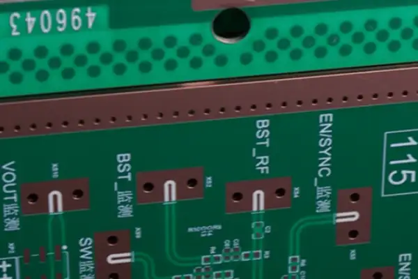
After so many years in industrial control integration, I increasingly feel that the most underestimated item in a PAC system is that backplane. Most people stare at the CPU scan cycle and the module channel count, but however lively the bus runs, in the end everything has to pass through the traces on the backplane PCB. Some abnormal crashes and inexplicable module dropouts on site, traced to the end, are often not protocol problems but tiny deformations of the multilayer board under temperature and vibration that shifted the impedance of the differential pairs.
This is especially obvious in heavy-duty settings. For example, in a steel mill or underground belt control, the inrush current at the moment of module hot-swap can make the copper foil temperature rise sharply. Without a thick copper process, an ordinary board below 3 oz cannot survive many insertion cycles before the edges of the copper bubble and delaminate. I paid for this early on: to save trouble I picked a multilayer pcb manufacturer with a low quote, but they had never handled industrial-grade thick copper lamination, and copper cracks inside the vias disturbed the current distribution of the entire backplane until the whole rack collapsed. Since then I have remembered firmly that I must find a heavy copper pcb supplier with real experience; being able to print a board is not the same as being able to do industrial control. A qualified heavy copper pcb manufacturer will consider the match between copper thickness and the prepreg between layers, and can even calculate the coefficient of thermal expansion for you, which is what guarantees the current-carrying capacity and mechanical life of the power bus on the backplane.
The mechanical stress of a modular structure then tests the interlayer bonding strength of the multilayer board. Many PAC PCBs are 8 or even 12 layers, running high-speed differential buses and tens of amps of power at the same time, with the ground layers also having to share the cooling duty. Without a solid multilayer pcb supplier, if the lamination deviation is just slightly larger, then once the few mounting screws are tightened the board develops micro-strain, and after some time certain through-hole pads fracture. I have seen a backplane where the oblique force of module insertion alone tore a crack several millimeters long in a split ground layer inside, leaving the reference plane of a local bus floating. It sounds mysterious, but on a site with strong vibration, this kind of physical failure is harder to troubleshoot than electrical problems.
More and more controllers now turn the backplane bus into an Ethernet-style expansion architecture, in which the physical distance between modules can stretch to hundreds of meters. This seems to ease the burden on the backplane, but it actually demands more precision in board-level power management and clock distribution. Because each expansion backplane is in essence a local Programmable Automation Controller PCB subsystem, it still needs a stable power network and a low-jitter reference clock. In such cases, the stackup planning of the multilayer board and the attenuation that copper foil roughness imposes on high-frequency signals become a hidden threshold. If it goes wrong, check-retransmissions on the bus become frequent and the processing cycle is falsely inflated; it looks as if it is working, but efficiency has actually dropped a great deal.
So when I organize project specifications now, I never treat the backplane as just a “passive connector”; it is itself the skeleton of the system. When choosing a supplier, I always go over copper thickness, layer count, dielectric thickness tolerance and wear resistance of the surface finish face to face with their engineers. Besides, the upgrade cycle of a modular PAC system is often longer than that of the whole machine, and a backplane with enough design margin can span two or three generations of I/O module replacement, saving far more retrofit money than the small purchase price difference saved by cutting cost at the time. Anyone who has run a few sites can work out this account.
Working on PAC controller hardware, I have never considered the backplane a simple adapter board; it basically decides the expansion capability of the whole system and how reliable its signals are. Years ago I took apart a GE RX3i rack, whose PCI backplane and the traditional 90-30 serial backplane share one connector, which physically forces you, when making a Programmable Automation Controller PCB, to plan the pin partitions very clearly, otherwise plugging in a wrong-generation module either burns the interface or drags the bus levels down. Later, when I drew a PAC PCB of my own, I went directly to a supplier that could make heavy copper PCB for the backplane section, because the supply traces have to pass more than ten amps of continuous current, and with or without hot-swap, the current-carrying capacity of the copper foil must be considered. A conventional 1 oz board visibly changes color and shows rising voltage drop after a few live insertions. In cooperation, a reliable heavy copper PCB manufacturer will not just pile on copper thickness; it will also remind you of the effect of thick copper on interlayer bonding strength and of the release of thermal stress along the large-current path.
On the bus side, the ideas of different manufacturers actually conflict a lot. An architecture like the Aotuo NA400, which uses a serial backplane, simplifies the number of slot signal lines but places higher demands on protocol processing on the module side, while the Delta AH500 insists on the high-speed throughput of a parallel bus, and behind it the multilayer pcb designer has to fight over length matching and impedance. At this point choosing the right multilayer pcb supplier is critical: some manufacturers control four and six layers very well, but beyond ten layers the layer shift and dielectric thickness tolerance start to drift, and the eye diagram of high-speed differential pairs cannot be looked at. One of our batches of boards ignored the lamination parameters of the multilayer pcb manufacturer at the initial prototyping stage, and as a result the jitter of the PCI clock exceeded the limit and the whole batch was scrapped. Only after paying this tuition did I understand that a multilayer board is not a mere processing step; it is itself part of the physical characteristics of the backplane.
Module compatibility is also an increasingly headache-inducing matter. Modular I/O like the APAX-5000 must not only be powered when plugged into the backplane but also deal with devices of different logic levels and different response speeds. This means your backplane cannot pull just one set of buses; it must be segmented and isolated by functional area, and some low-speed modules simply go through independent serial channels so as not to slow down the arbitration efficiency of the whole PCI bus. Reflected in the PAC PCB, this means making one board into a collection of several “virtual backplanes”, with power, ground, high-speed bus and low-speed scan lines all split apart; otherwise, once there are many modules, interference and reset problems can debug you into doubting life. In the end, whether the backplane form is PCI, serial or mixed bus, what finally holds the bottom line is the board material process and the care in layout, which is why I later put the evaluation of the heavy copper PCB supplier and the multilayer pcb manufacturer at the same priority as chip selection.
After running a few factory projects I finally understood that the hardest part of a PAC system is not the control algorithm but that seemingly dull backplane. Every time I/O has to be thrown out dozens or even hundreds of meters, the backplane immediately changes from a simple circuit board into the ganglion of the whole production line, and once the signal stumbles here, the most powerful controller behind it is useless. I took part in a renovation at a plastic woven bag factory where the original control cabinet space was entirely occupied by new equipment, and the digital modules had to be moved to an auxiliary cabinet at the other end of the workshop, at a distance of nearly eighty meters. During that period I spent almost all my time choosing the backplane scheme and communicating with PCB manufacturers.
At the first prototype I took the easy way and handed the Programmable Automation Controller PCB design straight to a quick-turn factory I often worked with, thinking that drawing a four-layer board following the reference circuit would do. When the board came back and was powered up, the power layer on the backplane simply could not take it. I had forgotten that the dynamic current these modules need was much larger than before, and the copper was made only 1 oz thick, so in less than two weeks faint burn marks appeared on the copper. Later I urgently switched to a factory that had really done work as a heavy copper PCB manufacturer, redid the inner layers with 2 oz thick copper, and also laid generous heat-spreading copper areas near the bus interfaces of the backplane. The engineer told me that a PAC backplane often has to carry module power, and thin copper looks like saving cost but is actually planting a mine for later maintenance. Since then I have formed the habit that before ordering such a PAC PCB, I must first confirm whether the manufacturer has mass-production experience with thick copper backplanes, not just whether they can make multilayer boards.
The multilayer board itself is also a watershed. Whether to use blind vias or back drilling directly affects the signal reflections after expansion. Once, we used an Ethernet backplane for remote expansion, with the racks connected by standard Ethernet cables, and each backplane had to carry its own Ethernet PHY and pulse transformer, so the board instantly went from a simple four layers to six or even eight layers. At that point, choosing a multilayer pcb manufacturer cannot be only about price; you must look at their ability to control the impedance of high-speed differential pairs. The time I paid for it, a certain multilayer pcb supplier gave a stackup that looked standard, but the dielectric constant deviation was actually large, and in the long-distance expansion test the CRC errors rose until my scalp tingled. In the end it was by changing the supplier and readjusting line width and spacing that the bit errors were pressed down, but the delivery was delayed by a full five weeks.
On expansion, my inclination now is: if internal high-speed serial bus cascading can be used, use Ethernet as little as possible for long distances. It is not that Ethernet is bad; it is indeed flexible, and you can throw in a switch to make a branch, but determinism really is a black hole. Even with the 1588 clock synchronization patch, once the frequency converters and motors on the factory floor start, microsecond-level scheduling still gets disturbed. Later I changed the scheme to a directly connected backplane expansion cable, running a synchronous serial protocol over a manufacturer-customized shielded differential cable, so that the signal from the main backplane to the expansion backplane travels almost as if on the same board, and determinism and jitter both look much better. Of course, this requires the PCB design of the backplane to reserve enough high-speed interface resources, and requires your heavy copper PCB supplier to do precision multilayer work at the same time. Such manufacturers are hard to find, but if you can find one, the electrical skeleton of the whole system becomes much more solid.
In the end, the backplane is not just a collection of passive connectors; its supply thickness, stackup strategy and the topology of the expansion interface directly define how far a PAC system can go and how much load it can carry. Many times the extra money we spend on the controller would be better spent first on doing the homework on the backplane scheme and the PCB partner. The sentence I have written most often in my own project notes is: design the backplane as an active device, and do not treat it merely as a routing board.
In my years of PAC system integration, what gave me the most headaches was not choosing the processor but the few layers of copper on the backplane. I have met several inexplicable module-reset faults where changing the power module did nothing, and in the end a thermal camera showed that the 5V plane on the backplane was abnormally hot locally, and the voltage at several slots near the power module had dropped below 4.6V. This made me fully understand that when designing a Programmable Automation Controller PCB, power integrity and signal integrity are simply two sides of the same coin.
Many people think a backplane is just a big ribbon cable with a few slots and that having an ordinary multilayer PCB manufacturer make a board is the end of it. But the real power flow of a PAC is far more complicated than imagined. In a medium-sized system, forty or fifty amperes on the 5V rail is routine, and a 1 oz copper plane simply cannot carry that; the IR drop will undervolt the modules at the far end from the power supply, causing lost pulses in a mild case and a whole station dropping offline in a serious one. So when I later asked a factory to make backplanes, I had only one hard requirement: the copper thickness of the power layer must reach 2 oz or more, and a vented pattern must be used to avoid blistering during reflow. Ordinary multilayer board suppliers argue about cost with you and say 2 oz copper is hard to route with fine lines, but a truly professional heavy copper PCB manufacturer knows how to balance line width and current capacity, and will even design a bus-bar copper area at the power entry to lower the contact resistance.
The placement of the power module also deserves care. Do not always plug the power supply into the far-left slot for convenience; I make a habit of putting the power module as close to the physical center of the backplane as possible, which minimizes the maximum voltage drop. Sometimes, when there is really no other way, I add a solid copper bus bar layer inside the backplane and use the thick copper layer to connect the power pins of all slots directly. This is not the conventional routing approach and needs the process of a heavy copper PCB supplier to pull off; with a copper layer of 6 oz or more carrying the large current, the temperature rise can be held to single digits, far more dependable than adding a fan.
The choice of bus architecture is also strongly tied to the backplane. In the past I used a PCI backplane on a local rack, and the few nanoseconds of delay were great, but once the cable stretched to two or three meters the signal was finished. Later I tried serializing the bus and running LVDS over differential pairs on the backplane, which latched stably over a dozen meters without repeaters, at the cost of higher transceiver power and a more complicated backplane design. For still longer distances, an industrial Ethernet backplane is of course possible, but the jitter and protocol stack latency make real-time tasks torturous to write. I have learned my lesson: for any PAC PCB project, I specify the upper limit of the expansion distance at the start. If it is a closed-loop application within ten meters, I run a custom serial bus directly on the backplane, with the synchronization clock on a separate differential pair, so that the whole system is like a virtual local backplane, which guarantees determinism and also saves the trouble of switches.
Back to the link between power and bus. A high-current backplane will certainly produce magnetic fields, and if the power plane and the high-speed signal layers are stacked improperly, ground bounce and crosstalk can make you debug until you doubt life. I usually bury the most critical signal lines between two ground layers and keep the power layer apart in a separate lamination structure, which requires the multilayer pcb manufacturer to have full electromagnetic simulation traceability, not merely to stack layers for you. Some multilayer pcb suppliers, to meet the delivery date, blindly apply a generic stackup, and the PAC PCB they make shows a bus bit error rate soaring under an 80A load; in the end it still comes down to board material and copper foil uniformity.
The backplane is not a supporting role; it is the skeleton of the whole PAC system. Signals run on it and current flows through it, and the collapse of any one detail turns the most expensive CPU module into a decoration. So I would rather spend more effort in the prototype stage on several heavy copper PCB suppliers, running the thermal simulation and voltage-drop simulation thoroughly, than take the blame after the site goes down.
What I feel most in the industrial controller trade is that the backplane looks like a “slot board” but is full of compromises inside. Most of the pits I stepped in during one project were not chip or code problems but a board that had not been properly looked after.
Many people think a PAC backplane is done once the slots are connected and the power is wired, but when you really draw a Programmable Automation Controller PCB, you find things are far from that simple. CPU modules and I/O modules are crowded on the same backplane, and once power consumption is large, ordinary FR4 and 1 oz copper foil simply cannot take it. I once had a prototype board where, after the CPU ran at full load for less than half an hour, the thermal image near the CPU slot on the backplane was red all over, and the area was hot to the touch. The copper there was too thin, and when current density concentrated, voltage drop and temperature rise both arrived. So now, whenever I design a PAC PCB, I do not dare to economize at all on the copper thickness at the power junction and under the CPU module. At the very least I find a reliable heavy copper PCB manufacturer to make it, and some local areas even need 4 oz or thicker; otherwise heat dissipation and current-carrying capacity are hard defects.
Speaking of finding a board factory, that is another matter. With thick copper and multilayer together, many factories simply shake their heads, afraid of lamination blistering and inner-layer shorts. For one 12-layer backplane, I ran through four or five multilayer pcb suppliers, and most of them shrank back on hearing that thick copper and standard copper had to be mixed in lamination. In the end it was a friend’s introduction to a heavy copper PCB supplier who specialized in heavy copper and had made similar industrial control base boards that dared to take it. That time I learned one thing: do not look for the factory after the drawing is finished. Before drawing, you must communicate clearly with the multilayer pcb manufacturer about their process capability, such as how fine the thick copper line width and spacing can go and how thick the prepreg between layers must be, because these directly decide your stackup and routing, otherwise changing the design later can make you lose a layer of skin.
The physical size of the CPU module is also an easily overlooked variable. Never plan by assuming a single slot. One CPU module I have used had a heat sink tall enough to take up the space of the adjacent slot, and after it was inserted the neighboring module simply could not be installed. At that point you can only reserve an empty slot on the backplane or offset the CPU module structurally, but doing so disturbs the signal flow and power distribution of the whole backplane. Many people are used to filling all the slots first and dealing with it later, but for high-power modules you have to spread them out deliberately, staggering the CPU, communication modules and heat-heavy analog modules, so that the air duct in the chassis can truly sweep across every one, instead of only extracting air at the two ends while the middle cooks in one pot.
Another point is the backplane power strategy. I do not like pinning all hopes on one power feed. Even if the modules themselves have redundant designs, your backplane must also separate the power cleanly at the physical layer. The PCB traces near the current junctions must be wide enough, and the thick copper area must extend to the roots of the slot pins, not rely on a short length of thin trace to carry the load. Diagnostic circuits are secondary; the key is that under fault conditions the freewheeling path must not drag down the good feed as well. I saw a failure case where a paralleled MOSFET on the backplane broke down and went short, which directly pulled another healthy power module into protection, and the whole station was paralyzed. A hard flaw like this cannot be solved by changing the power module; it is a hidden danger in board-level design.
In the end, a qualified PAC backplane looks on the surface like a place to insert a few modules, but underneath it is a tangle of power supply, cooling, manufacturing process and physical layout all stirred together. You have to think from the viewpoint of the layout engineer, the purchaser and the field maintenance person at the same time, otherwise it is easy to make something that runs well in the lab and drops its tools on site.
When I used to do PAC system integration, what gave me the most headaches was not choosing which CPU but the backplane layout fighting with the expansion modules. At that time I always felt that as long as the signal types were right, the slots could be filled any way, but when power was applied on site, the modules near the power supply were hot enough to fry an egg, and the modules at the far end dropped offline now and then because of insufficient power. Later I talked with a supplier that makes heavy copper PCB, and one sentence from them woke me up: if you do not use thick copper on the high-current traces of the backplane, you are making the modules work on an empty stomach. From then on I paid extreme attention to the copper thickness and stackup design of the backplane. Especially for something like a Programmable Automation Controller PCB, which has to carry both high-speed differential signals and large currents, finding the right heavy copper PCB manufacturer matters far more than skimping on that bit of cost.
You see many modular PACs now, where once the local backplane is full you hang an expansion backplane next to it, and a single pull is dozens of meters. There is a detail easily overlooked here: address assignment. In the early years we used DIP switches to set addresses by hand, and as a result an electrician on site, with one shaky hand, set two modules the same, and a whole section was paralyzed; troubleshooting took three hours. Only later did I understand that the real pain point is that the backplane must have an “auto-discovery” layer of logic. It is not at the software level: the PCB hardware itself must embed identification pins for every slot, for example using the resistance of a resistor to ground to tell the CPU “I am slot number so-and-so”. This approach demands much more of the multilayer pcb manufacturer, because the identification lines have to run mixed in with high-current lines without crosstalk, which cannot be managed without solid multilayer stackup experience.
Once the expanded backplane has a dozen more modules hung on it, power supply becomes another hidden killer. I saw a project where an expansion backplane had nearly twenty analog input modules connected, and the accuracy drifted like a feather in the wind. Investigation showed that the 5V supply at the end of the backplane had dropped to 4.3V. After I changed to a reliable multilayer pcb supplier who recalculated the bus copper width and via current carrying, the problem was solved. In this kind of heavy-load scenario, the backplane must have its slots divided by power consumption level, with high-power modules placed in front and low-power sensors behind, so that the thermal budget has some margin. Many people treat the backplane only as a physical bracket and never realize that it is itself the combination of power bus, communication bus and heat-dissipation skeleton. The idea of thermal zoning does not require separate heat sinks; it means separating the signal layers and power layers of the high-current modules in the layout, so that the copper itself serves as the radiator. An ordinary double-sided board cannot do this job; you must find a factory that can handle thick copper and multilayer lamination.
To be honest, the biggest challenge in PAC PCB backplane design is not the technical parameters but that “wanting everything” awkwardness. It must run a hundred-megabit-class expansion bus with differential pair tolerance held to a few mils, and also carry twenty or thirty amps on the same board with traces as wide as a finger. If you hand it to a multilayer pcb manufacturer that has only made ordinary digital boards, they will most likely give you a scheme whose insulation spacing just touches the line, and creepage problems appear after half a year of use. Now, whenever a PAC with expansion capability is involved, I give priority to the few Heavy copper pcb suppliers I have cooperated with for a long time, who at least understand that industrial site conditions are not the constant temperature and humidity of a laboratory. Self-healing, foolproofing and even the protection that automatically cuts power after a wrong module is inserted all have to be backed up by PCB process, and cannot be remedied by firmware alone.
After being in industrial control for a long time, my view on PAC backplane cooling may be different from many people’s. Most people agonize over how many centimeters of clearance to leave in the cabinet and whether to mount horizontally or vertically, but they often overlook a more fundamental question: the thermal design of this board itself is already settled at the PCB stage.
I have seen quite a few field failures where, in the end, the cause was not the mounting orientation but insufficient copper thickness on the backplane. Some modules in a PAC system consume a shocking amount of power; as voltage and current rise, the heat generated by a conductor is directly related to its copper cross-section. On an ordinary multilayer board with 1 oz or 2 oz copper, the conductor itself is a heat source under long-term heavy current, heat first spreads along the inner layers and then passes to the heat sink, with very low efficiency. Change to 4 oz or even 6 oz heavy copper and the whole inner layer becomes a large-area heat spreader, and the hot-spot temperature can drop by a dozen degrees, which is far more useful than the little extra air from the cabinet fan. This is also why, when I now choose a Heavy copper PCB supplier, I do not look only at whether they can make thick copper but whether they have experience matching the coefficient of thermal expansion at different copper thicknesses. If the manufacturer cannot do lamination well, as the copper gets thicker the Z-axis expansion stress can pull the vias apart, and the dense BGA module solder joints on a PAC backplane will fail intermittently in less than half a year, and you will not be able to trace it.
Another underestimated factor is the influence of PCB stackup on heat dissipation. Because a PAC backplane connects all kinds of I/O modules and communication cards and its routing is complex, it is often a multilayer board of ten layers or more. When planning the stackup, if directly under the high-power module you arrange a complete ground copper layer, heat can pour straight down through the vias, and the whole board has a vertical cooling channel of its own. I met a case where a certain PAC backplane kept acting up at random, and a thermal image later showed that the thermal path under one processor module was cut off by a split power layer, so the heat was trapped on the surface layer. Changing the stackup, without adding a cent of cost, made the problem disappear. Behind this is really a test of the engineering ability of the multilayer pcb manufacturer, who must consider heat and signals together at the stacking stage and not only stare at impedance control.
One more thing: the choice of backplane material is often led astray. Many people pay attention only to the Tg value and feel that a high-Tg material can withstand high temperature, but a PAC backplane works for a long time in a 50 to 60 degree environment, where thermal conductivity matters more than Tg. Ordinary FR4 has a thermal conductivity of only about 0.3W/m·K, and with a high-conductivity dielectric of double that value, at the same copper thickness the module junction temperature can differ by a good margin. Of course the base material cost of such a board goes up, but over the whole life of the system, avoiding one shutdown for maintenance earns it back.
So you see, the cabinet installation specification is the last line of defense, and the real main battlefield is the PCB design itself. The process accumulation of the Heavy copper PCB manufacturer, the stackup advice of the multilayer pcb supplier and your own sense of thermal resistance are what decide whether a PAC backplane can withstand ten years of workshop environment. Do not wait until the module reports an overtemperature fault on site to find out that the board never left a retreat path for heat from the start.
After some years in industrial equipment, the design and selection of PAC backplanes has made me realize more and more that this is not a job finished by drawing a schematic and picking a connector. For a while we were hit hard by heat on several field-site projects. The site required an enclosure of at least IP54; dust and moisture were kept out, but the inside of the cabinet became almost a stuffy pot. The little power the rows of modules on the backplane radiate piles up in the shell, and a twenty-degree rise is easy; with an ordinary FR-4 board, copper peeling off after a long time even happened.
That time we went back and converted all the backplanes to a heavy copper process, going directly to a Programmable Automation Controller PCB supplier that could make thick copper boards stably. Copper thickness went from 2 oz to 4 oz, the impedance of the high-current paths dropped a lot, and the speed at which heat spread across the copper was noticeably faster. Many people underestimate this point and think that for a multilayer board it is enough to add a few more signal layers and connect the routing, but for a PAC PCB the plane layers of the backplane are more like a spread-out heat spreader. Whether the multilayer board manufacturer can control Z-direction expansion when laminating thick copper with ordinary signal layers directly decides whether the board will have broken holes after a few temperature cycles on site. We scrapped a batch of sample boards precisely because the multilayer pcb manufacturer had not cleaned up the resin filling of the thick inner copper, and after reflow, micro-cracks burst open.
Later we became much more selective about suppliers, cooperating only with teams that could produce a thermal resistance curve in their specification or had done thermal simulation for sealed IP54 environments. Even if you use an enclosure with fairly good thermal conductivity such as cast aluminum, the heat in the end has to be conducted from the module interfaces to the fixing points through the backplane itself. If the multilayer pcb supplier has not considered this thermal path in the stackup, copper thickness is just a string of numbers. When we communicate with a Heavy copper PCB manufacturer now, we basically do not look at how high a yield they claim; we throw them a power distribution map of the backplane and ask: on which layers can you add copper enough to spread the hot spots without affecting the impedance of the high-speed differential pairs? If they can answer, we go further.
Another detail is that in such a sealed enclosure, the reliability of backplane connector hot-plugging also becomes harsher. When the temperature is high, the insertion force changes, and the life lost to plating wear is far shorter than the room-temperature curve on the datasheet. Now, when we meet a PAC model that needs hot-plug capability, we generally pay extra to have the Heavy copper PCB supplier thicken the copper-nickel-gold around the connector pads, or even apply hard gold locally; this money cannot be saved. Looking back, the backplane is really not a matter of printing one bus on it; it is the bottom line of whether the whole cabinet can last several years of dust and water inside an IP54 shell without seizing up.
After mixing in industrial sites for a long time, I increasingly feel that where a Programmable Automation Controller PCB really shows its skill is not how fast the main controller chip runs but those seemingly ordinary slots and terminals on the backplane. Once when I was commissioning a system, as soon as the power came up, the readings of the adjacent analog module jumped around wildly. We investigated for two days and finally pinned it on the surge at the instant of hot-swap. The bus on the backplane had no isolation at all, and the capacitor charging of one module pulled the plane voltage down for several tens of milliseconds. Later, after talking with several heavy copper PCB suppliers, I simply re-prototyped, pulled the power layer copper thickness to 5 oz, and gave each slot an independent soft start, and only then was the matter completely suppressed.
Since then, when I look for a multilayer pcb manufacturer for a PAC PCB, I first look at their process data for thick copper, especially inner-layer copper thickness uniformity and via filling. A general multilayer pcb supplier will treat this kind of board as an ordinary multilayer board and not care about the thermal expansion difference and interlayer bonding strength that copper thickness brings, and the result is that after a temperature cycle on site the copper near the connectors develops micro-cracks, and the bus communication intermittently loses packets, which is extremely troublesome to investigate. A hidden fault like this cannot be compensated by software at all; it forces you to make the power distribution and module isolation solid in hardware.
Another item easily skipped is terminal connection. In an industrial vibration environment, the contact resistance of an ordinary screw terminal can double after half a year, and the I/O signal attenuates to the edge of unreliability. In my backplane designs now, wherever module insertion is involved I require the terminal to have an independent spring clamping structure, and the clamping force must match the pad copper thickness of the heavy copper PCB manufacturer I use, otherwise after solder paste reflow the terminal tilts slightly, and under vibration fretting wear is faster than you can imagine. Many people think terminals are auxiliary parts and can be chosen casually, but in my view every electrical connection point on the backplane deserves the same attitude as the core of the bus.
After a long time in industrial control and running into many pits, I have slowly worked a few things out. Earlier there was a project to make a PAC backplane, and I thought it was just a multilayer board and an ordinary multilayer board supplier could handle it. As a result it nearly turned over. A backplane looks simple, but it has to power a dozen or so modules at the same time, the power layer carries large current, and thin copper foil simply cannot hold up. Only later did I understand that for something like a Programmable Automation Controller PCB you must find a dedicated heavy copper PCB manufacturer; not just any multilayer PCB manufacturer can do it well. Some factories that claim to make heavy copper actually let you choose copper thickness only up to 3 oz and start to hem and haw beyond that. Can that be called a heavy copper supplier?
I had a lot of early contact with PLC backplanes: that kind of base board uses a low-speed proprietary bus, has few layers, and the copper thickness requirement is not harsh. But a PAC backplane is different: it runs EtherCAT or a high-speed backplane bus, signal integrity requirements are pressing, and it must also handle large current, so the stackup design of the backplane really takes effort. When I choose a supplier now, I ask directly whether they have made PAC PCBs of at least six layers and have mass-production experience with inner-layer copper of 8 oz or more; if they cannot show cases, I do not even talk to them. Some heavy copper PCB suppliers are honest and tell you how mature their process is, with thick copper inside and fine lines outside, but such factories are not many.
Last year I helped a friend evaluate a domestic PAC scheme. When I opened the chassis and looked at the backplane, the module connector area looked passable at first glance, but looking carefully at the design of the fixing screws, the support against insertion force had not been considered at all. On a backplane like this, after a few dozen hot-swaps the connector pins may develop poor contact because of tiny deformation of the board. So I increasingly feel that the success of a PAC backplane lies not in any lofty parameter but in this kind of hardware detail and honest PCB manufacturing process. Sometimes a reliable heavy copper PCB manufacturer matters more than which bus protocol you choose. After all, however fast the signal, if the backplane cannot supply the current or the board deforms, the whole system seizes up.
After a long time in industrial control, you find that many people’s understanding of the backplane is very crude: they either treat it as a passive connector assembled from slots or simply confuse it with an IPC passive backplane. I made this mistake too, until one time at on-site commissioning of a PAC system, a seemingly ordinary backplane, because power distribution was not handled well, made the I/O modules of the whole rack drop offline intermittently, and investigation took a full three days. Only after that did I truly treat a Programmable Automation Controller PCB as an independent design object to be taken seriously, rather than casually finding a multilayer board factory and drawing it to the mechanical dimensions.
Many projects now start by throwing me a requirement: the backplane must support a dozen or more slots and also hot-swap. If in this situation my mind is still on the “IPC passive backplane” way of thinking, I will most likely overturn on the power layer and on cooling. The advantage of a passive backplane is standardization, and it is indeed flexible for plugging in computer cards, but its power and thermal management follow the design margin of general PC cards. A few acquisition cards may be fine, but facing a PAC where tens of amperes are supplied in a concentrated way and the power of each I/O module varies, a purely passive structure simply cannot cope. Later I found a Heavy copper PCB supplier to customize the backplane, and only then was the problem solved at the root. The benefit of heavy copper foil is not only that it can carry large current; more importantly it makes the equipotential reference plane of the whole backplane more stable and directly improves signal integrity, which in a long rack with many modules sharing ground is more useful than simply widening the power lines.
Someone may think that since thick copper is used anyway, just find a Heavy copper PCB manufacturer and pile the copper up to 4 oz or even 6 oz. There is a place here where it is very easy to trip: interlayer thermal stress in multilayer pressing. When a thick copper board goes through reflow or runs at high temperature for a long time in the system itself, its Z-axis expansion coefficient is completely different from an ordinary board, and if the multilayer pcb manufacturer has not made special parameter adjustments for thick copper in lamination and drilling compensation, via reliability soon runs into problems. In a project I served on, the through-hole resistance of a backplane drifted by nearly two times within one year, and the investigation finally showed that it was not insufficient copper thickness but micro-cracks produced after thermal cycling at the junction between the hole-wall copper and the thick inner-layer copper. So when I choose a multilayer pcb supplier now, I must see whether they have real mass-production experience with thick copper multilayer boards, not the kind that dares to claim capability after making a few samples now and then.
Back to the PAC backplane itself. One thing I especially want to stress: do not understand the PAC backplane as a “passive” thing any more. Even if there is not a single chip on it, its electrical behavior is far more than a connector carrier. When you put system power management, hot-swap current limiting and redundancy switchover on the backplane, it is in essence a composite-function board integrating large-current paths, controlled-impedance traces and thermal management structures. I have seen engineers who, to save trouble, threw all the hot-swap control circuits onto the power module and left the backplane only to route traces, and the surge produced when plugging and unplugging modules interfered with the analog signals of adjacent channels to an outrageous degree. Later we did distributed soft start and ground-bounce isolation inside the backplane, and only then did it calm down. This is why, when I draw a PAC PCB now, even a pure backplane gets signal integrity simulation and thermal simulation to the standard of an active board, with no compromise.
There is also an easily overlooked point: mounting orientation. Industrial cabinet space is tight, and many field staff like to mount the backplane vertically, feeling it saves room. But for any fanless PAC system, vertical mounting basically wastes half of the thermal design. Heat was originally dissipated by natural convection in the horizontal direction, and once stood up, the heat from the bottom modules directly bakes the modules above, the temperature field of the whole rack gets completely disordered, and over time the first to fail is often the analog input card in the middle. This has nothing to do with which brand of Heavy copper PCB manufacturer you choose; it is purely a law of physics, and a designer must explain it to the customer in advance.
Thinking back now, doing a PAC backplane really tests not drawing the schematic but your overall grasp of the multilayer board process, large-current power distribution and thermodynamic distribution. The multilayer pcb manufacturer you find must understand why you pour large copper areas on certain layers and why you must make a thermal-isolation window under the connector; it must understand the difference in etch compensation of thick inner copper and be able to cooperate with you in verifying the long-term reliability of vias already at the prototype stage.
Having worked in industrial control for nearly ten years, I now increasingly feel that whether a PAC PCB runs steadily is in fact already decided on the day you pick the backplane structure and the board material supplier. Many people put all their energy into processor selection and algorithm optimization, and when the board comes back and is powered up, the bus keeps reporting intermittent errors at the millisecond level, and after a month of struggle they find that the stackup structure and copper thickness were not generous enough.
Interestingly, in a production line project the main controller used a Programmable Automation Controller PCB, and the backplane ran a custom high-speed serial bus. At the first prototype I found an ordinary multilayer board supplier, who made a 12-layer board with conventional 1 oz copper, and I thought that for digital signals, as long as the waveform passes, that is fine. As a result, at an ambient temperature of 40 degrees on site, the differential impedance of the bus drifted into a mess, and after the connectors were plugged and unplugged dozens of times, micro-cracks even appeared in the inner-layer traces. Later I changed to a Heavy copper PCB manufacturer and only then understood: the backplane carries not only signals but also the power distribution of each slot, with transient current on the 3.3V and 5V rails reaching tens of amps, and with 3 oz copper versus 1 oz copper in the inner layers, the ground bounce is not even in the same order of magnitude.
In the world of PAC PCBs, the backplane is the skeleton of the system, and it is not just “connecting the slots”. When I design a backplane now, I always thicken the power and ground layers with a Heavy copper PCB process; even if the outer signal traces still use conventional copper thickness, the current return loop must have enough cross-section. Not many Heavy copper PCB suppliers in China are truly reliable at this; some factories claim to make 6 oz, but once it comes to multilayer lamination there are problems with layer-to-layer alignment and prepreg resin fill, leading to inner-layer shorts or insufficient withstand voltage in high-voltage tests. So I generally require the multilayer pcb manufacturer to provide a cross-section report for each layer, especially copper thickness uniformity and resin fill, and not to trust only their outgoing inspection sheet.
Another easily overlooked matter is bus termination matching and backplane stub length. Many people think the backplane is just a big power strip, with multiple slots in parallel and address and data lines all hung on it. But in fact, for the PCI or custom LVDS bus running on a PAC PCB, in a backplane of 16 slots or more, without bus buffers the signal reflections can close the eye diagram completely. I habitually fix the access point of every slot at the backplane design stage to keep stubs as short as possible and, when necessary, add active termination at both ends of the backplane, rather than only pulling up a few resistors on the main controller card. Communication with the multilayer pcb supplier is also key here: you must have them control line width strictly to impedance and not change the stackup order on their own initiative, otherwise once the impedance is off, the timing margin of the whole bus is gone.
As for heat, I now almost never look only at the enclosure protection rating. An IP54 aluminum shell keeps out dust and water, but it is itself a thermal resistance, and if the power modules and I/O drivers on the PAC PCB backplane do not have a good thermal path, all the heat is trapped in the cabinet. On the backplane fixing posts I make thermal bosses and have the Heavy copper PCB manufacturer bring the high-current areas of the multilayer board directly against the aluminum shell base plate, filling the gap with thermal pads. For those PAC PCBs with high power density, I even have the multilayer pcb manufacturer bury copper blocks in the board and use the backplane as a heat sink. Of course this raises cost considerably, but compared with downtime on site, spending a bit more on the board is worth it.
In the end, for a reliable Programmable Automation Controller PCB, the backplane design must be tough from the physical layer: give enough copper thickness, hold the stackup firmly, and do not be lazy with the bus topology. On the supplier side, you must find a factory that truly understands the multilayer Heavy copper PCB process, not only a small workshop that does samples. After all, at an industrial site, once the backplane goes down, the control of the whole rack goes blind.
After running through many engineering projects in recent years, one feeling has grown deeper: choosing a reliable multilayer PCB manufacturer is more critical than drawing the schematic well. Especially when making a Programmable Automation Controller PCB, the bus on the board has to withstand dozens of modules being plugged and unplugged back and forth, and the impact at the instant of hot-swap cannot be held by just a few ounces of copper. I made one mistake: I bought from a factory that did not often make thick copper boards, and in less than half a year of use of the PAC PCB, the copper at several hot-swap slots on the backplane began to blister, module identification signals worked on and off, and in the end the whole production line was down for three days of investigation.
Only after I switched to a supplier specializing in heavy copper boards (a heavy copper pcb supplier) did things stabilize. Their process keeps strict control over copper thickness uniformity, and the minimum line width and spacing can also be narrowed in high-current areas so the board does not get as hot as a teppanyaki griddle. Do not think hot-swap is just jamming a connector in: at the instant a module is inserted, if the inrush current is not held down by a soft-start MOSFET, the other modules on the bus reset directly, and that random station-dropping problem can drive you crazy. Then you start to doubt the program, when the root is actually in the board-level design, in the current-carrying capacity and thermal path of the thick copper board.
I now hold to one rule: when looking for a multilayer pcb supplier, I must ask whether they have made PAC-type backplanes. Industrial control cabinets have heavy vibration and a lot of dust, and if the connector clamping force is insufficient, a module shaken loose cuts the power for an instant and then reconnects it, which damages components more than year-round high temperature. A good heavy copper pcb manufacturer will give you advice on mechanical structure, such as which kind of cushion washer to use for the board-edge fixing holes and how to route copper foil so as to reduce stress fracture from repeated expansion and contraction. These things the datasheet will not tell you; it all comes from experience.
On slot planning, I never put the CPU module in the first slot right next to the power supply. I deliberately stagger the high-heat modules so that the cooling air in the cabinet can pass through and the backplane copper can also share some of the thermal load. When expanding, I let the base-board bus complete address assignment automatically, achieved with a few identification resistors embedded in the PCB traces, so that when modules are removed and recombined, there is no need to open the cabinet and change DIP switches, and that is what real peace of mind feels like.
From 85kHz to 6.78MHz, a wireless EV charging PCB gets far harder:
Flat panel X-ray projects rarely fail at the scintillator or TFT but
Fan walls that mysteriously lose RPM are often a board problem, not
- Эксперт в области мелко- и среднесерийного производства
- Высокоточное изготовление печатных плат и автоматизированная сборка
- Надежный партнер для электронных проектов OEM/ODM
Часы работы: (пн-сб) с 9:00 до 18:30
Get quote, solution or any question, Andre always here to help