
How Do PCBs for Medical Devices Hold the “Last Line of Defense for Life”?
In the field of medical electronics, attention often focuses on complex algorithms;
While recently researching high-frequency circuit design, I noticed that many people focus excessively on the specific parameter metrics of PCB substrate materials, yet overlook the subtle balance required in practical applications. Take the dielectric constant (Dk), for instance: while its stability certainly warrants attention, what truly impacts signal integrity is often the material’s performance variation across different temperatures—rather than the mere pursuit of a perfect numerical value at a single specific frequency.
I recall an instance while debugging an automotive radar module: the router board material—which had yielded impeccable results in the lab—became signal-unstable once installed inside the car’s front bumper. We later discovered that the diurnal temperature fluctuation caused the PCB substrate material’s dielectric constant to drift beyond the expected tolerance. Such subtle variations are rarely, if ever, explicitly highlighted in a manufacturer’s datasheet.
The issue of signal loss is even more intriguing. Some engineers blindly chase “top-tier” materials simply because they spot a low Df value; the result is often a threefold increase in cost with only marginal improvements in performance. In reality, for applications operating below 6 GHz, standard “medium-loss” materials are entirely sufficient; the critical factor lies in properly optimizing the routing layout and impedance matching. I have seen far too many engineers pour their entire budget into high-end board materials, yet begrudge the time required to optimize their transmission line designs.
Temperature adaptability, conversely, is a factor that is often severely underestimated. Some materials—touted as “high-performance”—may perform flawlessly at room temperature; however, once the operating environment exceeds 80°C, their dielectric loss can increase exponentially. For base station equipment requiring continuous, long-term operation, this scenario can be nothing short of catastrophic. Consequently, I now tend to favor materials with a relatively flat temperature coefficient for their dielectric constant—even if their initial parameters appear slightly more modest on paper. Truly good design strikes a balance between cost, performance, and reliability, rather than simply stacking up impressive specifications. Sometimes, taking a step back to opt for conventional materials with superior stability can actually make a product more competitive in the market. After all, what customers want is a product that operates reliably—not just a flashy datasheet.
I’ve always felt that selecting a PCB substrate is a bit like choosing an outfit—it depends entirely on the occasion. I recall an instance where I helped a friend revise an automotive electronics board; they had originally used standard FR-4 material, but the signal kept drifting whenever the board was subjected to high temperatures. We eventually resolved the issue by switching to a polyimide substrate—a material whose thermal resistance properties are truly second to none.
Metal-core substrates are particularly effective when it comes to handling high currents. Last year, while working on a power supply module, we increased the copper foil thickness to 4 oz, and the improvement in heat dissipation was immediate and dramatic. However, it is crucial to note that the choice of metal base requires careful consideration, as the thermal conductivity of an aluminum substrate can differ by a factor of two or three compared to a copper substrate.
Nowadays, many projects utilize hybrid stack-ups, laminating high-frequency layers together with standard layers. While this approach can indeed help reduce costs, it imposes extremely stringent demands on the manufacturing process. We once accepted an order at our factory where, due to improper control of the lamination temperature, delamination occurred between the substrate materials of different types.
Speaking of dielectric constants: while materials with very low Dk values are ideal for high-frequency signals, their price tag often makes one wince. I typically begin by confirming the actual operating frequency range of the circuit before deciding whether or not to invest in such high-end materials. After all, not every project requires pushing the boundaries of extreme performance; often, the most suitable choice is the best choice.
The impact of humidity on PCB substrates is frequently underestimated. This is particularly true for materials like polyimide, whose dielectric properties can undergo significant changes once they absorb moisture. We learned this the hard way during a project involving outdoor equipment; we were only able to pass the necessary tests after making specific improvements to our surface treatment processes.
In reality, the factor most easily overlooked during material selection is the manufacturer’s actual processing capability. Even the finest PCB substrate material is useless if the manufacturer lacks the expertise to handle it properly; sometimes, it is safer to settle for a slightly less advanced material if it allows you to work with a manufacturer who has a proven, mature process for handling it. After all, when it comes to mass production, yield rate is the ultimate metric of success.
Recently, while debugging a newly designed circuit board in the lab, I had a sudden realization: we tend to focus obsessively on the performance of the chips themselves, while often overlooking the very foundation that supports them—the PCB substrate material. During testing that day, a server motherboard exhibited signal attenuation under high-temperature conditions. Tracing the issue back to its source, we discovered it was caused by the instability of the PCB substrate material’s dielectric constant at high frequencies. This reminded me of an AI accelerator card project I participated in last year—our team spent a vast amount of time optimizing algorithms, only to stumble at the hardware level.
In fact, there is an intriguing paradox in the field of electronic engineering: the more we pursue cutting-edge technology, the more we must return to the fundamental nature of materials. For instance, while everyone is currently discussing the race for AI computing power, few people notice that the stability of the server clusters supporting large-scale AI training often hinges on the choice of materials for the most basic components—the 40-layer circuit boards. I have seen far too many projects fail prematurely—with entire product batches breaking down in environments with significant temperature fluctuations—simply because the coefficient of thermal expansion of the substrate material was mismatched.
A particularly illustrative example involves the radar modules used in autonomous driving systems. When we were testing PCB materials from various manufacturers, we discovered that certain substrates—touted as “high-performance”—suffered a nearly 30% drop in copper foil peel strength during thermal cycling tests ranging from -40°C to +85°C. This directly compromised the detection accuracy of the millimeter-wave radar; after all, if even the most fundamental circuit connections are unreliable, even the most advanced algorithms are merely castles in the air.
There is a trend currently emerging in the industry that warrants caution: many people treat AI as a panacea—a universal cure-all. However, anyone who has actually worked in hardware development knows that even the most intelligent systems must rely on physical media to execute their functions. Much like how you cannot use toilet paper to construct a load-bearing wall, the ultimate performance ceiling of an electronic product is, in reality, determined during the material selection phase. I recall visiting a server manufacturing facility once; pointing to a rack of servers currently undergoing firmware flashing, one of their engineers remarked: “These machines are destined to process petabytes of data in the future, yet the prerequisite for ensuring zero data packet loss is simply that the signals can be transmitted through the PCB medium with absolute integrity.”
Perhaps we need to redefine our understanding of “technological advancement.” Rather than chasing after flashy, superficial performance metrics, we should instead buckle down and delve into the fundamental properties of materials. After all, once circuit board trace densities exceed 40 lines per inch, the factor determining system stability is no longer merely the transistor count, but rather the substrate material’s ability to maintain consistent impedance control. This shift in mindset requires a concerted effort across the entire industry—from the meticulousness designers exercise during material selection to the rigorous quality control manufacturers apply to their raw material batches. Whenever I see those complex circuit board designs, I’m reminded of something an old engineer once told me.
When I first started out in this field, I made the mistake of assuming that all green circuit boards were more or less the same. It wasn’t until a specific project required repeated debugging due to signal delay issues that I discovered the root cause lay in the substrate itself. That was the first time I realized just how drastically the performance of an identical circuit design could vary simply by switching to a different substrate material.
Nowadays, many young engineers tend to fall into the trap of fixating solely on parameter comparisons—poring over numbers like dielectric constants or loss factors. In reality, what truly matters is your specific application scenario. I’ve seen engineers working on high-frequency projects blindly chase after ultra-low-loss materials; the result was a threefold increase in cost, yet the actual performance improvement was negligible. It’s akin to driving a high-performance sports car in heavy city traffic—you simply can’t leverage its true advantages.
Recently, while helping a friend revamp an industrial controller, we tested three different substrate materials. The most expensive option—a polyimide board—was indeed highly stable in high-temperature environments; however, standard FR-4 material, after undergoing special treatment, proved equally capable of meeting our requirements. Ultimately, we opted for a hybrid strategy: utilizing high-performance materials in critical areas while employing proven, standard solutions for the rest of the board. This approach allowed us to effectively control costs without compromising on reliability.
Sometimes, I feel that selecting a substrate is much like choosing an outfit—it all depends on the occasion. You wouldn’t wear a business suit to go mountain climbing, nor would you show up to a formal business meeting in athletic wear. By the same token, consumer electronics products prioritize cost-efficiency, whereas aerospace projects place reliability above all else.
I recall visiting a manufacturing facility once, where a veteran technician pointed to some substrates currently undergoing the lamination process and remarked: “These materials are like the human skeleton. No matter how beautiful the copper plating on the outside may be, if the underlying skeleton is weak, the whole thing is useless.” That observation has stuck with me ever since—particularly when designing multi-layer boards, where I now pay extra attention to ensuring proper thermal expansion coefficient matching between the various materials used.
New materials are emerging in the industry at an ever-accelerating pace, but this doesn’t mean that traditional materials should be cast aside. Much like how the advent of carbon-fiber bicycles hasn’t rendered standard aluminum-alloy frames obsolete—which still perfectly meet the needs of the vast majority of riders—the key lies in clearly identifying exactly what you need, rather than blindly chasing after whatever happens to be the newest or most expensive option available.
It’s my habit to involve the substrate supplier in discussions right from the initial stages of a project; their insights can often help us steer clear of numerous potential pitfalls. After all, they’ve witnessed countless project failures and know precisely which material combinations are prone to causing problems. That kind of real-world experience is far more valuable than any technical data sheet.
Whenever I see people discussing high-frequency circuit design and focusing exclusively on material parameters, I can’t help but chuckle. Last week, I helped a client revise a 5G antenna design. They had initially selected a PTFE substrate—touted as “low-loss”—but the very first batch of samples failed miserably due to impedance inconsistency.
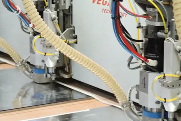
In reality, a PCB substrate is much like an ingredient in cooking: simply looking at the price tag is useless; you need to know how to pair it correctly. I’ve handled countless projects where top-tier materials were used, yet the entire batch of boards ended up scrapped because the manufacturing process—specifically the fabrication stage—fell short. This is particularly true for substrates requiring specialized processing techniques—such as certain fluoropolymers. While their datasheet parameters may look impressive, during actual production, even slightly excessive plasma treatment can cause the dielectric constant to drift so wildly that it becomes utterly unrecognizable.
What truly determines signal quality are often those easily overlooked details. I once tested a 28GHz millimeter-wave circuit and discovered that the exact same RO4350B substrate yielded a 15% difference in insertion loss when fabricated at two different contract manufacturers. We later traced the issue back to an improperly controlled temperature profile during the lamination process, which caused microscopic voids to form within the dielectric layer. This kind of problem is completely invisible if you rely solely on the material datasheet.
Nowadays, many people blindly chase after ultra-low Df (dissipation factor) values, forgetting that impedance matching is the true soul of the design. I once encountered a truly absurd design: they were using a substrate costing thousands per meter, yet they spaced their vias so haphazardly—like dancers in a public square—that signal reflections were severe enough to turn the board into an echo chamber. In truth, sometimes using standard FR-4 combined with a precise stack-up design proves far more reliable than blindly throwing money at the problem—especially when your routing density is so high that it necessitates extensive via placement.
I recently handled an interesting case where a client insisted—mimicking major industry players—on using ultra-low-loss materials for a 100G optical module; consequently, the cost skyrocketed to three times their original budget. We subsequently revised the design from an 8-layer board to a 10-layer board; by increasing the thickness of the ground planes, we were actually able to achieve superior return loss performance using only a medium-loss substrate. The key lies in spending every dollar of the budget precisely where it matters most—on the critical elements that genuinely impact performance—rather than blindly “stacking” expensive materials.
Ultimately, selecting a PCB substrate is like choosing a partner: simply looking at a resume isn’t enough; you have to put it to the test to see if it’s a good fit. Some materials boast impressive parameters but are overly delicate—their performance plummets at the slightest hint of moisture—while others may look ordinary but are rugged and robust. Whenever I formulate a design solution now, I always start by having the factory produce a small batch of prototypes to verify the actual production yield; this provides far more tangible and reliable data than any simulation ever could. The future demand for high-speed computing will undoubtedly drive the need for material upgrades; however, I believe the industry’s more pressing need is to fully unlock the potential of existing materials. I have encountered far too many teams that swap materials as casually as changing clothes, yet haven’t even mastered the fundamentals of temperature compensation. Rather than chasing after the latest innovations, it is better to first push the tools currently at hand to their absolute limits—after all, even the finest ingredients rely on a chef’s skill to be transformed into a culinary masterpiece.
While recently organizing laboratory records, I stumbled upon an intriguing phenomenon: a decade ago, while we were still grappling with the stability issues of standard FR-4 substrates, the industry had already quietly begun shifting toward more sophisticated material selection. One particular project stands out in my memory: we needed to maintain signal integrity within a high-temperature environment. After experimenting with three different types of PCB substrates, we realized that the inherent characteristics of the material had a far more critical impact on the final outcome than the circuit design itself.
I recall that during the testing phase, we utilized a modified composite material that performed unexpectedly well in a high-frequency environment. This material not only resolved our thermal dissipation issues but also ensured exceptionally stable signal transmission. It was at that moment that I truly understood why some of my peers are so meticulous about their choice of substrate materials—indeed, that choice can ultimately determine the success or failure of an entire project.
Nowadays, I observe an increasing number of engineers paying close attention to the coefficient of thermal expansion (CTE) of their substrate materials—a detail that was frequently overlooked in the past. In reality, whenever a circuit board is subjected to temperature fluctuations, the material’s thermal stability is of greater importance than its electrical conductivity alone. I have encountered numerous instances where a circuit design was technically flawless, yet the yield rate for the entire production batch plummeted simply because the substrate material underwent minute deformations in response to temperature differentials.
As technology continues to advance, new materials are constantly emerging; however, what interests me most is how these new materials integrate with existing manufacturing processes. Some high-performance substrates developed in research laboratories, while boasting impressive technical specifications, struggle to gain traction in the industry because they are incompatible with the demands of mass production. This serves as a reminder that in our pursuit of technological breakthroughs, we must not lose sight of practical manufacturing realities; otherwise, even the most exceptional materials will remain confined to the pages of academic papers.
A recent project involving telecommunications equipment provided me with fresh insights into the nuances of material selection. We had initially planned to utilize a high-end composite substrate; however, subsequent testing revealed that a mid-range material—once subjected to structural optimization—was actually better suited for mass production. This experience reinforced my belief that an exceptional engineer, much like a chef who intimately understands their ingredients, must possess a deep understanding of the specific characteristics of each substrate in order to strike the optimal balance between cost-efficiency and performance.
As electronic products become increasingly sophisticated, the future trajectory of substrate material development warrants close attention. I anticipate that in the years to come, we will witness the emergence of more highly specialized, customized materials—substrates optimized for specific application scenarios rather than designed merely to serve as generic, all-purpose solutions. This trend places higher demands on engineers, requiring us to continuously study the characteristics of new materials to make the most appropriate choices.
Sometimes, when reviewing past design schemes, I discover that material choices once deemed insignificant now appear to be the very factors that determine a product’s entire lifecycle. This reinforces my conviction that, in electronic product development, the substrate material is not merely a carrier but a critical factor influencing overall performance—one that warrants a greater investment of effort in research.
While tinkering with high-frequency circuits in the lab, I noticed a common misconception regarding the selection of PCB substrates: the belief that one must use the most expensive materials to produce a high-quality product. In reality, the key to high-frequency PCB applications lies in proper impedance matching, not in blindly chasing after extreme specifications. Last week, I assisted a team developing a drone video transmission system with a design revision; initially, they insisted on using Rogers RO3003, a choice that immediately tripled their production costs. We subsequently adopted a hybrid approach—utilizing a modified FR-4 material for the impedance-matching layers in conjunction with a standard high-frequency substrate—and the results actually proved superior.
The true determinant of a PCB substrate material’s suitability often lies in the details. For instance, automotive radar modules demand stability within high-vibration environments, whereas medical devices prioritize the material’s long-term reliability under sustained use. During one testing phase, we discovered that a material touted as “high-performance” exhibited severe drift in its dielectric constant following thermal cycling—an issue that nearly caused a significant project delay. Consequently, whenever I now encounter promotional materials that focus exclusively on Dk/Df parameters, I approach them with a healthy dose of skepticism.
The margin for error in high-frequency design is actually much narrower than one might imagine. We once worked on a 5G small-cell base station project where a mismatch in the substrate’s Z-axis coefficient of thermal expansion (CTE) caused the BGA solder joints to crack during high-temperature testing. Such issues are impossible to detect by merely consulting a material datasheet; they require rigorous validation within the context of the specific application scenario. I have since adopted a standard practice: before committing to any new material, I subject it to three rounds of thermal cycling tests to verify its suitability.
Recently, my exposure to various cases within the defense industry has actually given me a fresh perspective on commercial high-frequency materials. The approach of achieving high-frequency performance on standard FR-4 substrates—by employing specialized processing techniques—offers highly valuable insights for the consumer electronics sector. After all, the operating frequencies of most products never even reach the millimeter-wave range; consequently, there is simply no need to pay a premium for performance capabilities that will never be utilized. The critical point is to clearly define the actual performance boundaries required by the product, rather than allowing oneself to be swayed by the marketing rhetoric of material manufacturers.
When selecting base materials, I prefer to work backward from the perspective of the complete system. For instance, I first establish the efficiency requirements for the antenna, then derive the loss budget for the circuit board, and only then do I match these requirements to specific material characteristics. This approach often leads to more cost-effective solutions; for example, in an IoT gateway project I worked on last year, we achieved a 40% cost reduction by using standard materials combined with structural optimization—a far better outcome than simply opting for high-end materials. Ultimately, high-frequency circuit design is a matter of systems engineering; simply “throwing materials at the problem” is the laziest possible approach.
PCB design—specifically material selection—can sometimes be a real headache. I’ve seen many novice engineers get fixated right from the start on flashy, high-spec parameters; however, the critical first step is to clearly understand the actual operating environment in which your circuit board will function.
Take, for instance, a recent automotive electronics project I worked on: the client initially insisted on using the absolute highest-end materials, which doubled the cost without offering any practical benefit. We subsequently shifted our strategy and selected a substrate with a moderate glass transition temperature (Tg). This solution successfully met the demands of the high-temperature operating environment while keeping the project within budget. For applications located near the engine compartment, for example, thermal simulations revealed that the actual peak temperature reached only around 130°C. Since our moderate-Tg material (rated at approximately 150°C) provided ample safety margin, there was no need to select a high-end material with a Tg exceeding 170°C.
Speaking of the Coefficient of Thermal Expansion (CTE), many people tend to overlook a crucial detail: the CTE values in different directions can have a significant impact. During a multilayer board test we conducted, we discovered that the thermal expansion along the Z-axis (thickness direction) nearly caused the vias to crack open. Since then, I have made it a point to pay close attention to this specific parameter whenever selecting materials. Specifically, the CTE in the X-Y plane is typically controlled within the range of 12–16 ppm/°C; however, if the Z-axis CTE exceeds 50 ppm/°C, the copper plating within the vias becomes highly susceptible to cracking during thermal cycling tests. We subsequently adopted prepreg materials with matched CTE properties, thereby limiting the Z-axis expansion rate to under 35 ppm/°C—a measure that resulted in a significant improvement in via reliability.
While the sheer variety of substrate materials currently available on the market can certainly be overwhelming, I firmly believe there is no need to blindly chase after the newest or most expensive options. Standard FR-4 material performs quite stably in many conventional applications, and its key advantage lies in its excellent cost-effectiveness. Of course, if you are designing high-frequency circuits or products intended for use in specialized environments, you must carefully select specific materials tailored to those needs. For instance, RF circuits require low-loss PTFE substrates, while high-voltage applications demand close attention to a material’s CTI (Comparative Tracking Index) value; these characteristics necessitate a targeted approach to material selection.
I recall an instance where I was helping a friend debug a circuit board, and the issue turned out to be moisture absorption by the material. The board had been left in the humid climate of southern China for two weeks; consequently, it blistered severely during the subsequent reflow soldering process. As a result, I now always factor humidity—the operating environment’s moisture level—into my designs, particularly for products destined for export to regions with varying climates. For example, when designing products for the Southeast Asian market, we prioritize substrates with a moisture absorption rate of less than 0.1% and incorporate a moisture-resistant coating process during the PCB surface finish stage.
In truth, selecting materials is akin to formulating a traditional Chinese herbal remedy: one must adhere to the principles of Jun-Chen-Zuo-Shi (the “Monarch, Minister, Assistant, and Envoy” hierarchy). Simply piling together every high-quality material available does not guarantee a superior product; the critical factor is aligning the materials with the actual requirements of the application. Sometimes, a simple and practical solution proves far more reliable than blindly chasing after high-end, premium options. For instance, in power supply modules, we might selectively employ high-thermal-conductivity aluminum substrates in critical heat-generating zones, rather than utilizing expensive metal-based substrates for the entire board. This approach effectively resolves thermal dissipation issues while simultaneously keeping overall costs under control.
Personally, I prefer to create a “material test board” before proceeding with formal prototyping, allowing me to evaluate several alternative materials side-by-side. Although this adds a bit of extra time to the process, it serves as a safeguard against potential issues that could arise during subsequent mass production runs. This type of upfront investment is, in my view, exceptionally worthwhile. These test boards incorporate key test structures—designed to assess factors such as thermal cycling resilience, dielectric strength, and peel strength—enabling us to use quantitative data to objectively compare the actual performance differences between various materials.
Ultimately, PCB design is a process that demands the continuous accumulation of experience. Every challenge encountered presents a learning opportunity, and over time, one gradually develops a personal intuition and methodology for material selection. The key is to maintain an open mind and remain willing to experiment with various combinations of solutions. For example, through participation in industry seminars, we gained insights into breakthroughs regarding the CAF (Conductive Anodic Filament) resistance of certain modified epoxy resins—advancements that have proven immensely beneficial for our high-density interconnect designs.
Oh, and there is one more detail that is often overlooked: even the exact same type of material may exhibit performance variations depending on the specific manufacturer. It is highly advisable to establish your own internal supplier database to meticulously record and track the actual performance characteristics of products from each vendor. This ensures that the next time we select materials, we have a more reliable basis for reference. We once encountered FR-4 materials from two different suppliers; although their nominal Tg values were identical, the actual measured dielectric constants varied by a margin of 0.2. This discrepancy has a significant impact on digital circuits with strict impedance control requirements.
In short, I believe that working in this field requires a flexible mindset—one must understand both theory and practical application. Every project is unique and demands a flexible approach to identify the most suitable solution. For instance, medical devices prioritize material biocompatibility and long-term stability, whereas consumer electronics focus on balancing cost-effectiveness with manufacturability.
Looking back now, the detours we took have actually become invaluable experiences; sometimes, failure teaches us far more than success. Take, for example, that incident where an entire batch of circuit boards had to be scrapped due to improper material matching; it prompted us to establish a more robust material validation process—a lesson that simply cannot be learned from textbooks.
Whenever I see someone agonizing over material selection for high-frequency circuits, I can’t help but chuckle. Those who treat a specific brand or model number as gospel have likely never actually soldered a circuit board with their own hands. My biggest project failure involved blindly following a trend by using so-called “low-loss” materials—specifically, over-engineering a 26 GHz millimeter-wave radar module by stuffing it with a top-tier PTFE substrate. The result? Costs skyrocketed threefold. Later, I discovered that the team next door had achieved the exact same performance metrics—meeting all specifications—simply by using modified FR-4 combined with a clever layout design.
The truly agonizing part isn’t the material parameters themselves, but the moment you slide the PCB into a metal enclosure only to discover that the dielectric constant drifts wildly with temperature—to the point of being utterly unrecognizable. I once tested a vehicle-mounted radar unit by freezing it overnight at -20°C, then heating it up to 80°C the next day; the entire impedance matching scheme went completely haywire. That was the moment I realized that the pristine Df value listed in the datasheet offers absolutely no comfort in the real world. For instance, in low-temperature environments, the dielectric layer contracts, causing the characteristic impedance to rise; conversely, at high temperatures, expansion causes the impedance to drop. This dynamic fluctuation can cause a theoretically precise 50-ohm transmission line to drift to 60 ohms—or worse—during actual operation. For phase-sensitive applications, such as phased-array radar, this is nothing short of a disaster.
Nowadays, I approach material selection much like picking out fruit: what matters most to me is whether the supplier is willing to provide samples so I can test them out and iterate through trial and error. During a recent prototyping phase, I requested samples of epoxy resin substrates—featuring five different glass fiber ratios—from a domestic manufacturer. Upon sweeping the frequency bands using a vector network analyzer, I discovered that one unassuming model exhibited signal loss below 40 GHz that was actually more stable than that of imported ceramic-filled materials—despite its theoretically much higher loss tangent. After repeated verification, I found that this stability stemmed from a more uniform weave pattern in the glass fibers, which effectively reduced electromagnetic field distortion caused by anisotropy. Such practical insights gained through experimentation are far more compelling than mere paper specifications.
Many people assume that high-frequency design is simply a matter of throwing money at expensive materials; however, I believe it is far more effective to first master the fundamentals of PCB layout and routing. I have seen far too many engineers use premium materials like RO3003, only to route their microstrip lines with sharp 90-degree corners—and then blame the material for the resulting signal loss. Rather than spending that budget on exotic materials, one would be better off iterating on the layout a couple more times or applying a thicker gold plating to the RF connectors. For instance, using curved transitions or mitered corners at bends can reduce reflection loss by more than 10 dB. Furthermore, increasing the gold plating thickness on connectors from 0.1 μm to 0.3 μm can boost their mating cycle lifetime by five times in humid and hot environments—a far more practical improvement than obsessing over reducing the substrate’s loss tangent from 0.001 to 0.0005.
I recently encountered an interesting phenomenon while working on power amplifier modules for 5G small base stations: variations in the clamping force applied to the heat sink can cause the PCB substrate’s dielectric constant to shift by more than 0.2. While such subtle fluctuations have negligible impact below 6 GHz, they are sufficient to completely destabilize the antenna’s Voltage Standing Wave Ratio (VSWR) at 28 GHz. Consequently, when selecting materials now, we prioritize the compatibility of the Coefficient of Thermal Expansion (CTE) over rigidly chasing the lowest possible loss tangent values. Through thermomechanical analysis, we discovered that when the CTE mismatch between an aluminum heat sink and the substrate exceeds 3 ppm/°C, thermal cycling generates micro-cracks that lead to electromagnetic field leakage. We ultimately resolved this issue by switching to a composite metal substrate.
Ultimately, a high-frequency circuit functions much like an ecosystem; rather than fixating on individual material parameters in isolation, it is far more productive to focus on how factors such as copper foil roughness, dielectric layer thickness, and pad geometry interact and complement one another. On one occasion, I even successfully designed a 12 GHz filter using standard FR4 material. The key lay in engineering the transmission lines with a tapered structure to ensure a gradual, smooth transition for the electromagnetic field—a technique that proved far more effective than simply swapping in some “magic” exotic material. In the actual implementation, an exponential tapered line was employed to facilitate a smooth transition of the characteristic impedance—shifting from 50 ohms to 70 ohms and then back again—thereby effectively suppressing higher-order harmonics. This design philosophy transforms energy that would otherwise be reflected into a controllable distribution of electromagnetic fields.
If you were to insist on my advice, I would suggest first producing a prototype batch using the cheapest materials currently at your disposal. You might discover that those theoretical losses you’re concerned about never actually become bottlenecks. The true bottlenecks often lie in places you least expect—such as oxidized connectors or resonance within the shielding enclosure. There was once a case during debugging where signal anomalies were detected; the root cause turned out to be a specific screw hole in the shielding enclosure, which had inadvertently formed a quarter-wave resonant cavity that absorbed energy at a particular frequency. The issue was resolved simply by switching to nylon screws—a far more cost-effective solution than replacing the substrate, which would have cost thousands of dollars per square meter.
Whenever I receive a new circuit board, I invariably begin by feeling its texture—that unique tactile sensation, lying somewhere between paper and plastic, is actually the result of a complex interplay between layers of materials. Many people assume that selecting a substrate is merely a matter of picking an insulating sheet of appropriate thickness; in reality, however, this seemingly ordinary component serves as the very skeleton of the entire circuit.
I recall the first time I designed a high-frequency circuit on my own; I used standard FR-series materials, and the signal attenuation was so severe it felt like trying to listen to someone speaking through a thick wall. Later, when I switched to specialized substrate materials, that same circuit suddenly performed with crisp clarity. It was at that moment that I truly grasped just how critical the material’s ability to constrain and guide electrical currents really is.
Nowadays, when I see engineers agonizing over parameters like dielectric constant or coefficient of thermal expansion, I often suggest they first return to the most fundamental question: What specific type of energy flow is this board actually required to support? Some projects require the substrate to act like a sponge, absorbing mechanical vibrations; others demand that it serve as a precise thermal conduit. I once worked on a drone project where the use of an excessively heavy metal substrate slashed the flight duration by a third; switching to a lightweight composite material instantly resolved that critical endurance issue.
What is truly fascinating is the synergistic interplay between different materials. For instance, certain resin systems—despite possessing only mediocre insulating properties on their own—can, when combined with specific fillers, withstand sudden, high-voltage surges. Conversely, some substrates marketed for their exceptional heat resistance may actually perform worse than standard FR materials when subjected to thermal cycling. Such insights are rarely discernible from a mere datasheet; more often, they require observation during actual soldering tests—specifically, checking the interface between the copper foil and the substrate for any signs of microscopic cracks.
My recent involvement in medical device projects has further underscored a frequently overlooked aspect: material biocompatibility. Certain flux residues can react slowly with the substrate, releasing trace amounts of gas—a fatal flaw for precision sensors. Consequently, whenever I select materials now, I always build in a 20% margin to account for these “hidden challenges”; after all, a circuit board is not an idealized laboratory model—it must breathe, vibrate, and age within the realities of the physical world.
Perhaps the most counterintuitive revelation concerns the misconceptions surrounding cost. I once opted for a lower-grade substrate to save 30% on material costs, only to see our post-sales repair expenses skyrocket to double the original amount. A truly superior substrate should act like an invisible butler: never interfering with the circuit’s operation, yet always holding the fort when a crisis strikes. The next time you run your fingers along the edge of a circuit board, take a moment to consider that within those mere millimeters of thickness lies a precise, intricate dance of energy, temperature, and time.
In the field of medical electronics, attention often focuses on complex algorithms;
After years of navigating the hardware industry, I’ve observed an interesting phenomenon:
As a practitioner in the circuit board manufacturing industry, I am keenly
- Эксперт в области мелко- и среднесерийного производства
- Высокоточное изготовление печатных плат и автоматизированная сборка
- Надежный партнер для электронных проектов OEM/ODM
Часы работы: (пн-сб) с 9:00 до 18:30