
Wireless Baseband PCB: The Overlooked Foundation That Determines Whether 5G Actually Works Under Real Load
After talking to a base station engineer, I found that 5G’s real
The Small Box Nobody Thinks About — and the Board That Decides Your Internet Experience
I have always felt that most people have no real concept of that small box tucked behind the TV cabinet or collecting dust in the utility panel. Yet it is precisely this device that determines whether your videos load instantly or spin in a loading circle. I have seen many people complaining about slow internet who would never think to look at this inconspicuous device as the source of the problem.
The most critical component inside it is the circuit board. The PCB that we talk about every day plays a far more complex role here than most people imagine. It is not simply connecting various chips together. When the optical signal from the fiber needs to be converted into an electrical signal that a computer or phone can recognize, signal integrity throughout that entire process depends largely on the design quality of this board.
I have spoken with engineers who work on these products, and their biggest headache is maintaining signal cleanliness in a high-frequency environment. Many areas are already rolling out two-gigabit or even faster broadband. When data travels this fast, even a slight interference or loss significantly degrades the experience. Sometimes when a user feels the network is unstable, it may not be the operator’s problem — it may be that this board inside the device has not handled certain frequencies well.
Doing this kind of high-frequency board genuinely requires finding an experienced supplier. An ordinary PCB factory might handle consumer electronics adequately, but when it comes to the communications RF section, the requirements are at a completely different level. A good RF PCB supplier must understand materials, understand impedance control, and must be able to anticipate process variation that may arise during mass production. This is not something you can resolve by simply drawing up a circuit diagram.
I remember helping a friend troubleshoot occasional internet lag at his home. The root cause turned out to be that the board used inside an early-model fiber modem was too basic to handle today’s dense data flows. Replacing the device made the problem vanish immediately.
Now many new application scenarios are extremely sensitive to network latency — cloud gaming and remote collaboration, for example — and these cannot be resolved simply by looking at bandwidth numbers. The signal processing capability inside the device is increasingly critical, and this circuit board is the physical foundation of all that capability.
Design Philosophy Matters More Than Material Grade
I have always felt that many people misunderstand the circuit boards inside fiber modem-type devices. The instinct that newer technology is always better is simply not accurate. I was once looking for a reliable RF PCB supplier to build some samples for a project involving high-frequency signal trace handling. The result? Several suppliers immediately recommended various high-end materials and complex multilayer solutions, as though not specifying expensive materials made them look unprofessional.
This reminded me of the GPON equipment era. Back then, the circuit boards were far simpler. The designs of that era emphasized practicality and manufacturability. Engineers spent significant time on layout and grounding strategies rather than depending on expensive materials. A classic example: using standard FR-4 board material, carefully designing microstrip line widths and spacing to control impedance, we successfully achieved stable gigabit transmission — at nearly thirty percent lower cost than the high-frequency board material solution the supplier had recommended.
There is an unfortunate tendency now toward chasing so-called “generational technical leaps.” As if every new generation of device requires a comprehensive upgrade in materials and processes across the board. But my own experience tells me this is rarely necessary. Especially for ONT devices used by most home users, stability and reliability are the first priority.
Complex multilayer boards mean more vias and inter-layer interconnects, all of which can become potential failure points, especially under long-term thermal cycling and minor mechanical stress.
I have seen far too many “upgrade for upgrade’s sake” designs. Engineers insisting on changing a four-layer board to six or eight layers because a new XGS-PON standard feels like it demands it. But in reality, if you carefully plan your routing and handle high-speed signal traces and power routing well, a four-layer board is often entirely sufficient in many cases. In a four-layer board, placing critical high-speed differential pairs on the top and bottom layers with complete reference planes, while putting power and ground planes in the middle two layers for excellent decoupling, typically satisfies 10G PON signal integrity requirements very well.
When Material Selection Alone Is Never the Whole Answer
When people discuss PCBs these days, there is a strong tendency to focus on materials — as though specifying some special low-loss substrate resolves all problems. Materials certainly matter. But I believe design philosophy matters more. How you arrange the layout, how you handle impedance matching details — these factors often have a greater impact than simply swapping materials.
I have seen designs using very expensive materials but with terrible layout, resulting in completely unacceptable signal integrity. I have also seen designs using ordinary FR-4 material but executed with great elegance, performing remarkably well. Avoiding right-angle traces in the RF area, applying ground shielding around sensitive traces, and making careful impedance continuity transitions at connectors — these design techniques sometimes deliver more significant and direct performance improvements than switching to high-end board material.
There is also the supply chain management question. If you specify a particularly niche board material or process, what happens if the supplier encounters problems? Will production be disrupted? These are questions that must be considered when actually making a product. This is why I increasingly lean toward solutions that have been market-validated — even if they do not appear to be the most cutting-edge. A mature supply chain means more stable quality, shorter lead times, and more competitive pricing — critically important for consumer network equipment deployed at large scale.
Stability First: The Real Priority for Home ONT Devices
At the end of the day, whether it is GPON or a more advanced PON technology, the ultimate goal is always the same: the network works stably and reliably. When designing an Optical Network Terminal PCB, it is worth thinking from this perspective rather than blindly pursuing technical advancement. After all, users do not care how many layers are in the board — they only care whether their internet is fast and stable.
This board needs to be stuffed into utility panels in thousands of homes, endure summer heat and winter dust accumulation, and potentially run for years without interruption. So its design philosophy has reliability as its first principle and stability as its second. PON protocols and MAC-layer processing capability are certainly important — but if the RF PCB supplier you select cannot even guarantee basic four-layer board process stability, or if the designed PCB drifts badly under temperature variation, even the most advanced chip solution is wasted.
I have seen early product problems where the root cause was almost never in the chip, but in the board itself. Using inferior board materials to save cost led to uneven signal integrity in mass production. Or the power supply design was too rough. The result was devices that mysteriously dropped their connection or rebooted. A good ONT PCB should be like a silent, reliable old partner — you almost never notice it is there, but it just keeps data flowing steadily.
Integration and the RF Section: New Demands
The MAC unit processing the PON protocol is now essentially integrated with the main control CPU. The biggest benefit this brings is actually reduced overall power consumption and heat generation. Previously two chips might have needed to work together cooperatively. Now one highly integrated SoC handles it all. This is actually a liberation for PCB layout and routing. Designers can put more energy into optimizing power distribution and thermal paths rather than agonizing over complex high-speed interconnects between two chips.
Challenges have not disappeared. User demands are increasingly sophisticated — not just stable gigabit broadband, but seamless mesh networking and low-latency game acceleration. This means the wireless RF section on the PCB has become unprecedentedly important. It is no longer an optional add-on feature but a core component of the user experience.
This places higher demands on RF PCB design and manufacturing: how do you handle high-speed digital signals, sensitive RF analog signals, and high-power supplies all within a constrained space? This seriously tests the comprehensive capability of design teams and the process capability of suppliers.
So in my view, the standard for evaluating ONT PCBs is changing. In the past it focused more on whether the device could accurately implement the protocol stack. Now it requires comprehensive consideration of long-term operational stability, interference immunity in complex electromagnetic environments, and overall thermal efficiency.
The Signal Chain Must Flow Smoothly End to End
I have always believed that a good Optical Network Terminal PCB design should be like a smooth, gently flowing river — not a stream of constant waterfalls. Your job is to minimize those unnecessary “drops” — impedance discontinuities and signal reflection points — throughout the entire signal chain. This requires the designer to have a thorough understanding of the complete path from the optical interface to every electrical interface, not simply knowing how to invoke simulation software.
This means deeply understanding the impedance discontinuities introduced by via structures, the symmetry control of differential pair routing, and the matching between connectors and PCB pads. A common misconception is over-reliance on auto-routing tools while ignoring the necessity of manually optimizing critical paths.
The point when true technical upgrading is necessary is when signal rates reach speeds where ordinary FR-4 material begins to struggle. Signal loss and dispersion effects escalate sharply at 25 Gbps or higher. But even here, material upgrading is only one part of the overall solution — and not necessarily the first step. A genuinely capable RF PCB supplier’s value lies not only in providing a board that meets parameters. They can analyze the entire signal chain and identify where the bottleneck may appear.
Could signal integrity be improved through layout and routing optimization, temporarily avoiding the need to upgrade to materials costing twice as much? This kind of engineering judgment is where genuine capability is tested. Through better differential pair routing, reducing via stub lengths, and optimizing reference plane continuity, signal performance can sometimes be improved by several dB within the existing material framework — sufficient to meet the next phase of requirements while deferring expensive material upgrades.
High-Speed Signal Behavior: A System Engineering Challenge
The performance of high-speed signals on a PCB is a systems engineering challenge.
Beyond the material’s dielectric properties, you must consider the laminate stack-up structure, copper foil roughness, and even the impact of solder mask ink. Sometimes a thoughtfully designed ordinary FR board circuit can outperform a poorly designed high-end board at high frequencies. Using ultra-low profile or reverse-treated copper foil can significantly reduce conductor losses. Carefully designed layer stack-ups provide better impedance control and shielding. Selecting appropriate, stable dielectric constant solder mask ink avoids unpredictable effects on high-speed signals.
At the 50G PON level, every trace segment, every via, and even the uniformity of each dielectric layer directly affects final performance. A subtle difference — such as when a board material supplier changes a batch number — can cause the entire link’s bit error rate to rise by two orders of magnitude. Behind this are the collective amplification effects of differences in resin systems, fiberglass weave patterns, and even microscopic copper foil roughness variations on high-speed signals — factors that were often overlooked in the lower-speed era.
Experience in manufacturing often matters more than technical specifications. A team willing to candidly share failure cases and improvement processes is typically far more trustworthy than one that only shows you successful samples.
Batch Consistency: The True Test of Any PCB Supplier
Many people believe that as long as sample boards look good, a supplier can be trusted. The reality is that what truly tests a supplier is not whether they can produce one excellent sample board — it is whether they can stably replicate that same quality one thousand times, ten thousand times.
Think about where these ONT devices end up. Some go into living room TV cabinets — reasonably comfortable environments. Others get stuffed into outdoor fiber access boxes where summer heat can bake the enclosure and winter cold can freeze through it. This places very practical demands on both PCB material selection and design.
I once visited a factory that truly did excellent work. Their workshop had nothing flashy — but every link in the chain was solid. Detailed records tracked every roll of board material from warehouse entry. Key parameters were monitored in real time on the production line. Even the smallest detected anomaly could be traced back to exactly which process step had deviated. This seemingly laborious persistence was precisely what made their batch supply remarkably stable.
Many purchasing decision-makers fall into a trap when selecting suppliers — over-weighting small decimal-place differences in technical parameter sheets. Technical specifications certainly matter. But I increasingly feel that those invisible “manufacturing fundamentals” are the true dividing line. The same design file given to different factories can produce completely different real-world user experiences.
SMT Assembly Quality Is As Critical As PCB Design
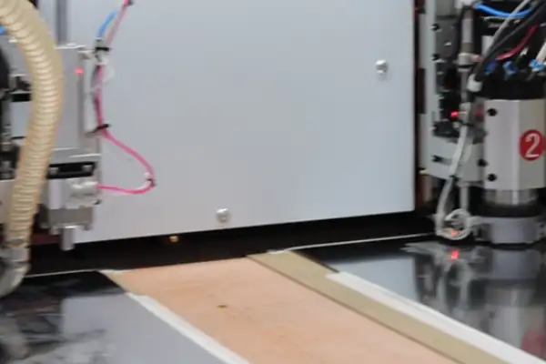
Good design alone is not enough. The manufacturing stage is equally critical. Especially SMT assembly quality directly determines whether those precision chips on the board can function properly.
Many ONT main control chips use fine-pitch BGA packages with densely arranged pins. SMT pick-and-place machines must have extremely high positioning accuracy to align those tiny solder balls precisely to pads. Any deviation — invisible to the naked eye — can cause cold joints or shorts.
I recall one instance where a production line switched to a new batch of solder paste. Because the viscosity parameters were not adjusted properly, some BGA chips developed pillow defects after reflow soldering — solder balls that did not fully melt and form reliable connections with the pads. This type of defect is completely invisible to ordinary AOI optical inspection — only X-ray fluoroscopy can detect it.
So now our requirements for SMT contract manufacturers go beyond just placing components correctly. We also require them to provide complete process control reports including solder paste printing thickness and reflow temperature profiles, ensuring every link is within controlled parameters.
Making highly integrated ONT devices is genuinely a systems engineering challenge. Any link in the chain slipping can cause overall performance to be substantially compromised. From initial PCB design and material selection through to SMT assembly, every process step requires an attitude of precision.
Finding the Right RF PCB Supplier: What to Look For Beyond the Spec Sheet
Choosing a PCB supplier is a bit like finding a life partner — you cannot just look at the list of credentials the other party has laid out. You have to see how things actually work in practice.
I had one particularly memorable collaboration. We had a new ONT project urgently needing prototype samples. One supplier — not the largest by scale — had their engineers proactively reach out within a few days of receiving our preliminary design. Not to discuss order volume, but to schedule a technical call to discuss our RF trace layout. They directly pointed out that in our original design, we had placed several critical RF signal lines too close to power traces in the pursuit of compactness. While the impedance calculations looked acceptable theoretically, in an actual high-frequency environment the crosstalk risk would increase substantially — especially when the PON module’s upstream burst transmission might trigger bit errors. Based on their experience with similar XG-PON ONT boards, they suggested adjusting the layer stack structure. No cost increase, but we gained an additional ground plane for isolation.
That experience clarified something for me: for boards like this — especially those with complex RF sections — what truly tests a supplier is not the impressive parameters in their brochure but whether their engineering team has real “feel.” This feel comes from having handled enough problem boards, having fallen into enough traps — for example, knowing which low-loss material has an unstable Dk value in which frequency band, or how minor differences in ENIG process affect high-frequency signal insertion loss.
So when I evaluate suppliers now, I do not just check whether they have ISO certification. I care more about whether they can clearly explain the three most difficult technical problems they encountered in the past six months and how they resolved them. A team willing to candidly share failure cases and improvement processes is typically far more trustworthy than one that only shows you perfect outcomes.
The optical network terminal market is already very mature. Competition long ago shifted from pure technology R&D to comprehensive manufacturing capability and reliability comparison. Your design can be as sophisticated as possible — it still ultimately comes down to a stable, reliable PCB board. Finding a partner who can think through problems thoroughly with you in the early stages, who is willing and capable of designing for manufacturability rather than simply processing from drawings, may provide more value than chasing the extreme limit of any single technical parameter.
After all, for products deployed at the scale of ONT devices, every successful mass production run represents countless instances of obsessive attention to detail and proactive anticipation of potential risk. And that capability is ultimately what matters to the person on the other end of the fiber.
After talking to a base station engineer, I found that 5G’s real
In the field of industrial automation, people often pay attention to AI
Ever wonder how your phone maintains a stable signal? It relies on
- Эксперт в области мелко- и среднесерийного производства
- Высокоточное изготовление печатных плат и автоматизированная сборка
- Надежный партнер для электронных проектов OEM/ODM
Часы работы: (пн-сб) с 9:00 до 18:30