
Heat Dissipation Challenges and Solutions in PCB Circuit Board Design
Circuit boards are more than just that green board in a phone
I think people in the hardware industry today may underestimate the importance of finding the right partner. Last year, our team experienced this firsthand when working on an edge computing device with an AI accelerator—we chose an ordinary multilayer PCB manufacturer for a prototype to save on budget, and ended up making a huge mistake. That factory couldn’t even handle the impedance control of a 4-layer PCB properly, let alone the 10-layer PCB we needed. We spent two months struggling with signal integrity issues without success.
In fact, truly professional multilayer PCB manufacturing is far more complex than simply stacking layers. Once, I visited a high-end factory, and their engineers showed me a very interesting case: for 10-layer PCBs, some manufacturers cram all the signal layers together, while they sandwich high-speed differential pairs like a sandwich between the power layers. This design improves signal quality by an order of magnitude.
Now, the power consumption of AI chips is becoming increasingly outrageous. I’ve seen some FPGA boards where a single chip draws 90 amps of current, which is a nightmare challenge for multilayer PCB power supply design. A manufacturer I worked with last year did a particularly clever job in this area; they used ultra-thick copper foil for the CPU power supply section and added a dedicated thermal management layer in the middle, making the stacked structure look like a work of art.
What surprised me most is that some top multilayer PCB manufacturers have started using AI for real-time process adjustments. During a visit, I noticed their electroplating tanks were equipped with sensor systems that automatically adjusted pulse parameters based on the chemical concentration. This dynamic optimization significantly improves yield compared to traditional fixed processes.
However, to be honest, the number of manufacturers in the industry that truly master high-end multilayer PCBs can be counted on one hand. Some small factories claim to be able to produce 16-layer boards, but upon closer inspection, the copper plating uniformity on their hole walls is absurdly poor. If their fundamental processes are inadequate, no matter how many layers they produce, it’s all for naught.
I increasingly feel that choosing a PCB supplier is like choosing a marriage partner; simply looking at the number of layers and line widths on the quote isn’t enough. You need to consider their ability to continuously iterate. After all, with the rapid pace of chip updates, a design that works today might need to be scrapped and reworked next year.
I’ve seen many people whose understanding of multilayer PCB manufacturing remains superficial. In reality, the quality of a circuit board often depends on the most inconspicuous details. Take drilling, for example; many people think it’s just a mechanical task, but the underlying materials science and chemistry principles are crucial.
I remember visiting a professional multilayer PCB manufacturer once. Their workshop displayed samples of various sizes, from the common 4-layer PCB to the complex 10-layer PCB. An engineer pointed to the densely packed tiny holes and explained that this seemingly simple drilling process actually requires precise control of the drill bit’s rotation speed and feed rate. Even a slight oversight can result in rough hole walls, affecting subsequent conductivity.
What truly surprised me was the hole metallization process. This isn’t simply copper plating; it’s a series of delicate chemical reactions. First, the hole walls must be completely clean, free of residual resin debris. Then, a special chemical solution is used to allow copper ions to adhere evenly to the hole walls. This process is extremely demanding in terms of temperature and time; a difference of a few degrees or a few minutes can cause uneven deposition.
Some manufacturers, to save time, skip certain chemical treatment steps, resulting in boards that quickly develop signal attenuation problems. This is especially noticeable in applications requiring high-frequency signal transmission, such as communication equipment or medical instruments, where even subtle quality differences become particularly apparent.
I’ve compared the processes of different manufacturers and found that good multilayer PCB manufacturers put a lot of effort into the formulation of chemical solutions. They have their own unique formulas to ensure that the copper layers are evenly covered in vias of different depths, which is especially important for high-density 10-layer PCBs.
Many customers nowadays only pursue low prices, neglecting these unseen process details, which is a real pity. A high-quality multilayer PCB depends not only on the number of layers and trace width, but also on the level of quality in these basic processes. After all, even the most complex designs ultimately rely on these fundamental skills.
Sometimes it’s a real shame to see ingeniously designed circuit boards suffer performance degradation due to inadequate manufacturing processes. Therefore, when helping customers select PCBs, I now pay special attention to the manufacturer’s actual process capabilities, especially their specific measures regarding drilling precision and chemical treatments. This often speaks volumes more than the numbers on the specifications sheet.
Ultimately, good circuit board manufacturing is like cooking; good ingredients alone are not enough, the chef’s skill is also crucial. Those seemingly ordinary processes hide true professional expertise, which is why the actual performance of multilayer PCBs from different manufacturers can vary so much, even for the same specifications.
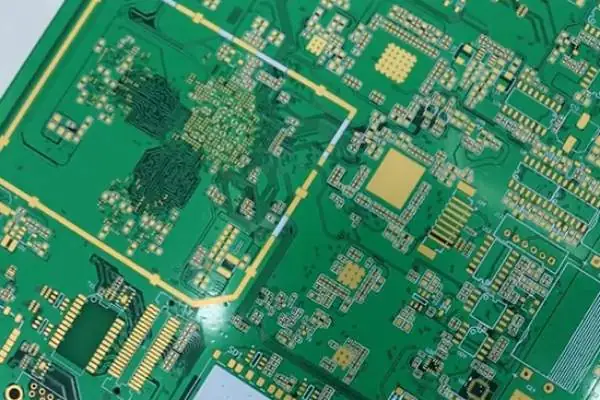
When I first started learning electronics design, I always thought the more complex the circuit, the more sophisticated it was. It wasn’t until I saw a disassembled 10-layer PCB that I realized true ingenuity lies in achieving stable and reliable connections within a limited space. This seemingly ordinary green board actually concealed a sophisticated three-dimensional transportation network. Each layer of circuitry has its own purpose: some are dedicated to power supply, others to signal transmission. They must maintain distance while working closely together. This reminded me of elevated highway systems in cities. Ground-level roads provide basic transportation, while interchanges at different heights allow for efficient traffic flow switching. This is probably the charm of multilayer design. For example, in high-speed digital circuits, the clock signal layer needs to be strictly isolated from noise sources, while the analog audio layer must be kept away from high-frequency switching power supplies. This vertical isolation capability is impossible to achieve with a single-layer board. Through blind vias and buried vias, signals between different layers can be precisely connected like an elevator, saving lateral space and reducing signal crosstalk.
Choosing a reliable multilayer PCB manufacturer is crucial. I previously worked with a factory that used simulation software to model signal transmission paths before production. Once, our 6-layer board design consistently encountered interference issues. Their engineers suggested sandwiching sensitive signal lines between two power layers. This change tripled the signal quality. Good manufacturers are like experienced architects; they not only turn blueprints into reality but also uncover hidden risks in the design. They also use flying probes to verify continuity in the finished product, much like conducting load-bearing tests on every newly built overpass. Experienced manufacturers can even improve high-frequency signal loss by adjusting the fiberglass cloth’s orientation; such process details are as important as considering the coefficient of thermal expansion and contraction of materials in construction.
Many beginners easily fall into the trap of pursuing excessively high layer counts. In reality, a 4-layer PCB can meet the needs of most consumer electronics products. I’ve handled many core boards for smart home devices that could operate stably with a 4-layer structure, yet they insist on stacking eight layers, increasing costs and production cycles. The real need for 10-layer PCBs often lies in scenarios with extremely high signal integrity requirements, such as medical imaging equipment or high-speed data exchange modules. In these devices, even slight timing deviations can cause the entire system to crash. For example, a CT scanner’s data acquisition board needs to process thousands of sensor signals simultaneously. The length difference between any two signal paths must be controlled within picoseconds, requiring compensation through delay matching lines in a multi-layer board. In contrast, a typical Bluetooth headset control board, with proper power and ground layer arrangement, can achieve an audio signal-to-noise ratio better than 100dB with just four layers.
Recently, while modifying a friend’s drone flight control board, I discovered an interesting phenomenon: adding two dedicated motor drive signal layers to the existing four layers not only improved flight stability but also extended battery life. This demonstrates that a well-designed layered structure allows for more efficient energy distribution—similar to how providing separate power cords for different appliances is much safer than cramming everything onto a single power strip. Sometimes, optimizing the circuit board structure is more effective than replacing expensive components. Specifically, the newly added independent motor control layer keeps the PWM signal away from the weak analog signal acquired by the gyroscope, essentially creating a soundproof wall between a noisy construction site and a precision laboratory. Simultaneously, dedicated layer routing reduces line impedance, resulting in a 40% reduction in instantaneous current drop during motor startup, directly translating into smoother hovering performance.
A visit to an automotive electronics exhibition gave me a new understanding of the reliability of multilayer circuit boards. Automotive equipment operates in environments ranging from -40°C to 85°C. Circuit boards that undergo rigorous testing use special lamination processes to ensure that the layers don’t separate due to thermal expansion and contraction. This reminded me of the mille-feuille pastries I played with as a child; their seemingly fragile structure actually contained immense resilience. Now, whenever I see the glossy circuitry in precision instruments, I feel that these thin boards bear the weight of modern technology. Manufacturers use high-TG-value FR-4 substrates, whose glass transition temperature can reach over 170°C, essentially giving the circuit board a fireproof suit. In the bonding stage, semi-cured sheets are laminated layer by layer, and the resin flow is controlled to fill micro-gaps. This process allows ten-layer boards to maintain a consistent dielectric constant even with drastic temperature changes.
Every time I see those complex circuit board designs, I recall the awe I felt when I first encountered multilayer PCB manufacturing. Back then, I always thought that compressing a dozen layers of circuitry into a single thin board was like magic.
I’ve seen many engineers obsessively focus on cost control for 4-layer PCBs, neglecting the impact of the design phase on the lamination process. A medical device client once came to us with dozens of revised drawings, insisting on achieving ultra-fine lines on a 10-layer PCB. During trial production, they discovered persistent misalignment of the core board—later found to be due to the design failing to account for the flow characteristics of the prepreg.
In fact, the biggest headache for multilayer PCB manufacturers isn’t the technical parameters, but maintaining stability during the curing process. I remember once visiting a factory where a senior engineer pointed to a cooling press and said, “This stage is like opening the oven door too quickly when baking a cake. Sudden temperature changes cause stress concentration, and even if it passes initial testing, delamination may occur after six months.”
Many young people today like to pursue the latest equipment, but I think the key is understanding the materials. For example, when making a 10-layer PCB, the temperature rise curves during lamination are completely different when using a standard core board and high-speed materials. We once tested prepregs from different manufacturers and found that differences in the flowability of some materials at high temperatures could cause linewidth variations exceeding 20%.
What impressed me most was an aerospace project. They required multilayer PCBs to maintain impedance stability after extreme temperature cycling. We experimented with seven different curing methods and finally discovered that the key issue wasn’t the lamination pressure, but rather the thickness control of the oxide layer during core board pretreatment. This detail is often overlooked even by many professional manufacturers.
Sometimes, looking at the laser alignment systems on the production line, I think these precision devices can easily make us forget the fundamental principles. It’s like focusing on smart kitchen appliances while cooking but forgetting that heat control is essentially about heat conduction. Truly good products require engineers who understand both design and manufacturing, knowing that the fundamental difference between a 4-layer and a 20-layer PCB in terms of design rules is not just about the number of layers.
Recently, there’s been an interesting phenomenon: more and more consumer electronics brands are starting to build their own PCB teams. They’ve found that outsourcing often encounters communication barriers—designers don’t understand lamination processes, and extreme factories don’t understand design intent. Perhaps in the future, good engineers will need a cross-disciplinary perspective, after all, circuit boards are never isolated components.
I’ve seen many people overemphasize complex calculation formulas and technical parameters when discussing multilayer PCB manufacturing. In reality, what truly determines the quality of a board is often something more fundamental. I remember once our team spent a lot of time struggling with impedance matching issues while designing a 10-layer PCB. Everyone was meticulously calculating trace widths and dielectric thicknesses to two decimal places. When the samples came out, we discovered the biggest factor affecting signal quality was an inconspicuous gap in the power plane. This gap was originally intended to accommodate a heatsink, but we hadn’t noticed during the design phase that it cut off the return path of critical signals, causing a discontinuity in the ground plane. Even worse, this defect was difficult to detect in simulation software because most models assume an ideal, complete plane. We eventually had to readjust the component layout, moving sensitive traces away from the split area and adding stitching capacitors to provide a high-frequency return path.
Choosing a reliable multilayer PCB manufacturer can certainly save you a lot of trouble, but don’t expect them to solve all design problems for you. One manufacturer we worked with before had incredibly detailed technical documentation, even clearly specifying the copper thickness tolerances for 4-layer PCBs, yet the first batch of boards still exhibited impedance drift. We later discovered that fluctuations in temperature and humidity during their storage environment caused the prepreg to absorb moisture. These are details you simply can’t detect unless you’re physically present at the site. If prepreg gets damp, it will generate micro-bubbles during the lamination process, which not only changes the dielectric constant but also creates localized stress during high-temperature reflow soldering. We later required the manufacturer to provide storage records for each batch of materials and added a vacuum baking process before feeding. This case made me realize that even the strictest incoming material inspection cannot compensate for negligence in one link of the production chain.
Many people think that simply connecting the traces is enough, but in reality, high-frequency signals are particularly sensitive when traveling through multi-layer PCBs. I once encountered a strange situation during testing—although all traces were designed for 50 ohms, actual measurements always showed a few ohms of deviation. After much troubleshooting, I discovered it was due to coupling interference from adjacent signal lines. Later, I developed the habit of proactively leaving extra space in critical areas, even if it seems wasteful in the design documents. For example, we implement “no-routing zones” around differential pairs, with spacing at least three times the line width. For clock signals, we also use grounding shielding vias to form an isolation ring. Although these measures increase board area, they effectively prevent eye diagram closure caused by crosstalk.
What truly changed my perspective was that redesign experience. I initially thought that ensuring symmetrical stacking would prevent warping, but the sample still showed slight deformation. After talking with the technical staff of the multilayer PCB manufacturer, I realized that in addition to balanced copper distribution, the matching of thermal expansion coefficients of different materials also needs to be considered. Now, I specifically check the uniformity of the heat dissipation path during every design review. For example, I use a grid-like copper layer under BGA components instead of solid copper foil to allow space for material expansion. I also avoid concentrating high-power components at the board edges to prevent localized temperature rise and stress concentration.
Regarding impedance control, I don’t think it’s necessary to rigidly adhere to theoretical values. In practical multilayer PCB applications, signal integrity often depends on the overall layout coordination. For example, the impact of via placement on the return current path is often underestimated. Sometimes, slightly adjusting the grounding method is more effective than simply optimizing the trace width. For example, placing grounding vias near layer transitions ensures the shortest path for return current. For high-speed signals, I use back-drilling technology to reduce via residue; this improvement is more effective in enhancing signal quality than obsessing over fine-tuning of trace width.
My recent work on a high-speed PCB has given me a new understanding of 10-layer PCBs—more layers aren’t necessarily better; the key is the proper allocation of functions across layers. Once, in pursuit of low impedance, I fragmented the reference layers too much, which led to EMC issues. Later, I switched to a simpler eight-layer structure, and the performance was more stable. My current approach is to prioritize ensuring each signal layer has a complete reference plane, even if it means sacrificing some wiring density. For particularly sensitive RF circuits, I allocate a dedicated ground plane to form a Faraday cage shield.
Ultimately, multi-layer PCB manufacturing is a process of continuous trial and error. Even the most precise calculation tools cannot replace actual debugging experience. The nominal ohm values are just the starting point; the real skill lies in anticipating and handling anomalies. For example, when I discovered insufficient timing margin in a DDR4 signal group, it was ultimately resolved by adjusting the decoupling capacitor layout on adjacent power layers. This kind of experience is difficult to gain entirely through simulation. Each trial production run is like solving a multi-dimensional equation, requiring a simultaneous balance between electrical performance, process feasibility, and cost control.
Every time I see those complex circuit board designs, I’m reminded of the confusion I felt when I first entered this industry. Back then, I always thought multilayer PCB manufacturing was simply stacking layers. Later, I discovered that the interplay between each layer was far more subtle than I imagined. I remember once designing a 4-layer board that experienced signal interference during testing. It took a long time to figure out that the crosstalk was caused by adjacent layers having their traces too close together.
Choosing a reliable multilayer PCB manufacturer can definitely save you a lot of trouble. One manufacturer I worked with had engineers who proactively suggested adjusting the stack-up structure and using more suitable dielectric materials to control impedance matching. This kind of professional advice is often more valuable than simply lowering the price.
Speaking of material selection, I’ve found that many people easily fall into the trap of blindly pursuing high performance. In fact, for a 10-layer board design in ordinary consumer electronics, using mid-range loss materials is perfectly sufficient. On the contrary, for cost-sensitive projects, excessively specifying ultra-low loss materials can lead to budget overruns. Once, I saw a client insist on using top-tier materials for a regular industrial control board, resulting in an overall cost 30% higher than expected.
In practical applications, I’ve found that loss control requires more focus on overall design optimization. For example, reducing the number of vias through reasonable routing planning, or adjusting trace angles to avoid sharp bends. These attention to detail are often more effective than simply upgrading materials. A communication module project I just completed last week is a good example—by optimizing the layout, the expected signal integrity metrics were achieved using ordinary materials.
There’s an interesting trend in the industry right now: more and more small and medium-sized manufacturers are starting to offer customized multilayer board solutions. This flexible service model certainly brings more possibilities to designers.
However, it’s important to note that some manufacturers, while offering attractive prices, may not meet the requirements for process control.
I recently encountered a manufacturer that claimed to be able to make 12-layer boards, but during the actual prototyping, we found that the interlayer alignment accuracy was completely substandard.
Ultimately, making multilayer boards is like dancing on a balance beam—you have to find the optimal balance between performance, cost, and reliability.
Sometimes the most expensive solution isn’t necessarily the most suitable; the key is to thoroughly understand the product requirements.
Now, for every project I undertake, I first spend time analyzing the application scenario before deciding on the appropriate multilayer structure and material combination.
This shift in thinking has saved me a lot of unnecessary trouble.
I’ve always felt that choosing a reliable multilayer PCB manufacturer requires a keen eye. I remember when I first encountered 10-layer PCB design, I found a manufacturer with a particularly low price, but it was a disaster—the BGA pads were delaminating and lifting. Later I realized their plating process simply didn’t meet the reliability requirements for multilayer PCBs.
Now, I see multilayer PCB manufacturing as like building with blocks; each layer requires careful consideration of the dielectric material and copper foil compatibility. Once, while testing a 4-layer PCB, I discovered poor signal integrity, and the investigation revealed uneven plating thickness on the inner layers, causing impedance abrupt changes. These kinds of subtle issues are invisible during prototyping; they only surface during mass production, revealing hidden defects across the entire batch of boards.
Actually, there’s a simple way to judge a manufacturer’s skill level: ask them to show a cross-section of the BGA package area. Reliable manufacturers will proactively show you the plating filling effect at the pad locations; those who use resin to fill vias often don’t dare show the cross-section. One company I worked with even used an electron microscope to inspect the copper wall thickness of each via—this meticulousness is a guarantee of quality.
While revising a friend’s design recently, I noticed an interesting phenomenon: many people blindly pursue 10-layer PCBs while neglecting the optimization of the basic 4-layer PCB. In fact, re-segmenting the power layer actually increased the wiring density by 20%. Multilayer boards are not simply about stacking layers; the functional planning of each layer is more important. Sometimes, reducing two layers can actually yield better results.
What frustrates me most is that some manufacturers exaggerate the in-pad via technology, only to find that the pad flatness doesn’t meet requirements at all. I’ve learned my lesson and now require impedance testing before ordering, especially for those micro-blind vias on high-frequency signal paths. Uneven plating of these vias renders the entire board unusable.
Truly professional manufacturers never rush you to make a decision. They spend time discussing the thermal design of each BGA pad and even suggesting changing certain vias to a combination of blind and buried vias. This kind of communication from the user’s perspective is more practical than any technology advertising, because the board is meant to be used in real products, not just displayed as a showroom sample.
Every time I see those complex PCB designs, I think a lot. Having worked in this industry for a while, I’ve noticed a rather interesting phenomenon—many people think multilayer PCB manufacturing is simply stacking single-layer boards. Actually, there’s a much deeper layer to it.
I’ve seen many engineers get stuck in the design phase because they always try to create a 10-layer PCB from the start, only to find that the cost and time exceeded their expectations. Sometimes, more layers aren’t necessarily better; it’s crucial to consider the actual needs. For example, a 4-layer PCB is sufficient for many ordinary products; there’s no need to blindly pursue high density.
Speaking of chemicals, I think many manufacturers rely too much on standard formulations and neglect the importance of customization. Different board materials require significantly different treatments; sometimes, a slight adjustment to the chemical concentration can solve major problems.
Packaging is another area easily overlooked. I’ve encountered many cases where the problem lies in the packaging design, but people always blame the PCB manufacturing. A good multilayer PCB manufacturer should intervene early in the design phase to anticipate potential problems for the client.
A recent project left a deep impression on me. The client initially insisted on using ultra-high-rise slabs, but after we suggested they start with the basic structure, they saved 30% on costs while still fully meeting performance standards. What does this illustrate? Blindly following trends is less effective than focusing on solid foundational work.
I believe this industry needs a pragmatic approach rather than solely pursuing technical specifications. Even the most advanced equipment will yield subpar results if attention to detail is lacking.
Circuit boards are more than just that green board in a phone
From disassembling old routers to visiting electronics manufacturing plants, I gradually realized
As an electronics enthusiast, I’ve come to understand firsthand the impact of
- Эксперт в области мелко- и среднесерийного производства
- Высокоточное изготовление печатных плат и автоматизированная сборка
- Надежный партнер для электронных проектов OEM/ODM
Часы работы: (пн-сб) с 9:00 до 18:30