
Why is the design of an ECG Monitor PCB far more complex than imagined?
Designing an ECG Monitor PCB is far more complex than it seems.
While chatting with friends working on base station hardware recently, I noticed a fascinating phenomenon. Many people think about MIMO in 5G as an algorithm or system architecture problem. But the issues that truly keep engineers up at night are the subtle physical details—like how traces are drawn on a PCB.
It might seem trivial. It’s just a circuit board. But I can tell you it’s not. When your antenna array scales from a few channels to dozens or even hundreds—what we call Massive MIMO—everything changes. Each signal travels through a segment of copper on the PCB before reaching the antenna. Even a tiny phase difference on each path, when summed across the array, can misdirect the final beam. It’s like a choir: if every singer is slightly off-beat, the harmony is lost. In Massive MIMO, each signal is a member of that choir.
So, engineers are focused on making High Frequency PCBs more precise. It’s not just about drawing finer lines. You need to consider the stability of the material’s dielectric constant, the effects of temperature changes, and the potential for interference between the many stacked layers. These issues weren’t as prominent at lower frequencies or with fewer channels, but now they are hurdles that must be overcome.
I’ve seen manufacturers simulating extreme conditions to achieve phase consistency—from -40°C to over 80°C and back—to see how signals drift, or how humidity affects material properties. It sounds tedious, but it directly impacts the base station’s coverage. Another key point: while new materials and processes are important, a design shift is also needed. In the past, we focused on individual component performance. Now, the entire Massive MIMO PCB must be treated as a single “signal path system,” where every segment is optimized together. For instance, to improve phase coherency on one path, you might need to adjust the lengths or shapes of other paths to achieve overall balance—a global perspective previously less necessary.
Ultimately, 5G’s challenge isn’t just speed; it’s forcing us to revisit those physical limitations we once ignored. The PCB, as the physical foundation for all theory, is more critical than ever.
I recently spoke with some base station designer friends and noticed a trend: everyone immediately points to materials when discussing the challenges of Massive MIMO PCB design. That’s correct, but I feel we might be thinking about it too simplistically. Many believe that using ultra-low-loss high-frequency materials will solve everything. I’ve seen projects where using expensive Высокочастотная печатная плата materials still yielded poor results. In MIMO systems, the truly difficult problems often aren’t just about the material’s quality but whether the entire system’s design philosophy has kept up.
For example, when you move to 64 channels, the system’s complexity doesn’t increase linearly; it’s more like an exponential growth. The interaction between each channel becomes incredibly complex; adjusting one parameter can cause issues in several other places. I remember testing a prototype where each individual channel signal was perfect, but the overall performance was poor. The problem was inter-channel synchronization—while each channel had good latency control, the relative delays were off by a tiny amount. This was negligible at 8 channels but became significant at 64, affecting the entire system. This subtle phase de-sync can ruin beamforming algorithms, preventing the signal energy from focusing precisely, thus severely reducing spectral efficiency and user experience. It’s like a band where each musician has perfect rhythm but they can’t play together—the overall performance suffers.
So, I think many discussions focus too much on the material’s parameters—like ultra-stable dielectric constants or ultra-low loss factors. These are important but are just basic requirements. The real performance determinant is how you build an architecture that coordinates all the elements on this foundation. This architecture must comprehensively consider signal integrity, power integrity, thermal management, and EMC to ensure the massive number of channels can coexist harmoniously at high speeds. Sometimes, over-optimizing one aspect to achieve ultimate signal quality can cause problems elsewhere. This art of balance is the core challenge of Massive MIMO design. For instance, choosing a thinner dielectric to reduce loss might weaken structural strength and worsen thermal challenges.
Moreover, different applications have very different MIMO requirements. Some prioritize coverage, others capacity or stability. This means there’s no single design approach that works for all. You must tailor the design, including PCB material and process choices, to the specific needs. For example, the priorities for antenna element spacing, PA efficiency, and cooling strategy differ significantly between a dense urban hotspot and a rural wide-area coverage application.
For cost-sensitive applications, you need to balance performance and cost, rather than just chasing the most advanced materials. This demands not just technical knowledge but also business needs and economic considerations. For instance, using more clever layout and grounding designs can achieve core specs with more cost-effective materials. So, instead of obsessing over materials, invest time in understanding what your system truly needs and how to find the optimal solution under various constraints. That’s the real test of a designer’s capability. Technology ultimately serves the application, not the other way around.
While chatting with some base station antenna engineers, I noticed another trend: everyone immediately focuses on high-frequency loss when discussing Massive MIMO PCB design. That’s correct, but I feel we might be over-emphasizing the material’s parameters. Many look closely at the perfect Df value of a specific material from a lab test. It reminds me of my student days, always seeking the ideal material. But product development is entirely different. A great datasheet doesn’t guarantee a good Massive MIMO antenna. The real performance-killers are often the overlooked details. For instance, will batch-to-batch material variations cause phase deviations across antenna elements on the same board? Could uneven temperature during lamination cause localized dielectric constant changes? These are real production issues, hard to avoid completely. I’ve seen teams spend a fortune on low-loss materials, only to get worse performance than a well-designed board with standard materials because of poor processing. It’s a shame.
I think there’s a misconception that material selection solves everything. In reality, there’s a long way from a good High Frequency PCB to a stable Massive MIMO system. How do you arrange those dense antenna units? How do you balance signal integrity with space constraints? How do you accurately evaluate the whole system’s performance? These are the real challenges. Often, the limitations aren’t high-tech issues but fundamental work done poorly. For example, if impedance control is imprecise, even the best materials are wasted. Or, if thermal design is neglected, material properties drift with temperature rise, rendering initial specs useless. So, I now focus more on the system’s synergy than the optimization of a single component. After all, Massive MIMO is a technology emphasizing overall coordination; the parts are interconnected. Good design makes rational trade-offs based on fundamentals and the application, not just chasing an extreme single parameter. This might require a mindset shift—relying less on formulas or standard answers and more on holistic system thinking.
I’ve been pondering Massive MIMO design recently and noticed an interesting trend: people dive straight into routing rules and stack-up details, which is important, but I feel this puts the cart before the horse. The core purpose of PCB design is to support the invisible world of wireless signals, allowing them to pass stably and clearly. If you don’t understand the signal’s intended path from the start, all that precise layout might just be solving a problem you’ve created.
Take channel design, for example. We always try to pack more channels onto a board for higher density. But this often leads to a paradox: packing them too close makes crosstalk a nightmare. I’ve seen designs that crammed RF traces together for ultimate compactness, only to face endless performance issues in testing. The underlying principle is simple: physical space limits are real, and signal interactions don’t disappear because you have good intentions. Sometimes, giving signals a little “breathing room” improves overall performance.
This brings me to a fundamental view of High Frequency PCB design: it’s an art of trade-offs and balance. You can’t have it all. Thinner dielectric materials for smaller size? You’ll face tighter process and cooling requirements. Want less crosstalk with a shield layer? It adds cost and thickness. I think the critical step is the work before you draw the first line. You must first understand the entire system’s signal flow: which parts are sensitive high-frequency, which are noise-generating power supplies. Conceptually partition these “functional zones” to form a macro-level isolation strategy. For instance, instead of obsessing over the 3W rule for a specific trace, step back and consider whether the whole area of that trace is physically isolated from nearby noise zones. Sometimes, smart zone planning can resolve many routing challenges. We design to ensure signals reach their destination cleanly and on time. Rules are tools, not the end goal.
When faced with a complex Massive MIMO PCB, forget the details for a few minutes and look at it from a simple signal perspective. Ask: “Is this path the least interfered with?” “Is this bend smooth enough?” You might have surprising insights. I’m not saying engineering rules aren’t important—they are. But above them, we need a more holistic, systems-level view. Get the big picture right first; detail work becomes more efficient. Otherwise, you risk falling into a local optimum trap. This approach has saved me a lot of effort on recent projects. I now spend more time with system engineers upfront, understanding each module’s true needs, and then doing a rough “city plan” on the layout. Once you’ve defined the industrial, commercial, and residential zones, designing the streets becomes much more straightforward.
I was recently chatting with some hardware veteran friends and noticed a common reaction: many engineers get nervous when they hear “Massive MIMO PCB” or “High Frequency PCB.” Everyone knows the performance requirements are high. But I think people might be overcomplicating things. Take material selection, for example. I’ve seen teams immediately go for the most expensive high-frequency materials. It’s not that they’re bad, but we often overlook practical questions. Can this expensive material be processed by your existing production line? Do the factory engineers have experience with it? I recall a project using a very advanced material, but the factory was unfamiliar with its processing parameters, scrapping the entire batch. The loss wasn’t just money, but precious time. So, I now lean towards considering practical production factors from the start.
Regarding hybrid lamination, it’s a key process in high-end PCB manufacturing. But I find many have only a superficial understanding, thinking it’s just pressing different materials together. It’s far more complex. How do you coordinate the different CTEs? How do you set the temperature profile to ensure bonding strength? It requires repeated trials. And we often over-technicalize these discussions, ignoring common-sense questions. Why use hybrid lamination? Is it for real performance needs, or just to appear more advanced? I’ve seen many “for-use-sake” cases where costs rose with little performance gain. It’s a waste of resources and a misunderstanding of design intent.
Regarding FR series materials, many think they are obsolete, but I disagree. Every material has its application. I recently used a heavily modified FR material on a project with good design, achieving full performance targets and excellent cost control. The client was very satisfied. I believe the goal is not to use the most advanced technology but to find the most suitable solution, balancing performance, cost, and manufacturability. Don’t just pile on high-end materials and complex processes; it often leads to products that are impractical and may fail in real-world applications. Stability and reliability are the top priorities.
I’ve always thought there’s a misconception about high-frequency PCB design: that you must use the most expensive materials throughout. That’s not the case. Those with real project experience know that localized solutions are often smarter. For Massive MIMO antenna boards, I’ve seen many insist on full-board high-frequency materials like PTFE, as if it’s the only way. But think about it: the sections truly sensitive to high frequency are often just the RF routing layers. The inner power and control layers don’t need such high performance.
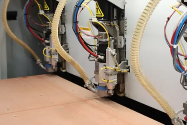
In one project, we used a specialized high-frequency material only on the RF signal layers and hybrid-laminated it with standard FR4 for the digital sections. The cost dropped by almost 30%, and performance still met industry standards. The manufacturing details are the real challenge. PTFE, for instance, is extremely smooth, making it hard for standard electroless copper to adhere. The factory must use plasma activation to create microscopic anchor points on the surface for the copper to bond. If this step fails, everything else is useless. The via stub issue is also a headache. At high frequencies, even a short unused copper stub can cause signal reflections. Good fabs use back-drilling to remove these stubs. I’ve seen fabs that couldn’t control this, resulting in boards with excessive high-frequency loss. Line width control is even more critical. In MIMO designs, those dense traces require extreme precision; a few microns can affect performance.
But I think the biggest challenge isn’t the process—technology always advances—but knowing up front where high-frequency materials are truly needed. Don’t just use high-end materials everywhere; it wastes money and adds manufacturing difficulty. I’ve seen designs considering regional use of different dielectric constants, which is an interesting idea. PCB design is never about “more expensive is better,” but about “fitness for purpose.” Especially in complex MIMO systems, you must distinguish critical paths that need protection from areas where requirements can be relaxed. This balancing ability is the real measure of an engineer’s skill.
I’ve always felt there’s a misunderstanding about 5G base station hardware design. Everyone discusses cool-sounding technical terms, but overlooks the most fundamental and tedious part: how a circuit board survives in the real world. I’ve seen too many perfect designs on paper fail in the field. For example, a PCB for a Massive MIMO antenna array might be designed with ideal lab parameters in mind. But once mounted on a tower tens of meters high, conditions change. In the north, winter temperatures can drop to -40°C, and in summer, direct sunlight can heat the enclosure to well over 65°C. Such temperature swings are hard to fully replicate in the lab. The real test of a High Frequency PCB isn’t its theoretical peak performance, but its ability to work reliably after hundreds of thermal cycles. In one project, all lab tests passed, but after three months of outdoor testing, signal quality degraded. We found that the board material had undergone slight deformation from thermal cycling—invisible to the eye, but a disaster for millimeter-wave circuits.
This taught me that MIMO system reliability isn’t just about stacking high-end materials. You need to understand how materials behave across temperatures, know which traces are sensitive to deformation, and realize how thermal design and mechanical mounting affect electrical performance. Sometimes the simplest reinforcement is more effective than complex material solutions. Many vendors promote their advanced technologies, but I value complete outdoor test data more. A board working in a lab oven isn’t impressive; one that survives all four seasons is. That’s why I’m skeptical of designs that trade overall reliability for a few percentage points of a performance spec. Such trade-offs are often not worth it for actual deployment. Good hardware should be like a craftsman’s work—not necessarily leading in every spec, but reliable anywhere. Especially for base station equipment meant to run for seven or eight years, long-term stability is far more important than peak performance. When you stand under the tower and look up at those equipment enclosures, you realize that all fancy technology must eventually serve the simplest purpose: don’t break.
I used to think that making high-frequency PCBs was just a matter of choosing the most expensive materials, sending off the design files, and waiting for the boards to arrive. Then a MIMO antenna project last year nearly tripped me up. We chose a low-cost supplier who confidently assured us they could handle Massive MIMO PCBs. The first batch of samples showed signal attenuation that was simply unacceptable.
The problem was their superficial understanding of high-frequency characteristics. They seemed to think that using Rogers material was the silver bullet. But the real challenge lies in handling the complex routing and stack-up structures. With so many channels crammed onto a single board for a MIMO system, this is no small feat. For instance, at millimeter-wave frequencies, even minor trace width deviations or uneven dielectric layer thickness can cause impedance mismatches and signal reflections, severely degrading beamforming performance. They may have only focused on the nominal Dk value of the material, ignoring its stability over frequency and temperature, as well as the fact that rough copper surfaces increase conductor loss. For the length matching in the antenna array feed network, they mechanically adjusted trace lengths without considering the different signal propagation speeds in different layers, causing phase errors that exceeded tolerances.
I slowly came to realize that when choosing a supplier, you can’t just look at their equipment list. You need to see if they truly understand your application scenario. Some manufacturers can make a beautiful simple double-sided board, but when you ask them to make a 16+ layer hybrid board with different material CTE matching, they fall short. I remember visiting a potential supplier’s facility, and their engineer actually asked me what effect dielectric constant tolerance has on phase consistency—and that question alone told me everything. A competent engineer should know that dielectric constant variations directly change the phase constant of transmission lines, leading to phase inconsistency between channels in array antennas or differential pairs, which worsens the signal-to-noise ratio and system EVM. They should be able to proactively explain how they manage this risk through material batch control, using specific resin systems, or by reserving tuning margins in the design.
A truly reliable partner will work through problems with you. They’ll proactively tell you what kind of crosstalk might arise from a particular routing style at a specific frequency band, or suggest adding ground vias in certain areas to improve isolation. For instance, they might point out that in dense stripline areas, using interleaved reference planes or embedded capacitance technology can optimize power integrity, reducing the impact of simultaneous switching noise on sensitive RF circuits. They might even suggest adding more realistic 3D via parasitic parameters to the simulation model based on their testing experience, bringing the design closer to actual manufacturing results. This kind of insight can’t be copied from a datasheet; it’s accumulated through learning from past failures.
Now, when selecting a supplier, I pay special attention to the similar projects they’ve worked on before. If they just give a vague “we’ve done many 5G projects,” I’ll press for specifics—what exactly the product was, what challenges they faced, and how they solved them. For example, was it an AAU board for a macro base station, or the RF front-end for a small cell? When dealing with thermal issues from high power, did they use special thermal via designs, metal-core substrates, or localized copper-embedded solutions? When handling the effect of via stubs on high-speed signals, did they use back-drilling technology, or did they optimize the via layout from the initial design? Those who can provide details are usually more trustworthy, because they’ve actually been through the wringer and learned from it.
Of course, price is always a factor, but I now consider cost after technical capability. A poorly designed high-frequency PCB might save you twenty percent on the board cost, but the time and effort spent debugging it later could be ten times that. And if the problem is only discovered after mass production, the losses are even greater. For instance, an impedance deviation caused by insufficient lamination alignment accuracy might force you to add tuning components or software compensation algorithms in the production stage, increasing BOM costs and potentially affecting product reliability and time-to-market.
Ultimately, this industry is a continuous process of learning and trial and error. Every new project brings new problems; no supplier can guarantee they’ll be perfect 100% of the time. But a good partner makes you feel you’re on the same side, working together to make the product right—not just a simple buyer-seller relationship. They actively participate in early design reviews, share design-for-manufacturing rules, and when problems arise, they work with you to analyze test data and find root causes and solutions from both process and design perspectives, rather than deflecting blame. That’s probably what I value most now.
I actually don’t like making PCB design sound mysterious, as if you need to understand a bunch of esoteric theories just to get started. Many people get intimidated when they hear “Massive MIMO” or “High Frequency PCB,” thinking it’s a field only for experts. But my experience is that many fundamental problems arise from the most unassuming places, like material selection and handling. For 5G equipment, everyone is chasing higher frequencies and more complex MIMO channels, which is correct. But have you ever noticed that sometimes, spending a fortune on top-tier high-frequency materials doesn’t necessarily lead to better overall performance than a board with ordinary materials but a solid design? The problem often isn’t the material itself, but how you use it. Hybrid lamination is a typical example. It sounds advanced, but at its core, it’s just pressing materials with different properties together. Yet many want to use the most complex multi-layer hybrid structures from the start, resulting in a host of signal integrity issues and skyrocketing production costs. I’ve seen many projects that didn’t need such complex stack-ups at all; a simple single-core or double-sided board, with proper layout and routing, could run perfectly well.
What really matters are those common-sense fundamentals: is the ground complete? Are there enough power decoupling capacitors? Have the traces inadvertently formed antennas? Without a solid foundation in these basics, even the best materials are wasted. High-frequency signals are certainly sensitive, but they follow the most fundamental laws of physics. A clean reference plane is worth more than any expensive low-loss material. I’m not saying materials science isn’t important. Massive MIMO antennas do require precise phase consistency, which places high demands on PCB manufacturing precision. But that doesn’t mean you have to be led by the nose by suppliers. Often, you can relax the stringent requirements on material tolerances by adjusting the antenna element layout or the feed network design. Making the design more robust is far more reliable than relying solely on the “perfection” of the materials.
Ultimately, hardware design is a systems engineering challenge. The PCB is just one part of it; it needs to work in concert with the RF front-end, filters, and even the overall system architecture. Don’t just focus on the PCB itself; think more about what role it plays in the entire chain. Sometimes, a change in perspective can make the problem solve itself.
Designing an ECG Monitor PCB is far more complex than it seems.
Facing frequent field failures of solar inverter PCBs? Our deep-dive analysis reveals
Industrial HMI PCB design goes beyond building a tougher board. It stems
- Эксперт в области мелко- и среднесерийного производства
- Высокоточное изготовление печатных плат и автоматизированная сборка
- Надежный партнер для электронных проектов OEM/ODM
Часы работы: (пн-сб) с 9:00 до 18:30