
How to Choose an Excellent Semiconductor Flex PCB Manufacturer?
While collaborating with a smart wearables team to select a semiconductor flex
I have always found integrated circuits to be fascinating; simply gazing at those densely packed rows of pins is mesmerizing. Sometimes, I’ll pick up a discarded circuit board and turn it over and over in my hands, examining the tiny chips mounted upon it. They resemble miniature cities—each pin serving as a connection point to a distinct functional district.
I recall a particularly interesting phenomenon I encountered while repairing a vintage radio. The radio had suddenly gone silent, so I began troubleshooting the issue. I eventually discovered that the problem stemmed from a poor contact in one of the pins on a specific integrated circuit chip. In reality, many faults that we perceive as complex often originate in these seemingly inconspicuous places. Those slender metal pins act like a city’s traffic hubs; if a single intersection becomes gridlocked, the entire system can grind to a halt.
The most miraculous aspect of integrated circuits is their ability to compress such a vast array of functions into a space no larger than a fingernail. I’ve watched people place a chip under a microscope to examine its internal structure; it truly looks like a detailed map of a precision-engineered city. However, the pin designs on many modern chips are becoming increasingly subtle—sometimes the traditional metal pins aren’t even visible anymore—which presents new challenges for repair and maintenance.
When it comes to repairs, I believe the most critical factor is understanding the chip’s underlying operating principles, rather than simply rote-memorizing diagnostic procedures. For instance, when I recently encountered an issue with a power management chip, I began by monitoring its operating temperature, then checked the condition of the surrounding components, and finally determined that the fault lay within the chip’s internal voltage regulation module. This “holistic-to-specific” approach to troubleshooting often proves to be the most effective.
Modern electronic devices rely increasingly on high-performance integrated circuits; sometimes, a single tiny mobile phone processor contains billions of transistors. This reminds me of the chips found in the vintage appliances I used to disassemble as a child—by comparison, those chips seemed as simple as building blocks. The pace of technological advancement is truly astonishing. Whether we are talking about simple power management chips or complex central processing units, their underlying design philosophy remains fundamentally the same: to pack the maximum amount of functionality into the smallest possible space. This, perhaps, is the true allure of integrated circuits; every time I study these tiny chips, I gain a renewed appreciation for the sheer ingenuity of electronics technology.
I’ve long felt that many people harbor a misconception regarding electronic products—they tend to focus their entire attention solely on the chips themselves. In reality, what truly brings these devices to life is the harmonious interplay of the entire system working in concert. Take the smartphones we use every day, for instance: you might pay close attention to the processor model, but few people ever stop to consider that the green circuit board lying beneath it is the true unsung hero working behind the scenes.
I’ve seen plenty of DIY enthusiasts spend a fortune on high-end IC chips, only to slap them onto a cheap, generic PCB. That’s akin to fitting a Ferrari with bicycle tires—no matter how powerful the engine is, you’ll never be able to unleash its full performance potential. Integrated circuits are undoubtedly crucial, but without a suitable circuit board to serve as their carrier and interconnect, they remain nothing more than expensive slivers of silicon.
I recall an instance where I helped a friend repair his audio system; he was convinced that a specific IC chip had burnt out. However, upon opening the unit, we discovered that the issue actually stemmed from aging traces on the PCB, which had resulted in poor electrical contact. This type of problem is incredibly common; quite often, device malfunctions have absolutely nothing to do with the chips themselves, but rather with the underlying substrate—the circuit board—upon which those chips reside.
Nowadays, many manufacturers heavily market the advanced capabilities of their chips. However, I believe we should be paying closer attention to the overall compatibility and synergy of the entire circuit system. For example, in high-frequency applications, even if you employ the most sophisticated integrated circuits available, a poorly designed PCB that introduces signal interference will inevitably compromise performance significantly.
Sometimes, watching device teardown videos can be quite fascinating. You’ll notice that the more high-end a device is, the more meticulous the craftsmanship of its circuit board tends to be. From the routing of traces to the choice of materials, every single detail is carefully engineered to optimize the performance of the integrated circuits it supports. This reminds me of the construction industry: even the finest building materials require a sound structural design to be transformed into a sturdy, habitable home.
I’ve recently been researching smart home devices and have noticed that some products—in an effort to cut costs—utilize circuit boards that are ill-suited to their components. The result is that the chips’ performance is dragged down, and the devices operate with chronic instability. This experience has actually deepened my appreciation for brands that are willing to invest the extra effort in the finer details; they understand that truly exceptional integrated circuits require an equally exceptional platform to unlock their full potential.
Ultimately, once you’ve spent enough time tinkering with hardware, you come to realize that the true test of technical proficiency isn’t measured by how expensive the chips you can afford are, but rather by how skillfully you can integrate a diverse array of components into a cohesive, functional whole. It’s a bit like cooking—while top-tier ingredients are certainly important…
Nowadays, whenever I choose electronic products, I pay particular attention to their internal construction. Sometimes, I’d rather opt for a device with slightly lower specs but solid build quality than take a risk on products that merely boast about their chip parameters. After all, no one wants to end up in that awkward situation where the chip is powerful, but the overall device performance is a total letdown.
I’ve recently been pondering a question: why do we always view chip manufacturing as something so mysterious? It actually becomes quite fascinating if you look at it from a different perspective. Those circuits—visible only under a microscope—are, in essence, no different from the building blocks we played with as children; the only difference is that the blocks have been replaced by transistors, and the glue by metal interconnects.
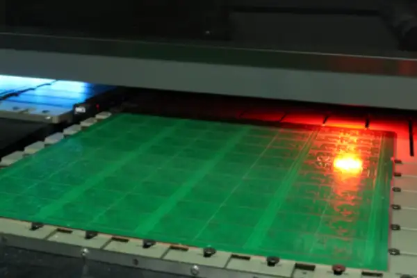
I recall visiting a semiconductor laboratory once and watching workers operate lithography machines in the “yellow room.” They jokingly remarked that their job was like embroidering on a silicon wafer—except the patterns they were stitching were a thousand times finer than a human hair. The way the wafers spun around inside the machines reminded me vividly of an old-fashioned record player.
The packaging stage, however, is what fascinates me the most. Just think about it: the very act of encasing a fingernail-sized chip inside a plastic shell is inherently full of contradictions. You have to protect the fragile internal structures while simultaneously ensuring there are channels for heat dissipation; you must guarantee electrical connectivity without compromising signal transmission speeds. That is far more difficult than simply applying a screen protector to a smartphone.
Many people today are discussing just how advanced 3D stacking technology is. Personally, I find the shift in the underlying integration philosophy to be the truly interesting part—moving from a flat, two-dimensional layout to a three-dimensional vertical structure is akin to upgrading from a single-story bungalow to a skyscraper. However, this design places much higher demands on thermal management—after all, heat doesn’t automatically rise on its own.
A friend once asked me why smartphones tend to slow down and become sluggish after prolonged use. It actually has to do with the aging of the integrated circuit board; the constant expansion and contraction caused by temperature fluctuations create microscopic cracks in the metal interconnects. It’s just like how water pipes eventually rust with age—except, in this case, the damage is invisible to the naked eye.
Speaking of which, it brings to mind an interesting phenomenon: many people assume that electronic products undergo such rapid cycles of iteration solely because of advancements in core technology. In reality, however, progress is often driven just as much—if not more—by materials science. For instance, the development of novel packaging materials can extend a chip’s lifespan by 30%—a contribution that is arguably even more significant than simply boosting raw processing speeds. I have always believed that the most critical breakthrough in the coming decade may not lie in semiconductor fabrication processes themselves, but rather in how we enable chips to integrate more seamlessly into our daily lives—much like how some smart home devices today already feature sensors woven directly into the fabric. This, to me, represents true integrated innovation.
Whenever I see issues arise with the tiny components densely packed onto an integrated circuit board, I find it quite fascinating. In reality, the problem often isn’t that the chip itself has failed, but rather that the issue lies with the solder joints.
I recall an instance where I was repairing an aging piece of equipment; the pins on the IC had developed a distinct intermittent connection with the copper contact pads on the PCB. From the outside, everything appeared normal, but a close inspection with a magnifying glass revealed tiny gaps. This reminded me of how people often tend to attribute such failures to poor chip quality, whereas I believe that, in many cases, the issue stems from inadequate soldering technique.
I’ve observed many novices overlook a critical detail when performing this delicate work: the formation of intermetallic compounds. If the temperature isn’t controlled precisely, or if the heating duration is insufficient, that vital connecting layer ends up being too thin—or worse, fails to bond properly at all. The result is that even a slight vibration or a significant temperature fluctuation can cause the entire connection to come loose.
On another occasion, I encountered a case involving a BGA-packaged chip where uneven heating during the reflow soldering process caused the solder balls on one side to fail to melt completely, while those on the other side were overheated. Consequently, the small component ended up tilting upward—standing almost like a tiny tombstone. I remember thinking at the time: if this were installed in industrial equipment, it would likely require rework in no time.
Regarding diagnostic methods, I feel that relying solely on measuring pin voltages can sometimes be misleading, as external components can exert a significant influence. For instance, a faulty capacitor might cause voltage readings to mimic an internal chip failure, when in reality, simply replacing that peripheral component resolves the issue. Therefore, I tend to prioritize inspecting the quality of the solder joints before even considering the chip itself.
Solder bridging—where adjacent connections short-circuit—is another common issue, particularly on high-density circuit boards. If too much solder paste is applied, or if the component alignment is slightly off, adjacent pins can easily bridge together. I once encountered a situation where a minuscule solder bridge caused the entire system to reboot repeatedly; it took me half a day of troubleshooting to finally pinpoint the root cause.
All in all, I believe the reliability of integrated circuit boards depends largely on these seemingly trivial soldering details, rather than on the relentless pursuit of high-end chips. After all, even the finest chip is rendered useless if its connections are unstable. My own experience suggests that investing the time to optimize soldering techniques is a far more practical approach than simply swapping in more expensive components. I’ve recently noticed that a lot of people are particularly fascinated by the tiny components found inside electronic devices. Integrated circuit boards, in particular, are actually quite a fascinating subject. Whenever I take apart an old mobile phone and see those intricate, dense circuits, I’m always reminded of my childhood days spent dismantling old radios.
I recall an interesting observation I made once while helping a friend repair a game console. If an IC chip on the motherboard was defective, the entire chip usually had to be replaced; however, issues with the circuit board’s traces were often much easier to fix. This brought a metaphor to mind: the IC is like the urban planning of a city center—once constructed, it is incredibly difficult to alter. The PCB, on the other hand, is more like the street network; if a specific route is blocked, you can often simply build a temporary bridge to bypass it.
The process of manufacturing silicon wafers actually demands far more patience than one might imagine. Last year, I visited a semiconductor laboratory; watching the technicians operate precision instruments inside the cleanroom, I suddenly realized just how complex the processes are that lie behind the lightweight mobile phone chips we hold in our hands. The photolithography stage, in particular—the process of transforming design blueprints into actual, functional components—feels just like embroidering a delicate pattern onto a silicon wafer.
Nowadays, there is much discussion regarding the autonomous production of semiconductor chips. In reality, every single stage—from IC design to the final product testing—is fraught with challenges. I once heard an engineer friend venting about how, during sample testing, their greatest fear is encountering issues with the wafer material itself; even the slightest defect can significantly compromise the yield rate of an entire batch of products.
PCB design, however, evokes a different feeling for me. It feels more akin to urban planning, requiring one to account for practical considerations such as signal interference and heat dissipation. I gained a deep appreciation for this while modifying an old audio system: if the layout of the circuit traces is poorly designed, even the most high-end components will be rendered useless. Sometimes, simply making a minor adjustment to the routing direction can result in a significant improvement in overall performance.
These experiences have led me to believe that, whether dealing with ICs or PCBs, the most critical factor is understanding the unique characteristics of each. Much like distinguishing between the main ingredients and the seasonings when cooking,
only by grasping the specific properties of the various components can one truly master the art of designing and repairing electronic devices.
Whenever I look at those exquisite circuit boards, I can’t help but smile—behind those dense, intricate networks of traces lie quite a few amusing misconceptions. Many people assume that integrated circuits are simply created by cramming more transistors into a chip and calling it a day—but that is just as naive as believing that you can build a house simply by having enough bricks. I’ve encountered engineers who treat a PCB as nothing more than a simple connector board—they assume that as long as the integrated circuits are mounted and power flows through, everything is fine. Consequently, the moment the product enters a high-frequency environment, it suffers from all sorts of signal interference. This issue often stems from a failure to realize that the PCB layout is, in essence, creating the operational environment for the integrated circuits.
I recall a time when I was debugging a piece of equipment and noticed that a specific module was consistently unstable. It turned out the PCB’s ground plane design had been handled far too haphazardly. Although the design utilized high-end CMOS chips, the routing failed to account for current return paths. This reminded me of cooking: no matter how premium your ingredients are, if the heat isn’t controlled correctly, the resulting dish will still taste terrible.
Nowadays, some manufacturers—in their quest for thinner and lighter devices—embed passive components directly inside the circuit board. While this approach certainly saves space, it becomes a major headache when a component needs to be replaced. It’s akin to burying water pipes inside a wall; when repairs are needed, you have to smash through the wall—a laborious and cumbersome process.
What I find most fascinating, actually, is observing how different manufacturers utilize the exact same chip. Some manage to push its performance to the absolute limit, while others struggle to get even its basic functions running stably. The gap between these two extremes often boils down to their understanding of the circuit board itself. After all, even the most sophisticated integrated circuit relies on the PCB to truly come to life; the relationship between the two is like that of an actor and a stage—neither can put on a show without the other.
Sometimes, looking back at circuit designs from twenty years ago is a truly intriguing experience. Back then, boards were cluttered with discrete components; nowadays, a single tiny chip can handle everything. Yet, this very progress has inadvertently led some people to overlook the fundamental importance of solid design principles.
Every time I see those tiny black squares densely embedded within a green circuit board, I’m struck by how fascinating it is. How on earth do these things enable a mobile phone to make calls or a computer to perform calculations? It’s actually quite normal for many people to struggle to distinguish between an Integrated Circuit (IC) and a Printed Circuit Board (PCB), given that the two almost always appear together.
I, too, was a bit confused when I first started out in electronics repair. I remember an instance where a neighbor’s radio went silent. I opened it up and noticed some rust on the pins of an IC; my immediate reaction was, “This chip is toast.” However, a veteran technician came over, took a look, and used a multimeter to test two traces on the PCB. He discovered that moisture had damaged the board, causing the copper foil traces to break. Replacing the chip would have cost several tens of dollars, but repairing the broken trace with a simple jumper wire took just five minutes. This experience made me realize that while the IC is responsible for the core task of processing signals, it is the intricately patterned PCB underneath that truly enables the smooth flow of electrical current. You can think of integrated circuits as the neurons of a brain, and the printed circuit board as the neural network itself—neither can function without the other.
Nowadays, many consumer electronics products prioritize a slim and lightweight form factor, often integrating the ICs and PCBs into a multi-layered, laminated structure. When I last disassembled an old mobile phone, I noticed that the chips on the motherboard appeared almost as if they had grown directly out of the circuit board itself. While this design certainly saves space, the repair costs become frighteningly high should anything go wrong. On one occasion, my fitness tracker malfunctioned after being exposed to water; the repair shop informed me that my only options were to either replace the entire motherboard or attempt a high-risk, layer-by-layer repair—precisely because the ICs and the PCB had become so deeply fused together.
This trend makes me feel a twinge of nostalgia for the modular designs found in old-fashioned radios. Although modern technology is far more advanced, for the average user, a device that allows for DIY component replacement offers a far greater sense of reassurance. After all, when every function is compressed into an integrated chip no larger than a fingernail, what we lose is not merely the possibility of repair, but also our tangible connection to the fundamental essence of the technology itself.
Perhaps this is the paradox of technological progress: the more sophisticated a device becomes, the more mysterious and inscrutable it appears to us. Yet, as long as we hold fast to that most fundamental principle—that even the most complex systems are ultimately constructed from functional units like ICs and connective substrates like PCBs—we will always be able to find a starting point from which to understand them.
I’ve always felt that many people’s understanding of circuit boards is a bit off track. The moment they hear “PCB,” they tend to fixate on the gleaming chips, as if the entire board’s soul resides solely within the ICs. In reality, however, what truly underpins the entire system are those humble components and the copper foil traces.
I recall an instance while debugging an industrial control motherboard where I encountered a peculiar phenomenon: the system would occasionally and abruptly restart during operation. Swapping out ICs from three different production batches failed to resolve the issue. It wasn’t until we sent the board to a laboratory for cross-sectional analysis that we discovered the root cause: uneven copper foil thickness within the inner layers. Fluctuations in the lamination process had resulted in abnormal impedance in a specific area of the circuitry.
That experience made me realize that a PCB is, in essence, a sophisticated ecosystem. While the IC is indeed responsible for computation and data processing, its stability relies entirely on the quality of the underlying circuitry. It is much like building a house: you can purchase the most expensive furniture, but if the foundation is poorly laid, everything else is in vain. This is particularly true for multi-layer board designs, where the copper traces—hidden deep within the board and invisible to the naked eye—often determine the overall reliability of the entire system.
Consequently, whenever I evaluate a new project, I now pay special attention to the manufacturer’s capabilities regarding inner-layer processing. Some smaller manufacturers, in an effort to cut costs, skimp on the quality of the copper foil material; the inevitable result is severely compromised signal integrity. Reputable PCB manufacturers, conversely, maintain strict control over the entire production workflow—from the base laminate to the solder mask—paying particular attention to the etching precision of the inner-layer circuitry, which directly impacts the transmission quality of high-frequency signals.
In fact, if one were to liken the IC to the brain, the PCB would be the nervous system. Even the most brilliant brain requires healthy neural pathways to function effectively; I have witnessed far too many instances where projects required costly rework simply because corners were cut on PCB manufacturing costs. Sometimes, seemingly insignificant details—such as the placement of vias or the partitioning scheme of power planes—can create a world of difference in the performance of the entire integrated circuit board.
This point was recently reinforced while I was helping a friend’s company troubleshoot a fault in a smart home gateway device. They were utilizing a mainstream, state-of-the-art chipset; however, during mass production, approximately 5% of the units consistently exhibited unstable network connectivity. The issue was ultimately traced back to the PCB manufacturer, who had upgraded the design from a four-layer board to a six-layer board but had neglected to adjust the inner-layer ground return paths accordingly. A minor modification to the copper-pours layout scheme was all it took to drive the failure rate down to zero.
Consequently, whenever my team and I discuss a new design strategy, we now make a conscious effort to allocate more time to the PCB design phase. Fundamental tasks—such as selecting the appropriate board thickness and meticulously planning the power plane hierarchy—may appear tedious, yet they prove far more effective than scrambling to resolve IC thermal issues or optimize firmware during the later stages of development. After all, once the current begins to flow, every single millimeter of copper trace silently influences the ultimate fate of the entire system.
I have always felt that many people harbor a fundamental misconception regarding the intricate little components found within electronic devices. Every time I hear someone refer to the small black blocks on a mobile phone’s motherboard as “the circuit board,” I can’t help but chuckle. That thing is clearly an integrated circuit, my friend! It’s about as absurd as calling an engine “the entire car.”
I remember the first time I took apart an old-fashioned radio; that was when I truly grasped the distinction between the two. The green board—crisscrossed with copper traces—is the actual circuit board; its job is to serve as the infrastructure, bridging connections and paving pathways for the various components. But those small squares with metal “legs” sitting atop it? Those are the true brains of the operation—the IC chips. Without the former, the latter are just a pile of scrap; without the latter, the former is nothing more than a pretty, intricate maze diagram.
Interestingly, many high-end devices today are merging these two elements in increasingly ingenious ways. Take Apple’s M-series chips, for instance: they integrate the memory modules directly alongside the processor. This design philosophy completely upends traditional circuit board layouts. Signals that once had to traverse the entire motherboard can now complete their interactions within a space no larger than a fingernail.
However, this trend toward integration brings with it new challenges. Last year, while repairing a graphics card, I encountered a tricky case where a cold solder joint on a video memory chip rendered the entire board irreparable. Ten years ago, a problem like that could be fixed simply by replacing the faulty memory chip; now, however, you’re left staring helplessly at a black resin-encapsulated integrated module. Technological progress has indeed made our devices more refined, but it has also raised the bar for repair work by several orders of magnitude.
Sometimes, gazing at the component-laden circuit board in my hand, I feel as though I’m looking at a miniature city. The IC chips act as City Hall, coordinating and directing operations; the capacitors and resistors serve as the infrastructure, ensuring the flow of energy; and those intricate traces are the crisscrossing streets and avenues. Only when each element performs its specific role can the entire city function harmoniously.
Ultimately, whether we’re talking about a simple radio or a complex smartphone, neither could exist without this exquisite interplay. The next time you peek inside an electronic device, take a moment to observe which parts are the “stage” and which are the “actors”—you’ll find it’s far more fascinating than simply misidentifying them.
I was recently tidying up my home when I stumbled upon an old mobile phone from ten years ago. As I pried off the back cover and gazed at the dust-covered circuit board within, a sudden realization struck me: this little device is, in essence, a microcosm of modern life. Those small black squares embedded in the board resemble a cluster of buildings within a miniature metropolis. Each chip possesses its own unique function: some handle computation, others manage power distribution. Yet, they can only fulfill their purpose because the PCB beneath them provides the reliable network of connections they need to operate. I recall a visit to an electronics factory where smart watch circuit boards were being tested on an assembly line. A worker pointed to a specific area, explaining that it was dedicated to processing fitness data. At that moment, a thought struck me: without a precise PCB layout design, even the most powerful chip would remain nothing more than an isolated island. This brought to mind the principles of urban planning—skyscrapers alone are not enough; a rational network of roads is also essential to facilitate the flow of resources.
I gained a profound appreciation for this concept last year when I attempted a DIY smart home conversion. The sensor modules I purchased kept malfunctioning. I eventually discovered that the issue lay in the solder joints on the circuit boards, which were too fragile; once I reinforced them, the system immediately stabilized. This experience taught me that integrated circuits and the boards that host them must function as a single, organic entity—much like the relationship between blood vessels and the blood flowing through them.
Nowadays, I view electronic products with a curious sense of X-ray vision. When my phone vibrates, I can visualize how the power management IC orchestrates the various components via the copper traces etched onto the PCB. When music plays through my headphones, I feel as though I can actually see the audio chip processing the signals. It is these collaborative systems—hidden beneath the plastic casings—that are the true protagonists.
Interestingly, this collaborative relationship is becoming increasingly sophisticated. For instance, many modern circuit boards now utilize flexible materials, allowing chips to be mounted in unconventional locations. It is akin to endowing electronic devices with an entirely new skeletal structure. This evolutionary trend serves as a reminder that technology is, and always will be, a dynamic force.
At times, I feel that our attitude toward electronic devices is overly superficial. In reality, what truly warrants our attention are those silently operating micro-ecosystems—the intricate worlds that integrated circuits construct upon their circuit boards. This, I believe, is the most captivating aspect of technology.
While collaborating with a smart wearables team to select a semiconductor flex
We often regard electronic products as a glossy whole, but ignore the
Many assume that choosing China for PCB assembly is solely about saving
- Эксперт в области мелко- и среднесерийного производства
- Высокоточное изготовление печатных плат и автоматизированная сборка
- Надежный партнер для электронных проектов OEM/ODM
Часы работы: (пн-сб) с 9:00 до 18:30