

What Documents Are Required for PCB Production: A Field Guide From Real Industrial Weighing Controller PCB Projects
Many engineers focus too much on technical parameters early on and overlook
Industrial IoT PCB Assembly: The Hidden Cost of Getting the Hardware Wrong
In conversations with factory engineers, a consistent pattern emerges. When Industrial IoT implementation comes up, people almost immediately start discussing cloud platforms or big-data analytics — as if getting data into the cloud is the hard part. Almost nobody volunteers to think about where the raw physical data originates. The answer is embedded PCBA modules: those unremarkable circuit board assemblies installed in equipment, pipelines, and facilities that quietly perform the first translation from the physical world into digital signals. When that translation layer fails, everything downstream fails with it.
Many people assume that industrial IoT PCB assembly is just a matter of specifying higher-grade components and thicker board material. That framing is too superficial. The real challenge is that the board you design today may spend the next five to ten years inside a vibrating fan housing, adjacent to a furnace, or in a humid underground conduit. It cannot be treated gently the way a phone can. It cannot be rebooted when something goes wrong. It must survive and function reliably, continuously sensing and reporting. The engineering starting point is not “how do we implement this feature?” — it is “how do we keep this feature working correctly in a hostile environment for a decade?”
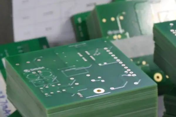
Why Consumer Electronics Thinking Fails in Industrial Environments
The most dangerous assumption in industrial IoT hardware is that a consumer electronics design approach, made somewhat more robust, will transfer to factory environments. It does not. A board installed in an industrial setting cannot be retrieved, inspected, or rebooted on demand. It must function correctly across conditions that no laboratory replicates well.
Consider what “environment” means for an industrial node. A cabinet in northeastern China in winter may accumulate frost on internal surfaces. A sealed control box in southern China under direct summer sun may reach internal temperatures of 80 to 90 degrees Celsius. These are not edge cases — they are routine conditions. Consumer-grade chips may fail to start up at subzero temperatures or produce data errors as thermal drift shifts sampling references. Substrate material matters for the same reason: standard FR4 in repeated thermal cycling can warp or delaminate. High-Tg materials — boards whose glass transition temperature exceeds 150 degrees Celsius — resist this dimensional instability in ways that standard materials do not. A Tg failure is typically gradual and invisible until a system collapses after an extreme weather event.
The electromagnetic environment in a factory is equally unforgiving. Motor drives, variable-frequency drives, welding equipment, and high-power switching loads running simultaneously create a complex interference landscape. Consumer electronics placed in this environment exhibit screen artifacts, communication dropouts, or inexplicable resets. For industrial SMT assembly, every aspect of EMC design — filtering circuit architecture, shielding enclosure placement, and grounding methodology — must be held to a more demanding standard. A simple RS-485 interface that requires only basic protection in a consumer product may need a three-stage defense in an industrial field installation: isolation, filtering, and surge protection capable of surviving the transient voltage spikes that large motors and welding arcs generate.
SMT Assembly Quality as a Long-Term Reliability Variable
The difference in mindset between consumer and industrial electronics is stark at the manufacturing level. Consumer electronics manufacturing accepts defect rates measured in parts per thousand — users can reboot, return, or replace products. When a data acquisition node on an automated production line loses communication for a few minutes, an entire batch of material may be compromised. The tolerance for failure approaches zero.
This means that every solder joint and every component in an industrial PCBA must be treated as a potential single point of system failure. Component traceability starts at incoming inspection: each batch entering the facility requires documented verification, and every chip placed on a board must be traceable to a specific supply lot. If a field failure occurs months after deployment, the ability to trace which material lots went into which specific units is not a compliance formality — it is the tool that enables rapid root-cause analysis and targeted corrective action rather than blanket replacement.
For BGA and other area-array packages, X-ray inspection is not optional. Joint formation quality — void content, ball height uniformity, absence of bridging — is entirely invisible to optical inspection and directly determines reliability under thermal cycling. Solder paste management is another frequently underestimated variable. Paste that has not been properly temperature-conditioned before use produces joints with different microstructure characteristics than joints produced from paste in its optimal condition. In sustained vibration environments, the difference in solder joint fatigue life between correctly and incorrectly managed paste can be significant. One case that illustrates the stakes: a food processing facility deployed humidity monitoring nodes using low-cost PCBA assemblies to reduce procurement budget. Within six months, nearly a third of nodes failed. Disassembly revealed oxidation at component lead roots — caused by trace ammonium compounds in the facility air reacting with a standard no-clean flux residue that a conventional process would have left on the board. The maintenance cost exceeded the procurement savings by a factor of ten.
Reflow Profile Optimization for Mixed-Thermal Boards
The reflow temperature profile is where the most technically demanding assembly decisions concentrate for industrial IoT boards. Standard automated profiling from nominal component thermal mass assumptions is inadequate when a board carries both large-mass power components and temperature-sensitive precision devices simultaneously.
A BGA processor package and a 0402 bypass capacitor mounted centimeters apart have thermal mass ratios that can exceed twenty to one. A profile that achieves adequate liquidus temperature at the BGA may expose the small passive to thermal stress beyond its internal material tolerance. The reverse — protecting small passives — may leave the BGA with insufficient reflow time, producing cold joints that pass immediate electrical testing and fail after thermal cycling in service.
Thicker copper layers on circuit boards exacerbate this problem. Copper layers two ounces or more thick absorb heat much faster than standard copper layers. If the solder joint profile doesn’t account for this thermal mass difference, solder quality will vary across the entire board; some areas will form optimal solder joints, while others may oxidize due to insufficient reflow or excessive dwell time. For these types of circuit boards, the appropriate calibration method is to perform actual measurements of the specific circuit board design using thermocouples under production conditions, rather than calculating the nominal profile.
The correct approach is DFM review participation by process engineering before any file is released to fabrication. Experienced process engineers identify pad designs that create paste volume problems, component placements that obstruct rework tool access, and missing process edges or fiducials — catching manufacturing risks at the point where they are cheapest to address.
Conformal Coating and Environmental Protection
For industrial IoT devices deployed in humid, corrosive, or particle-laden environments, conformal coating is not optional finishing — it is a functional component of the design. The material choice matters as much as the application. Acrylic coatings provide reliable general moisture protection and support rework, but have limited chemical resistance. Polyurethane coatings provide stronger protection against moisture and specific chemicals but require controlled application conditions and are more difficult to rework. Silicone coatings provide excellent flexibility through wide temperature ranges, making them appropriate for applications with significant thermal cycling where coating flexibility prevents stress cracking.
Application quality matters more than material selection if the process is undisciplined. Coating applied too thin in some areas provides no protection. Coating that covers connector contacts, test points, or heatsink surfaces creates secondary functional problems. Inconsistent coverage with bubbles or uncured regions provides moisture channels rather than barriers. Selective coating systems — automated dispensing or selective wave equipment — achieve the precise coverage that manual spray-and-mask processes cannot consistently replicate across production volumes.
Potting — full encapsulation in a protective compound — provides the highest environmental protection but eliminates repairability. For deployments where the expected service life exceeds the practical repair timeline and environmental severity justifies the protection level, potting is the appropriate choice. For applications where field serviceability is important, conformal coating at an appropriate protection level is generally more suitable.
Mixed-Assembly Workflow for Industrial Board Cards
Industrial IoT boards frequently require both surface-mount and through-hole components — high-density digital processing and communications circuits alongside large-format connectors, power relays, and terminal blocks designed to handle significant mechanical stress. These component types have incompatible reflow requirements if treated identically.
The traditional wave soldering process exposes all components to a single thermal cycle — which means that sensitive SMT devices may experience two high-temperature cycles if they are assembled on the bottom side and subsequently exposed to wave soldering. A more controlled approach stages the process: all SMT components are reflowed and functionally validated first, then through-hole components receive selective wave or hand soldering targeted specifically at their terminations. This adds production steps but ensures that each component type experiences only the thermal conditions appropriate to it.
One specific failure mode from this problem: a production batch of industrial motor monitoring nodes passed all incoming inspection criteria and functioned correctly in initial testing. Environmental chamber vibration simulation for four hours produced emerging BGA virtual opens — the joints visually appeared complete but had not achieved full metallurgical bonding due to insufficient paste volume at specific pads. The root cause was a stencil aperture design inherited from a consumer electronics reference design, not optimized for the board’s actual copper distribution. Catching this before field deployment prevented failure in units that would have been inaccessible for months after installation.
Scenario-Based Validation Beyond Standard Test Procedures
Standard test protocols provide a compliance baseline. They do not replicate the system-level conditions that produce field failures. The validation approach that consistently identifies problems before deployment is scenario-based: designing test conditions around the specific application rather than checking boxes against generic specifications.
For a cold-chain tracking node, adequate validation does not stop at minus-twenty-degree cold storage testing. It includes the thermal and humidity transition that occurs when a refrigerated truck door opens at a warm, humid loading dock — a rapid shift that stresses moisture-ingress barriers, power management circuits, and sensor response differently than any steady-state test. For a wireless device intended for factory deployment, a full-signal-strength reading in an open office environment means nothing. The relevant test is communication packet loss rate measured inside a metal-frame production facility with multiple motor drives and welding stations operating simultaneously. These scenario-based stress evaluations reliably intercept failures that standard chamber tests do not expose.
Wireless validation for industrial deployments deserves specific treatment. Many designs validate RF performance in benign electromagnetic environments and assume the result transfers to field conditions. It does not. One effective methodology used by development teams with field experience: place prototype units in a cooperating metal-working facility for one week of normal production operation and measure actual RF performance under those conditions. The data from this test is more predictive than any laboratory measurement.
Selecting a Manufacturing Partner for Industrial IoT Work
Equipment specifications establish a minimum capability baseline for a PCB assembly partner. The differentiation relevant to industrial IoT work lies in process understanding and problem-solving orientation.
The effective questions to ask a prospective supplier address whether they understand the application context, not just the technical specifications. A supplier who understands industrial IoT asks where the board will be installed — in an outdoor gateway or adjacent to a motor? The answer determines material selection and coating approach decisions that a generic capability assessment cannot reach. A supplier who proactively asks these questions before quoting is demonstrating a manufacturing mindset aligned with the application’s demands.
SMT placement accuracy specifications are a useful baseline indicator, not a performance guarantee. A supplier whose placement machines achieve stated accuracy but whose solder paste management is undisciplined, whose oven profiles are not validated for specific board designs, and whose floor temperature and humidity are uncontrolled will produce less consistent results than a supplier with slightly less impressive equipment specifications but disciplined process controls throughout. The consistency of output — across batches produced weeks apart, across different shifts, across small and large orders — is the measure that matters for industrial hardware.
Small-batch flexibility is a real value driver for industrial IoT development, but the right interpretation is not the fastest possible single-board turnaround. It is the ability to produce small pilot quantities using the same materials, the same process parameters, and the same inspection standards as volume production — so that design validation results actually transfer to production reliability. A supplier whose prototype process differs materially from their production process provides false confidence at the validation stage.
The relationship that produces reliable industrial IoT hardware over time is one where the manufacturing partner participates in design review, identifies risks before files are released, and maintains process documentation detailed enough to support root-cause analysis when a field failure occurs. A supplier who only executes finished files without contributing engineering judgment is not providing the full value the relationship allows. Identifying that kind of collaborative engagement during supplier evaluation is worth more than finding the lowest per-board price.
Industrial IoT deployments succeed when the hardware is invisible — stable enough that the system’s users focus on the data it provides rather than managing the devices providing it. Achieving that invisibility requires taking the PCBA seriously as an engineered product, not a commodity purchase. The difference between hardware that lasts five years in a factory environment and hardware that starts failing in the first six months usually traces back to decisions made long before the first unit shipped.
Many engineers focus too much on technical parameters early on and overlook
As someone who has worked in PCB outsourcing for years, I’ve found
Cramming a camera, amplifier, dual-mic array, and Wi-Fi radio into a palm-sized
- Эксперт в области мелко- и среднесерийного производства
- Высокоточное изготовление печатных плат и автоматизированная сборка
- Надежный партнер для электронных проектов OEM/ODM
Часы работы: (пн-сб) с 9:00 до 18:30
Get quote, solution or any question, Andre always here to help