
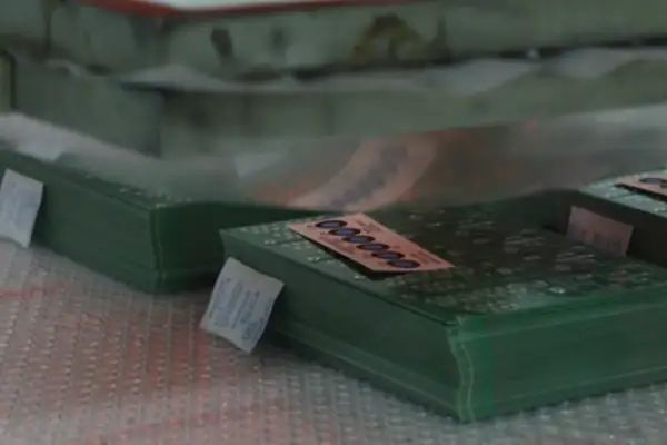
Solar Inverter PCB: Building Long-Term Reliability Against Salt, Moisture, and Thermal Stress
Facing frequent field failures of solar inverter PCBs? Our deep-dive analysis reveals
I have always found circuit boards that can withstand extreme environments particularly fascinating. I remember visiting a chemical plant control room in the north, where the outside temperature was minus twenty degrees Celsius. An engineer pointed to a screen on the operator console and told me the core PCB inside that device had been running stably for nearly ten years without a single failure. It struck me then that this required not just robust materials, but a product born from a profound understanding of industrial scenarios.
Many people imagine an industrial human-machine interface as simply a tougher touchscreen. In reality, from the very beginning of the PCB design phase, engineers operate on an entirely different set of principles. It is not designed for smoother swiping or more vivid colors; its purpose is to ensure that commands are transmitted accurately and without error, even in the worst possible conditions. In a workshop filled with dust or strong electromagnetic interference, the purity and stability of signal transmission are the lifelines of the system. This is not something that can be solved by simply stacking premium components; it demands an anticipation of the entire operating environment and the incorporation of design redundancy.
I have seen some well-designed consumer-grade products with sleek aesthetics and numerous features. However, once placed in the continuously vibrating cockpit of heavy machinery or in outdoor environments with extreme temperature swings, they quickly fail. A true Industrial HMI PCB must have reliability built into its very core. This reliability is not just a number measured in a laboratory; it is the ability to maintain full functionality in the face of voltage fluctuations, sudden temperature changes, or even accidental impacts. The difference is like that between a standard family car and a professional off-road vehicle.
Everyone is now talking about intelligence and data connectivity. For the industrial sector, I believe these new concepts must be built on a solid physical foundation. A reliable PCB is that foundation. If the underlying signal transmission can be corrupted, then any sophisticated data analysis or remote control loses its meaning.
So, in my view, the standard for evaluating a good Industrial HMI PCB is quite simple: when the operator needs it, does it provide a definitive and correct response every single time? This certainty forms the most fundamental layer of trust between human and machine. Without this trust, even the most advanced factory will suffer from inefficiency and potential risks due to operator hesitation.
This pursuit of certainty influences the entire manufacturing chain. From material selection to trace routing, from soldering processes to final testing, every step adds to the final reliability. Sometimes, to cope with a specific corrosive gas environment, a specialized coating process must be introduced—something almost never considered in consumer electronics.
Ultimately, technology exists to solve problems. Behind these seemingly mundane circuit boards, I see a pragmatic engineering mindset: understanding real-world challenges and then overcoming them, rather than chasing flashy, non-essential features.
I was recently chatting with some friends working in factory automation, and I noticed an interesting trend: they constantly complain about their equipment screens failing. Either the touch stops working, or the display becomes garbled. This reminded me of my own early mistakes when I first entered the industry—thinking I could just take a consumer-grade touchscreen, tweak it, and use it in a workshop.
The interactive interface in an industrial setting is a completely different story. Think about it: if you drop your phone, the screen might just crack, and you can get it replaced. But on a production line, even a few minutes of unresponsiveness can cause material backups or equipment damage. Under this pressure, the design philosophy for the circuit board must shift from “it works” to “it must not fail.”
What many people don’t realize is that the true determinant of reliability is often not the visible components, but the trace design hidden inside the multi-layer board. I have seen countless cases where using standard PCB processes to save costs led to signal interference issues within six months in a high-frequency vibration environment. Later, switching to HDI (High Density Interconnect) technology, which increased routing density, actually improved stability dramatically—it sounds counterintuitive, but it is true.
Of course, not every situation requires the most high-end solution. The key is to understand the device’s specific use case. For example, in a humid and dusty food processing plant, you might prioritize conformal coating over extreme miniaturization. In a precision instrument workshop, electromagnetic interference resistance might be more important than anything else.
Ultimately, the cardinal sin in industrial product development is “assuming.” I once worked on a project where the client insisted on using a consumer-grade chip for the control panel, arguing that the specs looked similar and it was half the price. The first batch of prototypes failed entirely during temperature cycling tests. The money lost was enough to redesign the entire project three times over. This lesson taught me that sometimes the most expensive solution is actually the cheapest in the long run.
I particularly want to warn engineers just starting out: do not be fooled by flashy specifications. The truly important parameters are often listed on the last few pages of the datasheet—operating temperature range, vibration tolerance, and the like. These are what determine whether a product can survive in a harsh environment.
Now, more and more factories are undergoing smart retrofits, but many managers have not yet realized the importance of the hardware foundation. They want to implement software systems first. In reality, if the underlying human-machine interface is not reliable, even the most advanced algorithms will be ineffective. It is like putting bicycle tires on a sports car.
Ultimately, designing industrial products requires a sense of respect. Every circuit board you design could be crucial to a production line’s operation or even worker safety. This responsibility is completely different from the consumer electronics mindset. It forces you to think one step further and test one more time at every detail. That is what makes this industry both the most challenging and the most rewarding.
I have always felt that many people misunderstand the screen on industrial equipment. They think it is just a larger version of a smartphone screen. That is far from the truth. I have seen too many examples of an entire production line shutting down because of an unreliable PCB. It is a terrible feeling. Imagine a workshop with dozens of workers waiting for a machine to resume operation. The problem often lies in the most unassuming place: the core board responsible for the human-machine interaction.
The true test is the environment, not how trendy the technology is. A factory is not a clean, tidy office; it is full of metal dust, oil, and massive sources of electromagnetic interference. If you take a standard PCB designed for a smartphone and put it in there, the touch might fail within days, or the screen might go black and reboot. This has little to do with the chip itself; the key is that the entire board’s design philosophy is fundamentally different from the ground up.
Take the simplest function—touch control—for example. We usually enjoy the smooth, responsive feel of a smartphone, wanting to tap it multiple times for a satisfying experience. But in a factory, workers wear gloves, and their hands might be covered in oil. What they need is deterministic feedback: press it, and it responds. That is why many high-end industrial HMIs still use the seemingly “outdated” 4-wire resistive touch technology or specially hardened capacitive solutions. The PCB design priorities for these solutions are completely different. It is not about recognizing complex gestures; it is about ensuring that every single tap is accurately captured, even under extreme conditions. This is why I pay close attention to whether a board is a true Industrial HMI PCB, rather than just any touchscreen module that can be powered on. The difference is like that between an off-road SUV and a city sports car—one is designed to run on all kinds of rough terrain, the other pursues ultimate speed on smooth pavement.
Many buyers only focus on processor clock speed or screen resolution, ignoring the most fundamental carrier platform—the PCB’s reliability itself. This is putting the cart before the horse. A good design will consider how to isolate power lines, how to route critical signals to avoid interference, and even how the pad surface finish will cope with long-term temperature cycling. These details are what determine whether a device will last three years or ten. Of course, ПЕЧАТНАЯ ПЛАТА HDI technology plays a supporting role here, enabling more compact layouts and reducing signal transmission issues, but only if the designer truly understands the needs of the industrial scenario. Otherwise, even the best process is useless.
Ultimately, choosing the right core board for the HMI is a choice about your attitude towards reliability.
I have always felt that the most overlooked aspect of Industrial HMI PCB design is the “human” element. We constantly discuss various technical parameters—routing precision, HMI response speed—but ultimately, this is an interface for people to use. If an engineer’s mind is full of data sheets while forgetting how an operator wearing thick gloves in a noisy workshop will actually press the buttons, then no matter how precise the board is, it falls short.
Take the touch experience, for example. Many design documents emphasize optimizing the touch signal’s noise immunity, which is certainly correct. But I have found that sometimes, in the pursuit of extreme signal purity—such as making the touch sensor traces overly complex or routing them to avoid all “potential risk zones”—new problems are introduced. For instance, the layout might become less compact, making the physical position of the touch area less than ideal, so the operator has to stretch to reach the “protected” button. Or, the fine-pitch routing required for multi-touch might be so delicate that even a slight production deviation makes future repairs and replacements difficult and expensive. In a factory environment, reliability and maintainability often outweigh the perfect theoretical data measured in a lab.
Speaking of specific routing, my view might be a little different. I do not believe that all high-speed or sensitive traces must be isolated and protected at any cost. Often, a well-thought-out, holistic layout with good reference planes is more effective than localized over-protection. The high-speed channels between the core processor and memory on an Industrial HMI PCB do indeed need careful routing to ensure signal integrity. But more importantly, the entire system’s power distribution network must be clean and stable. If the power supply itself is fluctuating, then no matter how perfectly length-matched you make the DDR differential pairs, the system might still fail due to a tiny voltage drop. Instead of putting all your effort into a few millimeters of trace length matching, it is better to first ensure that the entire board’s power delivery path is robust enough to withstand the common power disturbances found in industrial environments.
Another point is the choice of communication interfaces. Nowadays, many projects immediately specify the most advanced Ethernet protocols or wireless connections, thinking this is the hallmark of “Industry 4.0.” But in a real factory, many pieces of equipment that have been working diligently for ten or twenty years might only support traditional interfaces like RS485 or CAN bus. A truly “down-to-earth” Industrial HMI PCB should have the ability to connect the old and the new. It needs reliable isolation circuits to protect those classic serial communication interfaces, allowing the new HMI system to communicate smoothly with the workshop’s “veteran soldiers,” rather than forcing the entire workshop to upgrade for a single new panel.
Finally, let’s talk about the application of HDI technology. High-density interconnect technology can indeed make boards smaller, more refined, and integrate more functions. But it must be used with extreme caution in industrial products. Finer traces and smaller vias mean that under extreme temperature changes or continuous vibration, they can become weak points for reliability. Sometimes, using a slightly more traditional but robust process allows the board to survive longer in a cabinet full of oil, vibration, and thermal cycling. The design trade-off is precisely here—not blindly pursuing the highest technical specifications, but finding the solution that best balances performance, durability, and cost for that specific application. After all, a good Industrial HMI PCB should be one that you don’t even notice is there; it just quietly supports every clear and smooth human-machine interaction.
I recently worked on a touchscreen controller for a factory workshop and realized that industrial HMI circuit boards are a completely different animal from consumer electronics. Many people think, “Isn’t it just a control panel with a screen?” But there is a lot of depth to it.
Take the most basic material, for example. You certainly cannot use the same approach as for ordinary home appliances. The factory environment has huge temperature variations: the workshop can be scorching hot in the summer and freezing cold in the winter, and the machines themselves generate significant heat. This demands materials with high thermal stability, which is where high-Tg FR series materials come in.
What is Tg? You can think of it as a material’s “heat threshold.” Below this temperature, the material is in a hard, glassy state; once above this temperature, it begins to soften like putty. The Tg value of standard FR4 used in consumer electronics is likely around 140 degrees Celsius, which is far from sufficient for factory requirements. When the chips inside the machine start working, the temperature rises, and combined with the ambient temperature, it’s easy to approach or even exceed this critical point. Once the circuit board softens and deforms, problems arise. The most direct consequence is solder joint issues; due to slight deformation of the substrate, these tiny pads may crack, leading to insufficient solder joint strength or open circuits, as well as unstable signal transmission. Imagine if a touchscreen on a production line suddenly failed due to heat-induced deformation of the circuit board—the losses would be enormous.
That is why, for Industrial HMI PCBs, we now almost always use special FR4 materials with a Tg value of 170 degrees Celsius or higher. These materials are more expensive, but they raise the “heat tolerance threshold” through modified resin formulations, allowing the board to maintain sufficient hardness and dimensional stability under continuous high temperatures. It is money well spent; it is the foundation for ensuring the equipment can survive for years in harsh environments.
Speaking of signal processing, many advanced HMI functions are becoming increasingly complex, requiring the processing of large amounts of real-time data and images. This places “brutal” demands on the routing density of the circuit board. Standard double-layer or even four-layer boards simply cannot accommodate that many traces. This is where you need HDI PCB—High Density Interconnect boards. HDI technology allows for finer lines and smaller vias, packing more functional units into the same size board. This is crucial for making the entire control system compact, as installation space in factories is precious, and no one wants a bulky, heavy box. However, HDI processes are also more complex, with exponentially higher demands on materials and manufacturing precision. You need to find a truly experienced manufacturer to do it; otherwise, the yield rate can be frighteningly low.
Another easily overlooked point is the isolation design for the power management section. Industrial power grids are subject to a bewildering variety of disturbances—surges, pulses, spikes. If your power supply circuit does not have proper isolation and multi-stage protection, these disturbances will follow the power lines into the core control circuits. At best, the screen might flicker; at worst, the program could crash or the system could freeze. My experience is to treat the power section as an independent “fortress” in the layout, using physical separation slots or even a dedicated ground layer to completely isolate it from the analog circuits that handle weak signals, with ferrite beads or isolation chips in between to form a barrier, preventing noise from coupling through.
In short, making a qualified Industrial HMI PCB requires you to be a thermal expert, a materials scientist, and an EMC specialist all at once. It is not just about connecting chips and traces; you have to proactively defend against every possible harsh condition it might encounter. That is the charm of industrial-grade products—the challenges are huge, but the sense of accomplishment when you succeed is immense.
I recently chatted with some friends who design industrial equipment and noticed that their thinking when selecting circuit boards is completely different from ours in consumer electronics. We might be more focused on making things smaller, thinner, and cheaper. But their primary consideration is whether the board can survive a decade of abuse inside a machine. Take the circuit board for an industrial HMI, for example. Ambient temperatures can range from dozens of degrees below zero to over seventy degrees Celsius inside the workshop. In these conditions, looking only at the material’s glass transition temperature (Tg) is not enough.
Many people think that choosing a material with a high Tg value is the answer. But that is not the case. The coefficient of thermal expansion (CTE) of the board material in the Z-axis direction has an even greater impact. If this parameter is not well controlled, the copper plating inside the vias could be pulled apart after repeated thermal cycling, causing an open circuit, and the entire device would be dead. The repair cost would far exceed the price of a new board. So, many reliable suppliers now particularly emphasize how low their material’s Z-CTE is. This is far more practical than just touting a high Tg value.
Speaking of environmental humidity, it is another headache. Factory air is often full of oil mist and moisture. Standard materials used for a long time can suffer from Conductive Anodic Filament (CAF) failure, where copper ions migrate along the glass fibers, causing insulation failure. It sounds abstract, but it can indeed cause a device to short-circuit and shut down for no apparent reason. So, for industrial HMI material selection, CAF resistance has become a mandatory requirement. People are now paying more attention to whether the material supplier has detailed test reports for this, rather than just looking at the price.
Regarding the circuit design itself, consumer electronics often use very fine lines and thin copper foils for weight and space. But in industrial scenarios, the currents can be larger, and the traces need to handle stronger power delivery. This means you have to increase the copper foil thickness, from the common half-ounce to one or even two ounces. The current-carrying capacity and heat dissipation improve dramatically. Although the cost goes up, the stability is vastly different.
As for surface finish, we might use OSP or ENIG on phones—they are cheap. But for industrial panels that will be exposed to various gases and moisture for years, ENIG is almost the only choice. The thin layer of gold protects the nickel and copper underneath from corrosion, ensuring the contact points remain reliable for decades. Of course, the thickness and quality of the ENIG must be closely monitored; if it is too thin, it will not provide effective protection.
Ultimately, selecting a circuit board for industrial equipment is like solving a complex, multi-variable problem. No single parameter can determine everything. You have to weigh factors like temperature cycling, mechanical vibration, chemical corrosion, and current load together. Sometimes, achieving a higher reliability standard means upgrading the materials and processes for the entire board. The cost logic behind this is completely different from consumer electronics’ pursuit of extreme cost-performance. But that is the reality of the industrial sector. Every penny you save could become downtime on a customer’s production line in the future, and that is a cost anyone can calculate.
I recently helped a client adjust their industrial HMI control board design and noticed that many people have misconceptions about PCB layer count selection. There seems to be a default assumption that a 4-layer board is the “safe bet” for industrial applications—that four layers will solve everything. That is far from the truth, especially when dealing with complex human-machine interface signals. A simple 4-layer structure can become a bottleneck.
That client’s product originally used a standard 4-layer layout: signals and touchscreen interface on the top layer, ground and power in the middle, and some secondary components on the bottom. It worked fine initially. But when they wanted to add a new non-contact control module based on gesture recognition, problems arose. The data stream from the new module, transmitted on the same plane as the existing touchscreen commands, occasionally caused the display to stutter or false-touch events to occur. The engineers spent a long time investigating, suspecting a software problem.
We eventually turned our attention to the PCB itself. That new gesture recognition module was essentially a weak radio frequency signal acquisition and processing unit, extremely sensitive to noise and crosstalk on the signal path. In the original 4-layer architecture, the high-speed digital signal lines and the analog RF signal lines were physically separated, but they shared the same reference ground plane. When the touchscreen refreshed data intensively, the resulting ground bounce noise would couple through this common ground plane into the adjacent RF receive path, drastically reducing the gesture recognition accuracy.
We tried various routing optimizations with little success. Finally, we decided to re-evaluate the board structure. We did not jump directly to six or eight layers; instead, we first carefully analyzed the types and directions of the signals. I found the key issue was not the total number of layers, but that the return paths for critical signals were not isolated. So, we made a stack-up adjustment: we split the original second-layer solid ground plane into two separate regions, providing dedicated returns for the digital and high-frequency analog sections, and also partitioned the third-layer power plane more finely.
This change sounded minor, but the effect was immediate. The interference virtually disappeared, and the device became very stable. This taught me that in Industrial HMI PCB design, you cannot just focus on the “4-layer” or “6-layer” label. The real core is understanding the origin and destination of every signal in your system, especially those weak sensor signals or high-speed communication signals—they need clean, independent return paths. Sometimes, optimizing the allocation of your existing stack-up is more effective and economical than simply adding more layers.
Now, many engineers immediately think of HDI technology or more layers for complex functions. It is a valid solution, but costs rise sharply. For many mass-produced industrial devices, every penny must be spent wisely. My experience is to first exhaust the potential of a standard 4-layer board: carefully plan every power domain and ground plane split to ensure the shortest, cleanest return path for critical signals. This often solves more than 80% of interference problems. Only then should you consider whether more complex processes are necessary.
I often feel that many people misunderstand industrial HMI design. They think PCB design is just about fitting everything in and making it work. That is not the case. Take a recent project I worked on. They initially tried to save costs by using a 2-layer board for the prototype. The prototype worked fine in the lab. But once it was placed in a real site with a complex electromagnetic environment, the screen went haywire. They had no choice but to redesign it. The wasted time and cost far exceeded the initial savings on the board material. That is why I now place great emphasis on design robustness.
Regarding the specific board design, I believe you cannot make a blanket statement about how many layers are best. It depends on the specific application scenario. For example, some industrial HMIs need to process a lot of sensor data and display real-time graphics. This demands very high signal integrity. I generally recommend clients start with at least a 6-layer board. This allows enough space for proper routing of high-speed signals. For instance, in a 6-layer board, we can dedicate two inner layers as power and a solid ground plane, providing low-impedance return paths for the critical processor, DDR memory, and display interface, effectively reducing crosstalk and EMI. For high-speed differential pairs (like LVDS for displays) or high-frequency clock lines, impedance must be strictly controlled, and they should be protected with ground guard traces or by referencing adjacent ground planes—things that are difficult to achieve with 2-layer or 4-layer boards.
Another point I find particularly important is the design philosophy for the power system. Many people think that as long as the power supply is stable, that is enough. But that is not the case. Industrial sites often experience various voltage fluctuations and even instantaneous surges. If the power system is not designed robustly, the entire system can fail. My habit is to divide the different functional modules into independent power zones, each with its own filtering and regulation. Specifically, in addition to installing TVS diodes and varistors at the power entry for surge protection, I design independent LDO or DC-DC power trees for analog circuits (like high-precision ADCs), digital cores (like MPUs), and interface circuits (like RS-485). Each power zone is placed in a concentrated area on the PCB and connected via a single point using ferrite beads or zero-ohm resistors. This effectively prevents noise from propagating through the power path between different modules, avoiding contamination of analog signals by digital noise.
Regarding isolation, my view might differ from some. I believe isolation is not just about physical separation; it is about achieving true electrical independence. For example, even if you route a slot between high-voltage and low-voltage sections, if the ground planes are not handled properly, there will still be interference. I typically use the inner layers of a multi-layer board for isolation, rather than just drawing a line on the surface. This means that for circuits requiring strong galvanic isolation (like a non-isolated RS-485 interface from the internal system), I allocate completely independent, non-overlapping inner power and ground planes for the isolated sides in the PCB stack-up. At the same time, where a slot is cut in the board, ensure the copper is completely severed on all routing layers, maintaining adequate creepage distance. Sometimes, devices like transformers, optocouplers, or isolated power modules are needed, working together with the PCB’s isolation barrier to form a complete isolation solution from component selection to layout.
Now, many industrial devices have increasing real-time requirements. This presents new challenges for PCB routing, making HDI technology very important. It allows us to achieve more complex interconnections in a limited space while maintaining signal quality. However, this also places higher demands on design capabilities. HDI technology uses micro-vias and blind/buried vias to significantly reduce the parasitic effects of vias on signal paths, making high-speed traces shorter and more direct. For example, in the dense BGA area under a processor, HDI enables efficient fan-out of hundreds of pins and provides almost equal-length routing for critical high-speed buses, which is vital for data transmission stability and real-time performance. Of course, this also requires the designer to have a deeper understanding of signal integrity simulation and advanced manufacturing processes.
I believe a good industrial HMI design should be like a sophisticated ecosystem, where each part performs its own function and works in harmony. You cannot just focus on one local area; overall performance is key. That is why I always advise clients to plan thoroughly from the initial design phase, rather than waiting for problems to arise and then reworking.
Many people think that building an industrial touchscreen’s circuit board is just about stacking materials and technology. I do not think it is that simple. Consider the harsh environment of a factory workshop: dust, oil, temperature swings, and machines vibrating constantly. Can the design philosophy for such an environment be the same as for an office PC motherboard? I have seen too many people bring consumer electronics thinking directly into industrial settings and suffer the consequences. For example, someone might think using the latest HDI technology to make traces extremely dense will improve performance. But on site, within months, the fine traces break from vibration, or corrosive gases in the environment accelerate aging. In the industrial field, “better” is often not “more advanced,” but “more appropriate and more reliable.”
Speaking of SMT assembly processes, many people only focus on placement accuracy. But for industrial touchscreens, controlling the reflow soldering temperature profile is the real challenge. These boards often have a mix of components—some requiring high temperatures, others very sensitive to heat. You need to find a balance to ensure all joints are solid without damaging any components. I have seen factories that set aggressive profiles for speed, and yield looks good in the short term, but those marginal joints are the first to fail during long-term operation.
Another often-overlooked point is the PCB material itself. Standard FR4 degrades quickly in high-temperature, high-humidity environments. In particular, boards with insufficient glass transition temperature will deform over time, causing poor contact. Better industrial HMIs now use high-Tg materials. The cost is significantly higher, but the stability is in a completely different league. It is like building a house: if the foundation is not solid, no amount of luxurious decoration upstairs will help.
Protective coating is also a big topic. It is not just a matter of brushing on some conformal coating. You need to consider coating thickness uniformity, coverage integrity, and its impact on future repairs. Some areas need heavy protection, like around connectors; other sensitive areas cannot be coated too thickly, or it will affect heat dissipation or signal transmission. Truly good protection is the result of extensive testing and adjustment, not just following a standard process once.
In fact, what tests industrial product designers most is their understanding of the application scenario. Your PCB might have perfect lab specs, but in a real factory, you might encounter problems you never imagined—extreme EMI, or operators losing precision because they wear gloves. These must be considered during the design phase, not as an afterthought.
I believe the future direction of industrial touchscreens may not be about chasing higher integration or smaller size, but about doing more in terms of reliability and adaptability—like modular design for easy replacement of damaged parts, or adding more self-diagnostic functions to predict potential failures. After all, for a factory, the cost of downtime for maintenance is far higher than the price of the hardware itself. Sometimes, the simplest design is the most reliable. That is the deepest lesson I have learned over the years.
Every time I see the IP65 rating printed on the casing of an industrial touchscreen, I always feel it is only part of the story. The details that truly determine whether an industrial HMI circuit board can survive in a harsh environment are often hidden where you cannot see them. I have seen too many projects that only focus on enclosure sealing in the early stages, only to find the PCB completely ruined by condensation water inside. It is like installing the most solid security door on your house but forgetting to close the windows. For an industrial-grade HMI PCB, the design considerations must go far beyond consumer electronics. It is not just about being able to work; it is about maintaining stable performance for the next five or even ten years, even when the surrounding environment is full of oil, vibration, or extreme temperature changes.
Speaking of the circuit board design itself, HDI technology has now become almost standard for high-end industrial HMIs. This is not just to pack more functions into a smaller space; more importantly, it reduces long-distance signal traces, thereby lowering the risk of EMI. In a factory workshop full of variable frequency drives and large motors, the electromagnetic environment is unimaginably complex. A poorly designed PCB can easily become an antenna, either picking up noise or radiating interference to other devices.
I was involved in a project at a food processing plant that had a similar problem. Their early control panels would occasionally have a non-responsive screen or false triggers. After a long investigation, we found that interference from a large mixer motor nearby was penetrating the enclosure and affecting the signal integrity on the circuit board. We later re-designed the PCB layout with a more reasonable stack-up structure and grounding strategy, which completely solved the problem.
This brings me to a frequently overlooked aspect: the choice of IPC standard class. Many think that following the highest Class 3 standard is the only way to guarantee reliability. But my experience is that blindly pursuing the highest class can sometimes be a waste. Industrial scenarios vary widely. The reliability requirements for an HMI installed in a temperature-and-humidity-controlled clean room are completely different from one directly exposed to the high temperatures and dust of a foundry. For the former, a well-validated Class 2 standard product might be perfectly reliable, and it would be cheaper and faster to deliver. The key is to truly understand the specific environment your device will face and make a matching choice. This is not just a technical decision; it is also an economic trade-off.
Another thing that has deeply impressed me is the philosophy of testing. Many companies treat passing a series of standard environmental reliability tests as the finish line. For example, after completing hundreds of hours of high-temperature, high-humidity tests or hundreds of temperature cycles, they think the product is ready for market. But I think these standard tests are more like a starting point—a baseline to confirm the product has no obvious design flaws. The real test is in the actual application, under combined stresses that the test procedures cannot fully simulate. For example, vibration superimposed with thermal shock, plus sudden power fluctuations—this situation might happen every day in a real factory.
So, we now tend to favor a “beyond-the-spec” testing approach: after completing all mandatory standard certifications, we put the prototype into a simulated real operating condition and let it run continuously for months, recording every minor anomaly. This kind of testing often uncovers problems that isolated environmental tests cannot reveal. Ultimately, creating industrial-grade products requires a different mindset: it is not about pursuing extreme performance or flashy features, but about building stability and reliability into every design detail.
Recently, while chatting with some friends in industrial equipment, I noticed an interesting phenomenon: everyone is paying more and more attention to the PCB design of HMI products. In the past, they might have thought it was just a control panel with a screen. But now it is different! In many factory environments, EMI is extremely severe, with high-power motors or VFDs operating nearby. If your screen frequently flickers or suffers from false touches, the operators will be furious. So, designing a PCB for an industrial HMI now involves far more complex considerations than consumer electronics!
I have seen some projects that initially used standard multi-layer boards to save costs. But during field testing, all the problems emerged. Signal instability is a minor issue; the worst-case scenario is the board failing in a damp or corrosive gas environment. In that environment, you cannot maintain or replace it frequently. So, reliability must be built in from the ground up!
Speaking of which, I have to mention HDI technology. Many high-end industrial HMIs are now packing more and more functionality onto a limited board area. Traditional PCB processes might be struggling. HDI enables finer traces and higher interconnect density, which is very helpful for shrinking product size while maintaining performance.
But high density alone is not enough! The EMC requirements in industrial settings are almost draconian! I remember visiting an automated production line. The EMI noise generated by all the equipment running simultaneously was a cacophony! If your HMI does not have solid EMC protection, the data it displays might be jumping around! This is no joke! So, good industrial HMI PCBs now treat EMC as a core design metric from the start! For example, filtering at the power entry must be very clean; sensitive signal traces must be routed on inner layers and surrounded by ground planes; even connector selection and placement are carefully considered. These seemingly trivial details determine whether the product can work stably for ten or eight years on site!
I also think material selection is particularly critical! Standard FR4 might perform well in a standard lab environment, but in the real industrial world, with large temperature and humidity swings over time, the board might deform or its electrical performance might degrade. So, many manufacturers now choose higher-performance substrates. Although the cost goes up, from a total product lifecycle perspective, it is actually more cost-effective! After all, for a factory, the loss from equipment downtime is far greater than the cost of a circuit board!
Ultimately, designing a good industrial HMI PCB is about balancing many things: performance, cost, reliability, manufacturing feasibility, and more. It is not like consumer electronics, which can pursue extreme thinness or a cool appearance. For industrial HMIs, stability and durability come first! This requires the designer to have a deep understanding of the actual application environment. You cannot just draw boards in an office; you need to visit the field frequently to see the conditions under which the equipment will operate. Only then can you create a product that truly stands the test of time!
Many people think that sourcing an HMI board for industrial equipment is just a matter of finding a factory that can do high-density routing. I used to think that way too, but later I realized it is far too simplistic. What really gives you a headache is not the technology itself, but whether this partner you choose will still be around, and still be able to support you, ten or even fifteen years from now. That is the ultimate test of a supplier.
I have seen too many suppliers make grand promises. They show you their latest HDI PCB samples, boasting about how their line width and spacing can be pushed to the extreme, and what advanced packages they can support. That is all important, of course. But the problem is your equipment is meant to be used in a factory for over a decade; it is not a one-time transaction. If they can build it for you today, will they still be willing to stock materials for your “old” product in five years after they have upgraded their production line or changed direction? This is the most easily overlooked link in procurement decisions.
So, when I evaluate a supplier’s credentials now, I look at certifications differently. ISO9001 is a basic threshold, that goes without saying. I care more about how they view the substance behind these certifications. For example, a factory that has passed the automotive-grade IATF 16949 certification usually has a level of process rigor that permeates its other product lines. Their sensitivity to failure modes and process control is something that a factory with a consumer electronics background cannot easily replicate in the short term. But that is not all.
What I really want to understand is their material management philosophy. A good Industrial HMI PCB supplier should have a clear “long-lifecycle bill of materials” in their warehouse. They need to prove they have stable channels to source those components that may not be mainstream but are critical to the stability of your device, such as specific models of high-Tg materials or durable connectors. More importantly, do they have a mature alternate part qualification process? If a key component is suddenly discontinued, do they just throw up their hands and say, “No way, you’ll have to redesign,” or can they propose several well-tested alternative solutions for you to consider? This ability is far more valuable than mere process precision.
A friend of mine learned this the hard way. They had a very successful industrial controller with a planned 12-year lifecycle. In the seventh year, a critical capacitor on the PCB was globally discontinued. The original supplier was just a build-to-print shop, had no alternative solutions, and couldn’t help coordinate a replacement. The entire project nearly came to a standstill. They only managed to solve it by temporarily switching to a manufacturer with deep supply chain management capabilities.
So, when choosing a supplier, you cannot just look at their technical manual for today. You have to talk to them about the future and see if they have thought about the “second half” of your product’s life. Do they see themselves as just a factory, or as a partner sharing long-term risk with you? This difference in philosophy might not be obvious in daily collaboration, but it becomes a chasm when a storm hits. Technology evolves, processes advance, but in the industrial sector, the value of “reliability” and “sustainability” always comes first. Finding a partner who can walk the long road with you is far more important than finding the factory with the lowest bid or the newest equipment.
I often feel that people overcomplicate industrial HMI design. Every time I see articles on PCB design filled with technical jargon and profound theories, I want to laugh—isn’t this essentially just a board that lets humans and machines talk to each other? What really matters is not the impressive-sounding technical parameters or the flashy feature stacking. I have seen too many projects get bogged down in technical details from the very beginning. Engineers argue about which HDI PCB process will achieve smaller via sizes or more complex routing density; the purchasing department agonizes over which supplier offers the cheapest components; while the end-user might only care whether the button on the screen responds when pressed. This disconnect is the root of the problem.
Good industrial HMI design should start from the operator’s perspective. Imagine a worker wearing thick gloves in a noisy workshop needing to operate the equipment—at that moment, all the signal integrity simulations are useless. What they need is a large enough touch area, clear visual feedback, and an operating logic that is simple enough to be almost error-proof. A project I recently worked on illustrates this perfectly: the client initially insisted on integrating a host of advanced features on the PCB, even considering a multi-layer HDI design for a more compact layout. But after we visited their factory, we found that the workers really just needed a few simple, reliable buttons and a screen that could clearly show data. We ended up simplifying the entire design, using more conventional PCB processes, which actually reduced costs, improved reliability, and significantly lowered operator error rates.
This reminds me of the current rush towards so-called “smart upgrades.” Everyone is cramming AI algorithms and edge computing modules into HMIs, as if not doing so would mean falling behind the times. But the reality is that most factories haven’t even got their basic equipment networking in place; data acquisition is a problem, let alone smart analytics. Real progress should be made in the invisible areas: for example, can the PCB substrate maintain stability under high temperature and humidity? Can the connectors withstand repeated plugging and unplugging? Is the firmware upgrade process simple and reliable enough? These seemingly mundane details are what truly determine whether an industrial HMI can run stably over the long term.
Another often-neglected point is maintenance cost. The more complex the design, the more difficult it is to maintain later. When a device fails at a remote factory, what the technician needs is not the most advanced technology, but the ability to quickly locate the problem and replace the module. This requires the PCB design to consider modularity, even if it means sacrificing some performance indicators or increasing physical size. It is worth it. I recall visiting a well-established manufacturing company’s workshop and finding they were still using HMIs from over a decade ago. When I asked why, the manager smiled wryly and said that while new devices are powerful, any failure requires the manufacturer to send a specialist to repair them. With the old equipment, every part could be found as a standard component in the local electronics market, and they could fix it themselves. This kind of pragmatic wisdom is exactly what many modern designs lack. We are always thinking about using the newest and best technology, but we forget to consider the actual use and maintenance scenarios.
Ultimately, industrial product design is never a technology competition; it is about finding the most suitable solution under specific conditions. Sometimes the most advanced is not the best; the most suitable is the most valuable. This simple truth is often forgotten in our feverish pursuit of technical specifications. So, next time you are faced with a complex HMI PCB design, ask yourself first: does this thing actually make the operator’s job easier? Can it survive the harsh environment? Can it be quickly repaired if something goes wrong? If the answers to these questions are yes, then it is probably a good board, no matter how ordinary its technology or processes. Conversely, even if it uses the most advanced HDI process and integrates the most powerful processor, it might not be a good design. That is my view of this industry—maybe not professional or technical enough, but I think it is the most realistic way to understand things. After all, technology is ultimately meant to serve people, not the other way around, making people adapt to the complexity of technology, right?
I have always felt that the evolution of industrial HMIs has gone off track. Now, everyone is talking about AI empowerment and edge computing integration, as if a screen isn’t advanced enough without a neural network chip. It reminds me of the smartphone arms race a few years ago—stacking specs, competing on parameters, and adding features that users never really perceived. For an operator on a factory floor, isn’t the core task of a screen to display information clearly, stably, and reliably, and to receive commands? Cramming complex AI model inference into an HMI terminal sounds cool, but the resulting increases in power consumption, heat dissipation, and cost are often downplayed. The mainboard, forced to use complex HDI PCB processes and expensive multi-layer structures to accommodate the AI chip, leads to soaring system costs and exponentially increased maintenance difficulty.
I have seen many factory examples where they spent a fortune upgrading to so-called “smart HMI with AI vision inspection.” But in the field, changes in ambient light and dust interference caused the detection model to false-alarm frequently, and in the end, the operators still trusted their own eyes, trained over decades. This is not to say AI is useless, but its place might not be on the front-line HMI. Why not put those tasks requiring massive parallel computation in a separate edge computing gateway that is closer to the field but relatively independent? Let the HMI return to its essence of interaction and information integration, obtaining the processed results from the gateway via high-speed buses. This would put much less pressure on the PCB design.
Of course, I am not against technological progress. When network conditions truly mature, remote low-latency control can indeed free up human resources for more complex tasks. But this requires support at the entire system level—from sensors and actuators on site, to reliable communication networks, to the backend compute pool. It is not just a standalone touchscreen PCB with a powerful processor integrated. Many current solutions are betting everything on a single point of hardware upgrade, hoping a highly integrated HMI PCB will solve all problems—an approach that is itself questionable.
What I favor more is a different kind of “modularity.” It is not the physical modularity of plug-in function cards—which are often points of failure in harsh industrial environments—but a modularity in design philosophy. For example, isolating the core deterministic control logic from the non-real-time, resource-intensive predictive analysis functions physically or logically during the initial hardware design. A good industrial motherboard should be like a good team manager: knowing how to assign different tasks to the most suitable “people” (processing units) and ensuring the collaboration channels (buses and interfaces) between them are efficient and non-interfering.
Ultimately, technology serves people and scenarios. When we talk about the future of HMI PCBs, technical indicators like “high-density interconnect” and “complex power management” are just means, not the end goal. The real purpose is to make the operator’s job easier, their decisions more accurate, and production safer. If pursuing a trendy “AI inside” label makes the entire system more fragile and expensive, it is undoubtedly putting the cart before the horse. Sometimes, a design philosophy that is simple, focused, and reliable can better withstand the tests of the industrial environment than one that blindly integrates cutting-edge technology.
This does not mean we reject innovation; it means the focus of innovation should shift. Rather than racking our brains to make room for an NPU on a precious PCB, we should think more about how to optimize the data flow architecture. Rather than pursuing the theoretical performance gains of all-in-one integration (which usually accompanies skyrocketing HDI process costs), we should explore how to achieve the same or even better results through cleaner, more elegant system partitioning—such as better thermal performance and lower EMI risk. After all, in a factory workshop, “10,000 hours of stable operation” is far more valuable than “being able to run a cool deep learning demo.”
Many people think the core of an industrial HMI is whether the screen is bright enough to be seen clearly in extreme environments. That is certainly true, but I have found a more fundamental problem that is often overlooked: what truly makes an industrial HMI run reliably is often not the most visible part. I have seen too many projects spend their initial budget and effort on screen selection and enclosure protection. Then, after the device is installed, various inexplicable faults appear—sometimes the touch suddenly fails; sometimes internal communication is intermittent; sometimes it even crashes in a workshop with strong EMI.
The problem often lies in the PCB that carries everything. It is not as directly visible or touchable as the screen; but all the signal processing, power conversion, and logic control happen on this board. Especially with today’s push for miniaturization and high integration, many industrial HMIs are starting to use HDI PCB processes to design the mainboard. This high-density interconnect board can indeed fit more components into a limited space; traces can be finer and denser; but this poses huge challenges to reliability.
I recall a case involving a handheld terminal for chemical plant inspection. The client initially chose a very compact HDI design to minimize size; a six-layer board packed with components. The prototype worked fine in the lab. But once in the field, in areas with high concentrations of corrosive gases, the device would reboot frequently. Investigation revealed that the spacing between several critical signal traces on the board was too tight, and lacked sufficient protective coating. Under high humidity and specific chemical atmospheres, leakage currents occurred, causing logic errors.
This made me realize a key point: for industrial applications, PCB design must prioritize environmental tolerance over simply chasing “high density” or “advanced processes.” Sometimes, using a more mature and reliable conventional multi-layer design with thorough conformal coating and physical isolation is much wiser than taking risks with HDI and leaving hidden problems.
Another common misconception is about “wide temperature” ratings. An operating temperature range of -40°C to 85°C sounds impressive, but it is not something that can be achieved just by selecting components that meet the spec. Does the PCB substrate’s coefficient of thermal expansion match across different temperatures? Will thermal cycling cause solder joint fatigue cracking? Is the copper thickness on high-current paths sufficient to cope with changes in conductivity at low temperatures? These details determine whether that “wide temperature” claim is a real commitment or just a number on a datasheet.
So, when I evaluate an industrial HMI solution now, I pay more attention to its overall integrity: has the PCB been designed with sufficient redundancy for the actual application scenario? Has long-term mechanical strength under vibration been considered? Are the EMC protection measures at the interfaces adequate? These foundational tasks hidden behind the shiny screen are what determine whether the device can run stably for years.
Good industrial design should be a balancing act: finding the best combination of performance and reliability, rather than blindly stacking parameters. After all, for an operator on a factory floor, they don’t need a showpiece with flashy specs; they need a production tool they can trust at any moment. That trust is largely built on that quietly working circuit board.
Facing frequent field failures of solar inverter PCBs? Our deep-dive analysis reveals
The performance bottleneck of an RF front end is rarely the chip
A poorly designed Servo Controller PCB can lead to motor jitter, overheating,
- Эксперт в области мелко- и среднесерийного производства
- Высокоточное изготовление печатных плат и автоматизированная сборка
- Надежный партнер для электронных проектов OEM/ODM
Часы работы: (пн-сб) с 9:00 до 18:30