
Wireless Communication PCB: Breaking the Myth of Premium Materials for Better RF Performance
Many assume that wireless communication PCBs require expensive high-frequency materials. This guide
Speaking of the HDI PCB manufacturing services field, I think many people often fall into a misconception: overemphasizing technical specifications while neglecting alignment with actual application scenarios and needs.
I once visited a factory specializing in high-end medical equipment. They used multilayer HDI boards, and the engineers showed me a very interesting phenomenon: two suppliers, both claiming to produce 8-layer boards, used different methods—one with traditional mechanical drilling and the other with laser drilling. The difference in the handling of fine lines was striking.
The board produced by the manufacturer using laser technology had exceptionally clear line edges, and because of the more precise control over the via diameter, the overall wiring density was significantly improved.
Many manufacturers now advertise their ability to produce high-end HDI boards, but the real test lies in achieving stable production while maintaining high yield rates.
I remember a friend who works in industrial control complaining to me that they chose a new factory that claimed to be able to produce any level of HDI, aiming for higher integration. However, during small-batch trial production, they discovered delamination issues in the boards during temperature cycling tests.
Later analysis revealed that the via filling process was inadequate. Although it appeared fine on the surface, the problem became apparent under extreme conditions.
This reminds me of an interesting point: sometimes choosing a supplier shouldn’t just be about their advertised highest level of technology, but also about their stability in standard processes.
As an experienced engineer I know said, “A factory that can achieve a 99% yield rate for a standard 6-layer board is more reliable than one that can barely produce 10-layer boards with fluctuating yields.” This is especially true in fields with high reliability requirements, such as the medical and automotive industries, where mature and stable processes are often more practical than cutting-edge but unstable technologies.
Many manufacturers are now promoting various new materials combined with HDI processes, but I personally think the key is to consider the specific application scenario.
For example, consumer electronics may prioritize cost and thinness, allowing for some relaxed performance specifications; however, for aerospace boards, reliability must be the top priority.
Ultimately, choosing an HDI supplier is like finding a partner—not the most powerful, but the most suitable.
I’ve always found HDI PCB manufacturing particularly fascinating. On the surface, it seems like a simple matter of making circuit boards smaller and denser. But what’s the reality? It’s actually a game of precision. I remember chatting with an engineer who works on smartwatches. He said their team had to reduce the motherboard area by 30% to below 40 micrometers in line width. The first batch of samples returned with severe signal crosstalk. They later discovered the problem lay in the roughness of the circuit edges—even a few micrometers of burrs could affect high-frequency signal transmission. For example, in the millimeter-wave band, a rough copper foil surface acts like a sawtooth, altering the signal path length and causing phase distortion. This made me realize that every 0.1-micrometer reduction in surface roughness Ra can potentially improve signal integrity by an order of magnitude.
This is why I believe choosing an HDI PCB manufacturing service provider shouldn’t be based solely on the price list. Some manufacturers can make their specifications sound amazing. But what happens when you actually do the work? You’ll find their understanding of high-density design remains theoretical. For example, they might claim to support 1+4+1 stack-up structures, but in actual prototyping, they can’t even control the taper of the laser drilling.
The most outrageous example I’ve seen is a manufacturer that claimed to be able to do arbitrary layer interconnects. As a result, after six months of use, the products began to experience micro-blending via breakage. Later analysis revealed that the problem stemmed from a mismatch in the thermal expansion coefficients of their materials. When the PCB underwent temperature cycling from -40°C to 125°C, the difference in expansion between the different materials acted like repeated tearing apart of the micro-via structure.
Therefore, when I review HDI projects now, I pay particular attention to the manufacturer’s process stability. For example, how do they control the alignment accuracy during multiple laminations? How do they ensure the uniformity of micro-blind via plating? These details are often more important than technical parameters. For instance, whether they use X-ray alignment systems or optical alignment, and whether the plating bath is equipped with a pulse power supply, all directly affect the yield.
One PCB manufacturer I’ve worked with left a deep impression on me. They always included detailed process records with each prototype. They even created trend charts of impedance test data from different batches. This ability to control the process is the core competitiveness of high-density manufacturing. Their engineers could also deduce process deviations from the data, such as adjusting the prepreg flow parameters based on dielectric thickness changes.
Recently, a client who manufactures medical devices consulted me about HDI solutions. I directly advised them to conduct a three-month accelerated aging test before deciding on a supplier. After all, the reliability requirements for these products far exceed those of ordinary consumer electronics. They need to simulate real-world usage scenarios, such as high and low temperature shocks in an 85% humidity environment to test the growth risk of the conductive anode wire (CAF).
Ultimately, HDI technology is never simply a game of size. It tests a manufacturer’s deep understanding of material properties, process windows, and failure modes. Partners who can work alongside you to overcome technical challenges are the truly reliable long-term choices. For example, some manufacturers build material databases to record the dielectric constant drift curves of different brands of PP sheets after multiple laminations.
Currently, some in the industry are pursuing smaller apertures and denser circuitry. But I think it’s better to thoroughly understand existing processes first, rather than blindly chasing the newest technologies. After all, reliability is the lifeblood of high-density designs! For example, achieving ±5% impedance consistency with a current 40-micron linewidth process is more valuable than blindly pursuing 20 microns and allowing tolerances to spiral out of control.
I’ve seen too many companies fail because of their choice of HDI boards. They always think that finding a manufacturer that can make them is enough, but often the result is a host of problems even before the product hits the market. Choosing an HDI manufacturing service isn’t as simple as choosing the newest equipment or the lowest price. The most crucial factor is their attention to detail.
Take the via filling process, for example. Some factories can produce seemingly perfect samples, but problems surface during mass production. The most outrageous case I’ve seen is a supplier whose boards initially tested fine, but after two months, cracks appeared in the micro-blind vias. It turned out their via filling process was unstable; even slight temperature fluctuations caused problems.
Truly reliable factories invest heavily in alignment precision. I remember visiting a factory where their engineers showed me an automated alignment system – that’s what real professionalism looks like. Every step was monitored in real-time to ensure no deviations occurred during multilayer board lamination. This level of precision control directly determines the reliability of the final product.
Many factories on the market claim to be able to produce any layer of HDI, but very few can achieve stable mass production. Once, we found a new supplier who made extravagant claims, but the first batch of goods had problems. The board developed signal interference shortly after operating in a high-temperature environment, which was later found to be caused by interlayer alignment misalignment.
When choosing an HDI supplier, I value their actual case studies most. Simply listening to their claims of expertise is useless; you need to see what projects they’ve completed, especially for products of similar complexity. Once, we were developing a smart wearable device that required extremely thin boards, and we found a factory specializing in this; their experience was invaluable.
I believe choosing an HDI manufacturing service is like finding a partner; you can’t just look at appearances, you need to see if they have real capabilities. Some factories, though smaller in scale, specialize in specific areas and are often more reliable than large factories that can do everything but are not proficient in anything. After all, the biggest threat to electronic products is unstable manufacturing processes; reliable manufacturing processes are the fundamental guarantee of a product’s quality.
Over the years in the HDI board manufacturing industry, I’ve noticed that many people easily fall into a misconception when choosing suppliers—focusing solely on the numbers on the quotation. This is quite dangerous because the real determinant of cost is often not the apparent price, but rather the details hidden within the manufacturing process. Take the via filling process as an example. Some suppliers simplify the process to lower prices, resulting in boards that appear fine on the surface.
The most typical case I’ve seen is inadequate control of via filling depressions. Some factories skip crucial testing steps to meet deadlines.
Once the depressions exceed the standard, the reliability of the connection during subsequent lamination is significantly compromised.
Even more troublesome is that this problem doesn’t immediately surface; it might not appear until six months into the product’s lifespan, at which point the repair costs are far higher than the initial savings on processing fees.
Therefore, when selecting HDI suppliers, I pay particular attention to their process stability. Good manufacturers should be able to control via filling depressions at the micron level and perform sampling cross-section analysis on each batch. Last year, we had a project where switching to a supplier who paid attention to detail resulted in an 8% increase in unit price, but the first-pass yield improved by nearly 20%, making it more cost-effective overall.
Actually, there’s a very intuitive way to judge a supplier’s level: see if they’re willing to let you tour their production line. Suppliers who are willing to show you cross-section samples under a microscope usually have good processes. One Southeast Asian HDI PCB manufacturing services provider I worked with was particularly honest. They directly showed me their via filling process records, even publicly disclosing the fluctuation curves of recess data across different batches. This kind of confidence can’t be gained through price competition.
Truly professional HDI suppliers move quality control upstream, participating in the design phase. For example, they might suggest adjusting the arrangement of micro-blind vias to optimize the filling effect, or recommend different resin via-filling formulas based on the product’s application scenario. The value brought by this collaboration far exceeds the difference in processing fees.
Sometimes, spending a little more money on a reliable partner actually saves you time and money.
I’m always particularly moved when I see news about entire production lines shutting down due to HDI board problems. After working in this industry for a while, you’ll notice a rather interesting phenomenon—many people’s first reaction when inspecting HDI PCB manufacturing services is to rush into the workshop and count the equipment. Seeing rows of brand-new laser drilling machines is indeed impressive, but what truly determines quality is often not the quantity of machines, but the unseen flow of data.
The most reliable supplier I’ve encountered always keeps the real-time energy monitoring curve on the interface of their laser drilling machine. Engineers don’t need to constantly monitor the equipment, but any tiny energy fluctuation triggers automatic calibration. This attention to detail is far more useful than simply displaying equipment parameters because the stability of laser drilling directly determines the yield of micro-blind holes.
Speaking of auditing processes, I think the most crucial aspect is how they handle abnormal data. Once, during a visit to a factory, their hole-filling process showed a 99% pass rate, but when I requested to see the metallographic cross-sections from the last three months, I discovered a batch with slight voids. Although it wasn’t outside the standard range, they proactively showed me the thermal stress test report for that batch. This honest attitude towards data is more reassuring than any promotional material.
Many factories can now produce HDI, but those that truly control risk often demonstrate a dedication to fundamental processes. For example, in the interlayer alignment compensation step, some factories still use fixed coefficients, while excellent suppliers dynamically adjust parameters based on the characteristics of each batch of sheet material. This difference may not be obvious at the sample stage, but it will become apparent once mass production begins.
What I value most is whether the supplier has established a traceable data chain. From laser drilling energy parameters to the additive records for hole-filling plating, this data shouldn’t be scattered across different workers’ notebooks but should be compiled into a complete digital archive. When problems arise, the ability to quickly pinpoint the specific process or even the specific machine is what modern manufacturing should be like.
Sometimes, I think this industry is quite paradoxical. On the surface, it’s about equipment investment, but in reality, it’s about the depth of understanding of data. Those companies that can turn process parameters into fuel for continuous optimization are the truly worthwhile long-term partners.
When choosing HDI PCB manufacturing services, many people easily fall into the trap of only looking at the price. I used to make a similar mistake—thinking that as long as the technical parameters met the standards, it was fine. But later I realized that what truly determines success or failure is often those unseen aspects, such as the supplier’s ability to control production fluctuations.
Once, a new manufacturer we were working with performed perfectly in the sample stage. However, in the mass production stage, micro-blind via misalignment suddenly appeared, almost ruining the entire batch of boards. Later investigation revealed that their equipment calibration frequency was insufficient. This kind of problem cannot be detected by simply looking at technical documents; you have to go deep into the production site to look at their daily operation records.
Now I pay special attention to whether the manufacturer has established a continuous monitoring mechanism. For example, are the data on via filling depressions recorded in real time? Is there an automatic feedback system for energy fluctuations in laser drilling? These details may seem trivial, but they are the foundation of stable quality. Some suppliers organize this data into visual charts, allowing customers to easily monitor the production status. This transparency actually provides greater reassurance.
Material stability is another easily overlooked point. Different batches of substrates may have slight differences in expansion and contraction. If the lamination process lacks a dynamic adjustment mechanism, the warpage of the finished product may exceed the standard. We’ve encountered situations where boards had difficulty mounting in the SMT stage, which we later discovered was due to the supplier’s haphazard stress relief process.
Regarding delivery time management, I believe we cannot rely entirely on contract terms. One supplier once promised delivery in four weeks but only informed us of a shortage of key materials in the third week; by then, finding alternatives was too late. Now, I require manufacturers to regularly share production schedules and even upstream raw material inventory information.
In fact, the most crucial preventative measure is establishing long-term, mutually trusting relationships. I prefer signing annual framework agreements with core suppliers, as this makes them more willing to invest resources in process optimization. For example, a supplier we’ve worked with for three years proactively helped us develop a predictive model for micro-blind via concentricity, significantly reducing later inspection costs. While lower-priced suppliers may save costs in the short term, they may incur higher costs in the long run. Truly professional HDI manufacturers integrate quality control into every stage of the process, rather than waiting until final inspection to discover problems. This difference in mindset is often harder to bridge than equipment differences.
I’ve always felt that many people misunderstand high-end PCB manufacturing, believing that advanced equipment alone guarantees good products. In reality, in the field of HDI PCB manufacturing services, the most fundamental process details often determine success or failure. Take via filling, for example; this seemingly simple process directly impacts the reliability of the entire product.
I remember visiting a factory once and seeing the focused dedication of a master craftsman adjusting via parameters—more so than when operating the most expensive equipment. He told me a valuable lesson: good via filling shouldn’t just be about surface smoothness.
Many manufacturers are now pursuing higher-end HDI technologies. But I think the industry is overemphasizing technological upgrades. The choice of substrate material is a prime example.
One customer insisted on using the latest substrate model, but due to a mismatch in thermal expansion coefficients, the entire batch of products failed during testing. They eventually switched back to proven traditional materials.
Actually, after working in this industry for a while, you realize that sometimes the most suitable solution isn’t necessarily the most technologically advanced.
I particularly admire suppliers who continuously improve their fundamental processes. They may not have the most cutting-edge equipment, but they ensure stability and reliability at every stage. This is the true value of HDI manufacturing services.
I recently chatted with some friends who work in hardware development and noticed something interesting. Now, when people talk about PCB design, they always mention high density, as if using HDI technology automatically makes a product more advanced. This idea is actually a bit too simplistic. High density can indeed reduce PCB size and enhance functionality, but the investment required goes far beyond simple technological upgrades.
I remember last year when our team was designing a portable medical device, we initially planned to use a multi-layer HDI structure. It looked beautiful on the blueprints, with a compact circuit layout and extremely high space utilization. However, when we actually communicated with manufacturers, we discovered the problem wasn’t so simple. Some suppliers, upon hearing it was a medical-grade application, immediately said they couldn’t do it, requiring special production environments and process control.
Later, we contacted several professional HDI PCB manufacturing services providers and realized that the real challenge of high density lies in the unseen details. For example, in the microvia metallization process, ordinary factories might only do basic filling, while professional manufacturers consider the matching of thermal expansion coefficients. This directly affects the product’s stability under temperature changes. This is especially important since medical devices often need to operate under varying environmental temperatures.
One case left a deep impression on me. A factory offered us a very low price and promised delivery in two weeks. However, when the samples arrived, we found that the impedance control was completely substandard and the signal integrity test was a complete disaster. Conversely, another manufacturer, whose price was 30% higher, spent a week conducting process verification and simulating signal loss in advance. Their final first-pass yield was more than doubled.
This experience made me realize that choosing a PCB supplier shouldn’t be based solely on price or whether the technical specifications list support for HDI. More importantly, it should be based on their attitude and methodology towards complex projects. Truly experienced manufacturers will proactively discuss design details with you, such as suggesting adjustments to via positions to improve heat dissipation or reminding you of the impact of material dielectric constants on high-frequency signals.
Many manufacturers now claim to be able to produce high-density boards, but their actual capabilities vary greatly. Some may have only made simple mobile phone motherboards and are helpless when faced with more sophisticated industrial control boards. I think judging a manufacturer’s reliability involves seeing if they are willing to share real-world case studies of similar projects, including specific problems encountered and solutions.
As equipment becomes increasingly miniaturized, the requirements for PCBs are constantly changing. Traditional double-sided boards are no longer sufficient, making high-density technology a necessity rather than an option. The key is to choose the appropriate technology based on the actual needs of the product, rather than blindly pursuing the highest specifications.
Sometimes, appropriately lowering density requirements can actually achieve better reliability and cost-effectiveness. This requires close communication between designers and manufacturers. Good HDI PCB manufacturing services should help you find a balance, rather than simply pushing the most advanced technology. After all, the ultimate goal is to create products that meet functional requirements and are competitive in the market, not just for technical showmanship.
I can’t help but laugh every time I see those technical parameter tables that tout high-density interconnects. Did you know that many factories, while exaggerating the capabilities of their HDI PCB manufacturing services, may not even understand the basic principles?
The most outrageous case I’ve seen is someone showing off their impedance report, boasting about how impressive the data is, only to find out they didn’t do full-board sampling; they just randomly measured a few points on the edge of the board and submitted the report. What’s the difference between this and only answering multiple-choice questions on an exam?
The truly reliable approach is to treat impedance calculations as living parameters during the design phase, rather than rote memorization of formulas. We once encountered a case where the board theoretically met a ±8% tolerance for all layers, but during actual prototyping, the inner layer signals drifted directly to the critical value due to unstable dielectric material shrinkage. We eventually found a supplier capable of controlling resin flow uniformity after switching three lamination plants.
Currently, many people blindly pursue micropore density while ignoring a more critical issue—layer alignment is not solely determined by machine precision. You must consider the material’s expansion and contraction at high temperatures, as simple as dough expanding when baking cookies. Therefore, I suggest immediately finding a different partner for factories that claim to precisely control alignment accuracy if they can’t even provide historical data on press temperature profiles.
Regarding testing, what I dislike most is formalism. Some labs show you a bunch of fancy thermal shock curves, but upon closer inspection, even the most basic microvia cross-section analysis is done sloppily. True reliability verification should be like a skilled traditional Chinese medicine practitioner taking a pulse, observing every detail. For example, whether there are stress cracks at the interface between the copper pillar and the core material, or whether there is local deformation of the dielectric layer after multiple laminations—these are things that standard test reports cannot reflect.
In fact, the biggest danger in high-density PCB manufacturing is blindly applying standards. Last time, a client insisted on using the textbook linewidth for impedance calculations. As a result, in actual application, crosstalk between adjacent signals caused the bit error rate to skyrocket. Later, we adjusted the line spacing by 15%, and the performance became more stable. Sometimes experience is more valuable than theory.
Finally, I want to say that when choosing an HDI service provider, don’t be fooled by certifications. I’ve seen labs with brand-new equipment, but the operators can’t even do cross-sectioning and polishing properly. A truly professional team will proactively show you the details of the production process, such as how they handle adhesive residue after laser drilling or how they control etching factors through real-time monitoring. These are the key factors determining the quality of the finished product.
I’ve seen too many people think HDI PCB manufacturing is too simple. Choosing a supplier and immediately looking at their quotes and equipment lists? That’s putting the cart before the horse. What truly determines success or failure are often the details you overlook—like the quality of their micro-blind via processing.
Last year, we almost failed on a project due to a seemingly insignificant via filling process. The test samples were all normal, but during mass production, localized signal attenuation suddenly appeared. We later discovered that one of the foundries had a dead zone in its micro-blind via plating solution circulation system, causing a difference of up to 8 micrometers in copper thickness between different batches. This kind of problem is completely invisible in routine audits because the test boards are specially made perfect samples.
Now, when I discuss cooperation with suppliers, the first thing I talk about is their failure case library. Manufacturers who are willing to proactively share process errors and improvement processes are often more reliable than those who only show certifications. After all, HDI manufacturing is essentially a process of continuous trial and error; fluctuations in micro-blind via yield are very normal. The key is whether they have established an effective error correction mechanism.
One supplier I’ve worked with for three years left a deep impression on me. Before each technology iteration, they pull out historical data from our products for simulation analysis. Last year, they even proactively suggested adjusting the via diameter combination in a certain BGA area, saying that based on past cases, the existing solution was prone to cracking under extreme temperature differences. This predictive ability based on long-term observation is more valuable than any testing equipment.
Actually, what the industry lacks most right now isn’t high-end equipment, but manufacturing partners willing to spend the time to understand the logic behind their customers’ products. A good HDI supplier should be like a seasoned traditional Chinese medicine doctor, able to predict problems through subtle data changes, like a pulse. For example, by analyzing abnormal fluctuations in the copper fill curve of micro-blind vias, they can predict potential expansion and contraction deviations in subsequent lamination.
Recently, we tried directly sharing design files with the process engineers of our core suppliers, allowing them to participate in the early review process. One senior engineer immediately pointed out a risk of thermal stress concentration in a densely packed area of micro-blind vias—a hidden danger that even our simulations hadn’t detected. The value brought by this deep interaction far exceeds the scope of ordinary buyer-seller relationships.
Ultimately, choosing HDI manufacturing services shouldn’t be a calculation problem, but a reading comprehension problem. What truly matters isn’t what suppliers can offer, but what they’re willing to consider for you. A partnership is truly on track when the other party starts worrying about details that should belong to the designers.
I’ve always felt that many people have a misconception about high-density circuit boards (HDPCBs)—as if the more complex the technology, the better. In reality, the most crucial thing when choosing HDI manufacturing services is to clearly understand what level of functional density your product actually needs.
I remember last year, during the initial design discussions for a smart wearable project, the engineers insisted on using an arbitrary-layer interconnect design, claiming it was the industry’s cutting-edge technology. As a result, the prototyping cost exceeded the budget by 40%. Later, we switched to second-order HDI with micro-blind vias in specific locations, and the performance was perfectly adequate, while the cost decreased by a third.
Some manufacturers like to package their technical parameters as incredibly sophisticated, but anyone who has actually worked on products knows that while high-order HDI can achieve arbitrary-layer interconnects, the large fluctuations in yield are a major headache in actual mass production. Once, during a visit to a supply chain factory, I saw that for every additional laser drilling process used to handle micro-blind via stacking, the scrap rate for the entire batch jumped significantly.
I actually believe that HDI technologies below level two are the sweet spot for most consumer electronics products. For example, when the pin pitch of a BGA chip on a mobile phone motherboard is greater than 0.35 mm, a level one structure can be perfectly adequately handled through optimized routing; there’s no need to push the limits of theoretical density by challenging more complex processes.
Of course, medical devices or military products are a different story; those fields truly require the extreme reliability brought by arbitrary-layer interconnects. But for ordinary electronic products, there’s no need to blindly pursue high-end technology. The key is to maximize the layout design of micro-blind vias and the combination of conventional through-holes.
Recently, while evaluating an in-vehicle control system solution for a friend’s company, I discovered an interesting phenomenon: some boards that touted high-end HDI actually performed worse in signal integrity tests than those using traditional multilayer boards with partial micro-blind vias. Upon disassembly, it was found that the excessive pursuit of via miniaturization actually affected heat dissipation efficiency.
Therefore, now when I communicate with suppliers, I always ask which type of interconnect structure their production line is best at handling. Some manufacturers have high-precision laser drilling, suitable for dense micro-blind vias, while others have unique expertise in lamination processes, enabling them to achieve near-arbitrary-layer performance in level two HDI.
Ultimately, choosing HDI technology is like choosing a car transmission—manual or automatic—there’s no absolute superiority or inferiority; it depends on the road conditions you’ll be driving.
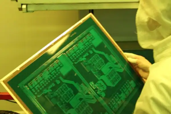
I’ve always found the most fascinating aspect of HDI board manufacturing to be the handling of those unseen details. I remember once visiting a factory and seeing workers inspecting the filling effect of micro-blind vias—that process was like performing microvascular reconstruction surgery on the circuit board. It’s truly difficult to ensure the uniform flow of molten copper in a space with a diameter thinner than a human hair.
Many people may not know that when dealing with high-density interconnects, those seemingly simple steps actually conceal a great deal of expertise. For example, the via filling process, if not properly controlled, may conceal invisible gaps beneath seemingly smooth pads, like planting a time bomb for the entire product.
I’ve paid particular attention to the differences in HDI PCB manufacturing services among different manufacturers. Some manufacturers overemphasize equipment parameters while neglecting the human factor in actual operation. Experienced technicians can judge the filling status by the color of the flux; this accumulated experience is more reliable than machine readings.
One easily overlooked detail regarding the handling of micro-blind vias is the post-drilling cleaning process. If residue isn’t thoroughly removed, poor adhesion during subsequent electroplating can occur. This reminds me of when I was making models; uneven seams, no matter how much paint I applied, couldn’t conceal the flaws.
Recently, I encountered a case where a batch of products experienced signal attenuation during testing. Investigation revealed that the issue stemmed from inadequate wall treatment on a critical layer. Although it passed routine testing, the problem was amplified in high-frequency environments. Such hidden issues often require practical experience to predict.
In fact, when evaluating process quality, the industry should focus more on dynamic indicators, such as stability during continuous production, rather than single-test results. After all, in actual mass production, the production line faces thousands of repetitive operations; even minor fluctuations in any step can be amplified.
I once discussed the alignment accuracy of multilayer boards with an engineer. He used the analogy of threading a needle ten stories high. It requires considering not only the expansion and contraction of each layer but also predicting the displacement during lamination. This dynamic calculation in three-dimensional space is far more complex than two-dimensional drawings.
More and more designs are now pursuing maximum space utilization, which poses new challenges to traditional manufacturing processes. Sometimes, seemingly cutting-edge technical solutions actually require a return to optimizing basic processes, such as improving the flowability of chemicals or adjusting drilling parameters. These details often bring unexpected results.
I believe the key to making good HDI boards lies in understanding the interrelationship between each process. Just like in cooking, the heat and seasoning must work together. Simply pursuing perfection in one aspect may disrupt the overall balance.
Many assume that wireless communication PCBs require expensive high-frequency materials. This guide
When everyone is discussing the hardware race for high-multi-layer Server Motherboard PCBs,
Designing an ECG Monitor PCB is far more complex than it seems.
- Эксперт в области мелко- и среднесерийного производства
- Высокоточное изготовление печатных плат и автоматизированная сборка
- Надежный партнер для электронных проектов OEM/ODM
Часы работы: (пн-сб) с 9:00 до 18:30