
From Novice to Expert: Sharing My Experience in Pin Header PCB Selection
As an electronics enthusiast, I’ve come to understand firsthand the impact of
When I first started in circuit design, I always thought single-sided boards were sufficient. It wasn’t until I was making a small controller and found the wiring unavoidable that I tried double-sided PCB boards. The convenience brought by double-sided routing far exceeded my expectations.
Now, it’s a bit of a shame that many newcomers still habitually prioritize single-sided boards.
I remember a project I did for a smart flowerpot project. They initially planned to use a single-layer PCB, but the sensor power supply and control circuitry were crammed together, causing severe interference. Switching to a double-sided PCB, which layered the power and signal circuitry, immediately solved the problem. This flexibility is something a single-layer PCB simply can’t offer.
Finding a reliable double-sided PCB supplier definitely requires some effort. Once, I went with a cheap option from a small factory, and when I received the boards, I found significant via misalignment. Several pins had solder bridging issues during soldering. The supplier I switched to, although more expensive, had precise via alignment, saving me the trouble of rework.
When choosing a supplier, I particularly value whether they have actual double-sided PCB case studies. Some manufacturers have impressive promotional materials, but their samples clearly show a lack of experience. For example, uneven solder mask thickness or blurred text—these details often reflect their true skill level.
Regarding materials, many double-sided PCB suppliers now recommend high-TG boards. However, for ordinary consumer electronics, there’s no need to blindly pursue high-end materials. The key is to consider the actual application scenario. For example, our outdoor weather station uses ordinary FR4 boards with conformal coating and has been operating stably for several years.
I recently helped a friend review a drone remote controller design and discovered that, in an effort to save money, he forcibly compressed a four-layer board into a double-sided board, resulting in a failed signal integrity test. This made me realize that while double-sided boards are advantageous, their limitations must be recognized. Sometimes, the number of layers is more important than whether it’s single-sided or double-sided.
Actually, there’s a simple way to judge the reliability of a double-sided PCB supplier: see if they dare to disclose their process parameters, such as minimum trace width and via diameter range. Those willing to disclose data are usually more confident in their processes.
At a recent industry exhibition, I discovered that even double-sided boards are now being innovated. Some manufacturers have improved through-hole plating, allowing vias to carry higher currents. This reminded me that when selecting a supplier, I shouldn’t just look at the number of layers but also pay attention to specific process innovations.
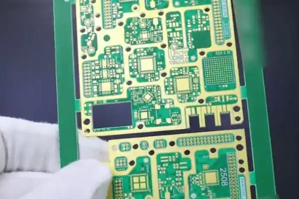
I’ve always found PCB design quite interesting. Many people might think that a double-sided PCB is simply a board with traces on both sides! But anyone who has actually worked on one knows there’s much more to it than that.
I remember being incredibly nervous when I first found a double-sided PCB supplier to make prototypes, fearing that a mistake in any step would ruin the entire batch. Later, I realized that as long as you grasp a few key points, it’s not so scary.
For example, the choice of photoresist. Many people might think any brand will do, but I found that different manufacturers’ photoresists have a significant impact on the final circuit precision. Some are too soft and easily washed away during development, while others are too hard, making removal difficult. Finding the right balance requires repeated experimentation to find the one best suited to your process.
Another important step is post-drilling treatment. Many people overlook cleaning the hole walls, but this step is crucial. If debris remains on the hole walls, subsequent chemical copper plating will cause problems, leading to poor conductivity within the holes. A friend of mine learned this the hard way; several vias failed during testing, requiring rework and wasting a lot of time.
Speaking of double-sided boards, I think the most technically demanding step is hole metallization. Making the insulated hole walls conductive is not as simple as surface-mount wiring. It involves the chemical solution ratio, temperature control, and timing. If any parameter is not adjusted correctly, the entire process can be ruined.
I prefer to check the quality of the electroless copper plating before electroplating. If the thin layer of electroless copper is unevenly deposited, even a thicker layer of electroplating will be useless because the foundation is weak—like building a house with an unstable foundation, no matter how much you decorate it, it will still be a dangerous structure.
Making circuit boards is a bit like cooking; the heat, seasonings, and order all need to be precise. You can’t rush it, you can’t be too slow, you have to follow your instincts—of course, this instinct is built on experience from numerous failures.
Now, whenever I receive a new double-sided PCB prototype, I habitually check the smoothness of the hole walls and then test the conductivity. These details often reflect the supplier’s craftsmanship level. Good suppliers produce boards with uniform hole walls, reliable conductivity, and you can use them with complete peace of mind.
However, even the best craftsmanship needs to be combined with a reasonable design. If the design itself is flawed, even the most skilled craftsman can’t salvage it. Therefore, I believe that learning and practice are equally important and indispensable.
Over the years of making circuit boards, I’ve come to one conclusion—many people overcomplicate double-sided PCBs. Once, I helped a friend modify a simple controller design, and he insisted on covering the top layer with ground wires, resulting in a maze-like wiring layout.
The best thing about double-sided PCBs is their flexibility in space arrangement. I usually separate sensitive signal lines and power supplies on opposite sides, which reduces interference by more than half. I remember once using a regular double-sided PCB for an audio amplifier circuit, initially worried about high noise levels. However, by concentrating the analog components on the bottom layer and moving all the digital switching signals to the top layer, the result was much cleaner than expected.
Choosing the right double-sided PCB supplier is crucial. I once opted for a cheap option from a small factory, and one of their boards had half-unplated vias. Switching to a reliable manufacturer, even though it was more expensive, saved me a lot of trouble. Their manufacturing process directly impacts the feasibility of your design, especially for intricate wiring.
Regarding heat dissipation, I don’t think it’s necessary to deliberately pursue symmetrical distribution. Once, I grouped all the heat-generating chips together, leaving a large copper area on the back and connecting them with multiple vias. The temperature actually dropped by seven or eight degrees compared to a uniformly distributed distribution. The key is to provide a smooth escape path for heat, rather than mechanically distributing it evenly.
Some engineers rely too heavily on automated routing tools. Manual adjustments, while time-consuming, are often crucial to success or failure. Take the classic double-sided PCB routing example—the software showed 100% connectivity, but actual testing revealed clock signal interference. Changing two critical traces to perpendicular intersections immediately resolved the issue.
I hate seeing people densely packed with vias next to solder pads. Modern PCBs are of much higher quality than before. Unless it’s a high-frequency circuit, don’t overthink the “grounding grid” concept; sometimes a simple, direct connection is more reliable.
My recent smart socket project is a case in point. I initially planned to use a four-layer board, but later discovered that widening the power path and rationally layering signal lines with double-sided boards perfectly met the requirements. This made me realize that proper design is more important than simply stacking layers, since each additional layer significantly increases cost.
If you’re new to PCB design, try manually soldering a few simple double-sided boards to get a feel for current flow. This experience is more direct than any tutorial; after all, circuits are connected, not just drawn.
I’ve recently noticed an interesting phenomenon: many people discussing PCB design tend to favor elaborate, multi-layered boards, as if more layers equate to higher technical sophistication. However, in my experience, the most skillful designs often showcase the most basic double-sided PCBs. This seemingly simple structure actually embodies considerable design wisdom, especially when balancing cost and performance.
Last year, while helping a friend design a smart home controller, we experimented with a four-layer board. We later discovered that switching to a double-sided board and rearranging the layout yielded similar results, but at nearly 40% lower cost. This made me realize that the key to double-sided design lies in cleverly utilizing the routing space on both sides. Some designers habitually fill the entire back with ground lines, but leaving appropriate signal channels can actually reduce the number of vias.
Regarding the selection criteria for double-sided PCB suppliers, I believe price shouldn’t be the sole factor. Once, a supplier offered a very attractive price, but the delivered board had substrate delamination issues. It turned out they used substandard copper-clad laminate. Now, I pay particular attention to the supplier’s board material sourcing, such as whether they use high-Tg FR-4 material. While these details may not be visible on the quotation, they directly impact the reliability of the finished product.
Many manufacturers are now pushing automated production, but I’ve found that the real factor affecting double-sided PCB quality is still the manual inspection process. During a factory visit, I noticed experienced workers using strong light to inspect the uniformity of copper plating in through-holes. This experience-based quality control method is more practical than some fancy testing equipment. After all, PCB manufacturing is a highly practical process, and over-reliance on automation can lead to the loss of these valuable experiential judgments.
Regarding the future development direction of double-sided PCBs, I believe that instead of pursuing a stacking of technical parameters, it’s better to consider how to improve the versatility of the design. For example, many IoT devices now need to be compatible with multiple communication modules. If standardized interface designs can be achieved at the double-sided PCB level, the development cycle can be significantly shortened. This design approach is more practically valuable than simply increasing the number of layers.
When choosing partners, I value the smoothness of technical communication. A good double-sided PCB supplier should be able to understand the designer’s intentions and offer constructive suggestions. I once met a manufacturer whose engineers proactively suggested adjusting the solder mask opening size, which indeed solved the bridging problem during soldering. This kind of practical, experience-based technical support is more meaningful than empty talk about intelligent manufacturing.
Ultimately, the charm of double-sided PCBs lies in their balance. Unlike single-sided PCBs, they are not limited by wiring density, and unlike multilayer PCBs, they are not prohibitively expensive. In many consumer electronics fields, this just-right level of complexity best reflects the wisdom of engineering design.
I remember when I first encountered PCB design, I always found those densely packed lines incredibly mysterious. Later, I gradually realized that what truly affects the stability of a board is often not advanced theory, but the way basic details are handled. For example, the 0.15mm trace width and spacing issue often mentioned by double-sided PCB suppliers is often thought to be just a numerical parameter.
I’ve seen many engineers push trace widths to their limits to save space, resulting in open circuits or short circuits during mass production. In fact, 0.15mm is more like a safety margin—like maintaining a safe following distance when driving. Once, when I was designing a board and needed to control costs, I tried reducing the spacing of some non-critical signals to around 0.1mm. The result was no problem in the sample stage, but the yield rate dropped to below 80% in small-batch production. Later I realized that processing errors in double-sided PCB boards accumulate in the trace spacing, so sufficient allowance must be left.
When it comes to metallized vias, many people focus on the hole diameter but easily overlook the hole ring width. During one test, I discovered that vias occasionally broke; upon disassembly, I found that the hole ring width was insufficient, resulting in weak copper adhesion. Afterward, I made it a habit to always indicate that the minimum hole ring width should not be less than 0.15mm during DFM inspections. This seemingly insignificant detail directly affects the mechanical strength of the entire board.
Regarding surface treatment choices, I actually think it’s unnecessary to pursue the latest processes; ordinary lead-free tin plating is sufficient for most scenarios. In a previous project, I chose immersion gold for a “high-end look,” but the cost doubled, and the actual soldering effect didn’t improve significantly. Instead, the brittleness of the immersion gold layer caused several micro-cracks during transportation.
The copper plating method is also worth discussing. Since double-sided boards don’t have a completely flat ground plane, many people try to maximize the copper plating area. However, large-area copper plating can easily cause thermal stress concentration, potentially leading to board warping. I now prefer using a grid-like copper plating, which ensures grounding while allowing for expansion and contraction.
I recently encountered a strange problem while modifying a motor driver board: interference consistently appeared near the power module. Repeated layout adjustments failed to resolve the issue. Later, I focused on the solder mask layer and discovered uneven thickness of the green ink, causing localized capacitance changes. After readjusting the ink printing parameters, the problem disappeared. This made me realize that each layer on a PCB is an interconnected system.
The most interesting aspect of designing double-sided PCBs lies in the need to adhere to physical laws while simultaneously requiring practical wisdom. Sometimes, perfect solutions from textbooks fail in actual production, while seemingly rudimentary methods can solve tricky problems. This balance can only be truly mastered after experiencing a few pitfalls.
Every time I see those exquisite double-sided circuit boards, I’m reminded of my first attempt at hand soldering. Back then, I thought that as long as the components were placed correctly, it would work properly, only to find that it wasn’t that simple.
Choosing a reliable double-sided PCB supplier is more important than the technology itself. Once, to save costs, I went to a small workshop, only to find burrs on the solder pad edges on the boards. Later, I discovered that this was due to shoddy workmanship in the electroplating process, resulting in uneven copper layers. These kinds of details often only become apparent during soldering. For example, some unscrupulous manufacturers use recycled copper or reduce current density, resulting in a copper layer thickness that falls below the standard requirement of 18 micrometers. Uneven heat conduction during soldering directly leads to poor solder joints. Even more problematic is that this defect is easily misjudged as normal in AOI (Automated Optical Inspection) and can only be accurately detected using an X-ray fluorescence thickness gauge.
Many people easily overlook the importance of the testing process. I remember once when debugging a board, it kept inexplicably restarting, and after much troubleshooting, I discovered that there were tiny cracks inside the vias. These problems are completely invisible to the naked eye and require professional continuity testing equipment. Therefore, I now prefer to spend more money to perform full inspection. Especially when the board uses high-frequency signals, via cracks can cause impedance abrupt changes. For example, a transmission line designed for 50 ohms might suddenly spike to 80 ohms, causing signal reflection. Once, using a TDR (Time Domain Reflectometer), I found that a seemingly intact via was actually equivalent to a series inductor at 3GHz, causing ringing on the rising edge.
Electroplating quality directly determines the lifespan of a PCB. I previously used a double-sided PCB from a company claiming military-grade quality, but during high and low temperature cycling tests, the solder pads delaminated. The analysis report later showed that the unstable electroplating solution formula led to decreased adhesion. This hidden problem is more dangerous than obvious open or short circuits. In fact, if the copper cyanide content fluctuates by more than 5% during electroplating, lattice defects will form in the copper layer. On one occasion, disassembling a faulty board revealed that after 200 cycles from -40℃ to 125℃, the peel strength between the solder pads and the substrate dropped from an initial 1.5 N/mm to 0.3 N/mm, far below the IPC standard threshold of 0.8 N/mm.
Now, when choosing suppliers, I pay special attention to their quality control processes, such as whether they perform microsection analysis and regular solderability testing. These seemingly tedious steps can actually help avoid many pitfalls. After all, PCBs are not like software that can be patched; once problems are discovered after mass production, the losses are too great. For example, reputable manufacturers will conduct atomic absorption spectrometry testing of the electroplating bath monthly to ensure that the copper ion concentration is maintained within the process window of 22-28 g/L. During a visit to a supplier’s laboratory, I saw them using a scanning electron microscope to observe microsections. They could clearly see the serrated structure at the interface between the copper layer and the substrate. This mechanical interlocking effect is the fundamental guarantee of reliability.
Sometimes, hardware development feels like walking a tightrope. Every step can be a potential disaster. From substrate selection to surface treatment, any oversight can cause the entire project to collapse. Therefore, I now prefer to spend time on early-stage supplier evaluation, which is far more efficient than later debugging. For example, the TG value of a standard FR-4 substrate can drop from 140°C to 110°C in humid environments, while high-frequency boards like the Rogers 4350B maintain a stable dielectric constant of 3.48. In one project, the use of inferior substrates led to a 15% change in inter-board capacitance in the high-temperature, high-humidity environment of the South China Sea, causing a surge in the bit error rate of the entire communication module.
Recently, I tried a new supplier that surprised me. They even retain samples of each batch of boards for accelerated aging tests. Although the price is a bit high, this meticulous attitude is reassuring. After all, nobody wants a product to fail after only six months, right? Their aging tests include 1000 hours of 85°C/85%RH temperature and humidity bias testing, and 200 rapid temperature transitions between -55°C and 125°C in thermal shock testing. One batch of samples showed micro-cracks in the solder resist ink after testing. They immediately adjusted the UV curing process, extending the pre-baking time from 45 minutes to 70 minutes.
Ultimately, double-sided PCBs, seemingly simple, are actually full of complexities. Simply connecting the circuits is far from enough; long-term reliability must also be considered. This is probably why hardware engineers are always grappling with various details.
I’ve always found choosing a double-sided PCB supplier quite interesting. Many people immediately ask about price, but what they should really focus on is the materials they use. I’ve seen many projects run into problems because the wrong substrate was chosen. For example, some factories use unknown materials to cut costs, causing the copper foil to blister under high temperatures. Good double-sided PCB suppliers will proactively show you material certification reports. One supplier we worked with even sent us videos of bending tests on different materials.
The supply chain is incredibly volatile now. Last year, for an automotive electronics project, the original supplier suddenly announced a three-month supply disruption for a key material. Fortunately, we had prepared a backup plan and found a local double-sided PCB manufacturer that kept a stock of Shengyi and Taiguang substrates in their warehouse. This is when you truly see a supplier’s strength—not by how cheap they are when things are going smoothly, but by their ability to weather storms.
Actually, the technical barrier to entry for double-sided PCBs is higher than many people imagine. I was quite surprised when I visited a factory and saw them using a 2D measuring instrument to check the precision of hole positions—it turns out that even the copper plating thickness of a qualified double-sided PCB needs to be controlled in different areas. Later, when we developed our own smart home products, we paid special attention to this.
Many people think double-sided PCBs are basic and don’t require much attention—this idea is quite dangerous. I’ve worked on medical device projects; even with double-sided PCBs, those used in electrocardiographs need to undergo disinfectant resistance testing; while boards for industrial controllers must pass a seven-day high and low temperature cycle test. These details are completely invisible from the price list.
Recently, the development of flexible double-sided PCBs has changed my perspective. I used to think it was a high-end product until a supplier showed us an ultra-thin double-sided PCB used in wearable devices—it could maintain conductivity reliability even under repeated bending. That’s when I realized that the innovation potential of double-sided PCBs is much greater than I imagined.
Ultimately, choosing a supplier is like choosing a marriage partner—focusing solely on the dowry will definitely lead to losses. You need to see if they’re willing to work through the night with you to revise designs when you encounter difficulties; whether they make excuses or directly adjust the production line when you need urgent prototyping; even whether their engineers ask “What’s the budget?” or “What’s the application scenario?” when they answer the phone. These details determine how far the cooperation can go.
I’ve always found choosing a double-sided PCB supplier quite interesting. When I first started in electronic design, I always thought you could just find any manufacturer, but after a few mistakes, I understood the intricacies. Once, I designed a small device with a wireless module, and because the substrate material provided by the supplier was unstable, the signal was intermittent, and it took me half a month to find the root cause.
The advantage of double-sided design is that it provides more breathing space for circuit layout, unlike single-layer boards that require all traces to be crammed onto one side. However, this also means higher requirements for manufacturing processes, especially the quality of vias, which directly affects the reliability of the entire board. I’ve seen many beginners choose cheap double-sided PCBs to save costs, only to have vias detach during soldering, rendering the entire batch unusable.
Now, I’ve developed a tacit understanding with my long-term double-sided PCB supplier. They know I have stringent requirements for substrate flatness and proactively send material testing reports before each production run. This trust isn’t built overnight; after all, PCB quality directly determines product lifespan.
Recently, when I tried using thick copper foil in a motor drive board design, the supplier specifically reminded me to adjust the solder mask process to avoid edge coverage issues caused by thick copper. This kind of detailed experience is often more practical than technical parameters; ideal curves on the drawings must always be tested in real-world production.
Actually, there’s a simple way to judge a supplier’s professionalism—see if they proactively discuss your specific application scenario. Excellent suppliers will offer suggestions from the perspectives of heat dissipation and mechanical strength, not just quotes and delivery times. After all, we need not just a cold circuit board, but a stable, functional solution.
Sometimes I feel that choosing a PCB supplier is like finding a fitness coach; it’s not enough to just look at their qualifications—you also need to see if they truly understand your needs. Good collaboration allows design intentions to be accurately realized, while perfunctory cooperation will only turn the later debugging into a nightmare.
As an electronics enthusiast, I’ve come to understand firsthand the impact of
Why is green the universal choice for circuit boards? Behind this seemingly
As a hardware entrepreneur, I often see teams fall into a trap
- Эксперт в области мелко- и среднесерийного производства
- Высокоточное изготовление печатных плат и автоматизированная сборка
- Надежный партнер для электронных проектов OEM/ODM
Часы работы: (пн-сб) с 9:00 до 18:30