
What critical role do data center PCBs play in AI training clusters?
While everyone focuses on the computing power of AI chips, the physical
Whenever I see electronic components neatly and precisely placed on a circuit board, I am reminded of my first encounter with custom PCBs. Many people assume that PCB assembly is a process handled entirely by machines—something you don’t really need to worry about. In reality, there are quite a few nuances worth considering.
When I first started out, I thought that simply sending over the design files was enough. Later, I discovered that component selection has a huge impact on the final result. Once, we chose a somewhat uncommon chip and ran into trouble during soldering; its pin pitch was so tight that standard stencil aperture designs couldn’t ensure an even distribution of solder paste. That batch of boards required multiple rounds of rework before they were even usable. Since then, I’ve paid close attention to how well component package specifications align with the soldering process.
Speaking of soldering, I think the quality of the solder paste is the most overlooked factor. It might look like just a thin layer, but it plays a crucial role. High-quality paste has the right flow characteristics—it keeps components from shifting during placement while ensuring robust solder joints during reflow. I once tried to cut costs by using a cheap paste, and the boards developed cold solder joints in less than six months. Switching to a reputable brand solved the problem for good; it cost a bit more, but it saved me the headache of future repairs.
The era of manual soldering is long gone; most steps are now handled by automated equipment. However, that doesn’t mean you can simply walk away and ignore the process. Details like checking stencil alignment before SMT placement or configuring the reflow oven’s temperature profile often determine the final yield. I’ve seen factories skip these checks to meet a deadline, only to end up scrapping the entire batch—which actually wasted even more time in the long run.
Through-hole components are less common these days, but they remain essential for high-power applications or situations requiring mechanical strength. While the soldering process is simpler than SMT, issues can still arise—like installing a component backward or failing to trim the leads properly. I once overlooked a capacitor’s polarity and installed it the wrong way around; it started smoking the moment I powered it up. So, you have to stay vigilant, even with the simplest steps.
Ultimately, custom PCB assembly isn’t just about handing things off to a machine. Human oversight is required at every stage, from material selection to soldering. Equipment is getting smarter, but human experience and judgment remain vital—after all, we’re the ones using the final product, not the machines.
I’ve seen too many people overcomplicate the idea of custom PCB assembly. In reality, the biggest headaches aren’t usually technical issues—they stem from failing to get the seemingly simple preparatory work right.
Take the Bill of Materials (BOM), for example. Many people think a casual list—like “some resistors and capacitors”—will suffice, but the assembly plant often ends up buying parts with the wrong specifications or components that are completely unusable. You really need to list the manufacturer’s part number clearly for every single component! I learned this the hard way once: I used an internal code for a power management chip instead of the standard model number, and the entire batch of boards had to be reworked.
Silkscreen markings are another thing that’s easily overlooked—people often think, “It’s just some small white text, right?” But have you considered how troublesome it is during repairs if you can’t find the corresponding location markers? I remember a board where the silkscreen was too close to the solder pads; the ink smudged during soldering, and in the end, we had to guess where the components went.
Speaking of component selection—many beginners make the mistake of chasing the newest, most expensive models. But did you know? Sometimes, older models that have been in mass production for years are actually more reliable, offer stable supply, and cost significantly less.
I feel that PCB work tests your attention to detail more than your technical skills—you have to double-check everything, from every field in the BOM to every character on the silkscreen. After all, if a mistake slips through, fixing it later costs many times more!
I always find it amusing when I see articles portraying “Custom PCB Assembly” as something incredibly high-end or mysterious. When you strip it all away, isn’t it just mounting a bunch of parts onto a board according to a blueprint? It’s just that machines have replaced manual labor, offering a bit more precision and speed.
When I first started in this industry, I thought PCBA was a mysterious process. Later, after visiting a few factories, I realized that quality isn’t determined by how advanced the equipment is, but by whether the people doing the work truly care. I once watched a veteran technician inspecting solder joints with a magnifying glass; that level of focus was more reliable than any automated inspection equipment.
Many people associate “custom” with high prices, but that’s not the case at all. There are so many manufacturers in China doing this now, and the competition is fierce. The key is knowing exactly what your requirements are. Some projects do require high-precision equipment, but in many cases, standard processes get the job done just fine—there’s no need to spend extra money. I recall a client who insisted on using state-of-the-art equipment for their prototype boards, only to find the cost was three or four times higher than expected. Later, they switched to a standard manufacturer and got results that worked just as well. It’s like going grocery shopping: if you’re just stir-frying some greens, insisting on organic produce isn’t impossible, but it’s simply unnecessary.
In my opinion, the biggest headache with custom manufacturing isn’t actually the technical side of things. Many beginners stumble right at the file preparation stage. I once received a design file that didn’t even include enough clearance for the manufacturing margins—the factory couldn’t put it on the production line at all. These kinds of basic errors are completely avoidable.
Ultimately, finding a manufacturer for PCBA is a lot like hiring a renovation crew: you need to be clear about your requirements first and then find a reliable partner. Don’t rush to place an order just because the quote looks low.
It always makes me smile when I see novice designers agonizing over component selection in front of their screens. They often think that picking a part with “similar specs” is enough, without realizing the pitfalls waiting down the line. Just last week, a client brought us a custom PCB design, only for us to discover a global shortage of the main control chip; it took a full two months just to gather all the necessary components.
Honestly, the most stress-free way to handle PCBA is to simply hand the Bill of Materials (BOM) over to a reliable manufacturer and let them handle everything. I’ve seen too many people try to manage procurement themselves, only to end up with refurbished parts or counterfeits that ruin the entire batch of boards. Professional assembly houses deal with suppliers constantly; not only do they get better prices than the retail market, but they can also secure inventory for hard-to-find components in advance.
One detail many people overlook is how well the design files match actual production requirements. For instance, if you use a capacitor with a non-standard package size in your layout, the manufacturer might order standard-sized parts by mistake, causing errors on the pick-and-place machine. Having the manufacturer review your design files beforehand can save you a lot of trouble.
Regarding files, I think coordinate files are the most frequently underestimated element; some people don’t even clearly mark the top and bottom sides when exporting them. I once received a board where all the LEDs were mounted backward because the file didn’t distinguish between the top and bottom layers. While we can often spot this through experience, a new operator following the file strictly could easily cause a disaster. Nowadays, any reasonably professional manufacturer offers online review services; when you upload your design files, their system automatically checks component inventory and manufacturing compatibility. This transparent process is far more efficient than the old method of back-and-forth email confirmations—after all, no one wants to wait for a prototype to arrive only to discover a specific resistor is completely unavailable.
Ultimately, the old adage “leave professional tasks to the professionals” holds especially true in electronics manufacturing. You might spend a week comparing prices and sourcing parts to save a few hundred yuan, but the resulting delay to the project schedule could cost tens of thousands—it simply doesn’t add up.
I recently worked on a medical equipment project where the client insisted on using a specific brand of connector; during the wait for materials, the market price tripled. Had they accepted the manufacturer’s recommended alternative earlier, costs could have been controlled, and the delivery time cut in half. Sometimes, fixating on a specific component is unnecessary, as the performance gap with modern alternatives is often negligible.
I recommend communicating closely with the manufacturing team during the PCB design phase. It might seem like a minor detail, but it often determines whether the project can be successfully executed.
After years of working with circuit boards, I’ve found that the biggest headache isn’t the actual design work—it’s finding a reliable assembly house. Early on, I felt most at ease sourcing and delivering all the components myself, since I knew exactly where every part came from. But I eventually realized that wasn’t the best approach.
Once, I specially ordered a batch of unique sensors from abroad, only to find upon arrival that the package size was incompatible with the pick-and-place machine, stalling the entire project for two weeks. That’s when I understood why veteran engineers always advised choosing manufacturers that offer comprehensive services. Their warehouses often stock a wider range of basic components—like resistors, capacitors, and inductors—than you’d imagine, and they frequently update their inventory.
Now, when I need custom PCB assembly, I prefer letting the factory handle the procurement of most standard components. It’s not just about convenience; their bulk purchasing prices are far more cost-effective than buying small quantities ourselves. This is especially important when racing against a deadline—waiting to compare prices and source parts individually can cause significant delays.
Of course, I still insist on sourcing certain core chips myself—specifically critical components like main control chips that require specific firmware. In this scenario, a partial consignment model works particularly well—it ensures control over core components while leveraging the factory’s supply chain strengths to quickly source basic materials. Just remember to verify the component packaging format beforehand; don’t make the kind of rookie mistake I once did.
Ideally, you want to find an assembly partner that is flexible enough to accept consigned materials while also possessing robust material management capabilities. This prevents a single specialized component from stalling the entire project while ensuring efficient supply of standard parts. After all, the worst part of hardware development is waiting for all the materials to arrive; watching a production line sit idle is agonizing.
I’ve always felt that many people misunderstand custom PCB assembly. They assume it’s like buying off-the-rack clothing—just pick a size that’s “close enough” and make it work. In reality, true customization is tailored to your specific needs from the ground up. When our team worked on a smart home project last year, we initially tried cobbling together off-the-shelf modules. We found that the power consumption was slightly off and the stability didn’t meet requirements. It wasn’t until we switched to a fully customized process that we realized the key wasn’t the modules themselves, but how well the various components worked in harmony.
We revised our design files over a dozen times before submission. Some might think, “Isn’t it just a matter of sending the blueprints?” But a proper manufacturing file must account for factors like board thickness, trace width tolerances, and even thermal expansion and contraction during soldering. Once, a grounding point was off by just 0.1 millimeters, causing cold solder joints across the entire batch during high- and low-temperature testing. These kinds of details might never surface with standard products, but in a custom scenario, they can be fatal flaws.
Many people simplify PCBA to just “placing components on a board,” but it’s actually more like a precision-choreographed dance. The placement, orientation, and even heat dissipation paths of every component need to be clearly planned from the start. We once had a client insist on using a substrate made of a special material, only to discover during mass production that it couldn’t withstand the high temperatures of reflow soldering. We switched to a standard material combined with a localized heat dissipation design; not only did costs drop by a third, but performance also became more stable. That experience taught me that customization isn’t about piling on expensive materials—it’s about finding the optimal balance.
What really left an impression on me was an upgrade project for a medical equipment manufacturer. They had been using the same circuit board for eight years and wanted to boost processing speeds without changing the board’s physical dimensions. We redesigned the layout to integrate chips—originally requiring external mounting—directly onto the motherboard, using the freed-up space to add shielding layers. You see, true customization often involves meticulous work in places that aren’t immediately visible.
Ultimately, a good customization service should be like a master tailor crafting a suit: they don’t just measure your dimensions; they also ask about your lifestyle. A startup team recently complained to me, asking why a competitor quoted half our price for the same functionality. I opened their design files and pointed out the corners cut to save costs—details that would ultimately shorten the product’s lifespan by over 30%. Some choices may not show a difference right away, but time reveals the truth.
Whenever I see the densely packed circuit board layouts inside miniature devices, I wonder: are we focusing too much on technical specifications while ignoring the actual needs of real-world applications? A recent project helping a friend modify an outdoor weather station gave me some new insights.
Their team had originally crammed all passive components into a space smaller than a fingernail in pursuit of extreme miniaturization; consequently, the device suffered frequent signal drift in mountainous areas with significant temperature fluctuations. We later redesigned the custom PCB assembly, swapping some key resistors and capacitors for standard-sized components. Although the volume increased by 15%, the device ran continuously for six months without a single issue. This made me realize that in certain applications, reliability matters more than miniaturization.
Many PCBA designs today blindly chase the technological cutting edge while ignoring the user’s actual operating environment. For instance, while embedded components save space, they are nearly impossible to replace individually during repairs; if a single link fails, the entire board often has to be scrapped. I’ve seen plenty of industrial equipment adopt overly compact designs for the sake of a so-called “tech upgrade,” only to end up with maintenance costs that exceed the price of the equipment itself.
In reality, a good circuit board design should allow for flexibility, much like building with blocks. Last week, while debugging an IoT terminal, the manufacturer initially wanted to mount all chips directly onto the baseboard. We insisted on retaining modular interfaces instead; the client later reported that this design allowed for rapid sensor module replacement in the field, significantly simplifying maintenance.
As for future trends, I believe that rather than obsessively pursuing technological breakthroughs, we should focus more on how different manufacturing processes can work together effectively. Additive manufacturing, for example, can certainly achieve finer circuitry, yet traditional etching processes still hold a cost advantage for mass production. The key is to select the right technology mix based on product positioning, rather than being led astray by so-called trendy concepts.
I recently encountered an interesting case: a medical device manufacturer actually reverted from surface-mount chips to through-hole packaging for their second-generation product. Although the thickness increased by 2 millimeters, the yield rate improved by over 30%. Such design adjustments, driven by real-world feedback, are far more compelling than any theoretical analysis.
Ultimately, a circuit board is the product’s backbone, not a fashion runway. A truly excellent design should stand the test of time, even if it means sacrificing certain “cool-looking” technical specifications. After all, users want stable, reliable performance, not perfect data from a laboratory setting.
I’ve seen far too many teams stumble when it comes to PCBA. They often assume that simply handing the design files over to the factory is enough to get the job done. In reality, there are several critical hurdles to clear between the circuit board design and a fully functional product. I recall a time when our team was rushing to launch a new product; the designer had created a highly complex board, but the first batch of samples wouldn’t even power up. Upon inspection, we discovered that a specific chip required unique soldering temperature parameters—standards that standard reflow soldering processes simply couldn’t meet.
For instance, certain BGA-packaged chips require precise preheating profiles and peak temperature control; a temperature deviation of more than 5°C can result in cold solder joints or internal chip damage. Such nuances are difficult to fully capture in design drawings alone; they often require dynamic adjustments based on a combination of component datasheets and actual manufacturing capabilities.
This experience taught me a valuable lesson: in electronics manufacturing, making assumptions is dangerous. Parameters that seem clearly defined on paper can play out very differently on the actual production line. We subsequently adjusted our strategy: for every new board, we send an engineer to the factory to oversee production—watching exactly how components are placed and how the boards pass through the reflow oven. This kind of on-site communication is far more effective than endless back-and-forth emails. During line inspections, we often find that stencil aperture ratios need fine-tuning; for example, using standard apertures for 0402-package capacitors often causes solder beading, so experienced engineers might recommend a trapezoidal aperture design. These detailed optimizations can boost the first-pass yield by over 15%.
When selecting manufacturing partners now, I prioritize adaptability. I recall a time when we faced a sudden material shortage; the partner’s engineers called in the middle of the night to discuss alternatives. They not only proposed three substitute components but also recalculated the thermal dissipation parameters. That proactive problem-solving attitude is what truly adds value. For instance, when the lead time for a specific MCU stretched to six months, they simultaneously evaluated pin-compatible alternatives and worked overnight to produce and test validation boards, ensuring full functionality after the firmware migration. This level of deep collaboration shortened our project timeline by nearly three weeks.
Ultimately, custom PCB assembly isn’t just about placing an order; it’s a journey of collaboratively refining a product. A great manufacturer helps ground your ambitious ideas in reality while steering you clear of hidden pitfalls. I gained a deep appreciation for this while working on a smart home project: seeing the PCB factory owner personally squatting by the production line to adjust solder paste thickness told me we had found the right partner. They even maintained a defect database, visualizing data on PCB substrate materials versus solder paste ratios to provide early warnings about risks like ion migration or board delamination.
A truly reliable manufacturer treats every detail as a work of art rather than simply fulfilling an order mechanically. For instance, when assembling medical device motherboards, they proactively add a thickness inspection step after conformal coating and use X-rays to spot-check BGA solder joint fullness; these requirements—which go beyond standard protocols—often prevent major quality failures after the product hits the market.
I recently encountered an interesting scenario while working on a medical device project for a friend: the circuit board had to fit into a space the size of a matchbox while ensuring a ten-year service life. This extreme miniaturization forced me to rethink the logic behind flexible PCB material selection. Material biocompatibility becomes the primary consideration—especially for implantable devices—requiring the use of USP Class VI certified polyimide substrates, a choice that directly dictates the subsequent manufacturing process.
Conventionally, people assume liquid photoimageable (LPI) solder masks are sufficient, right? However, actual testing revealed that coverlay materials perform quite differently in areas subject to repeated bending. After comparing the flexural endurance of three different materials, we found that rolled-annealed (RA) copper truly excels in dynamic applications; its grain structure withstands significantly more bending cycles without cracking. For example, in tests simulating the 200 daily bends experienced by a wearable device, RA copper demonstrated a fatigue life more than three times that of electro-deposited (ED) copper—a disparity that becomes particularly pronounced during durability tests reaching the million-cycle mark.
Regarding quality control, I want to highlight the value of X-ray inspection. Last week, we examined a BGA chip that had been returned for rework; it appeared flawless on the surface, but X-ray imaging revealed internal solder joint fractures—defects that would have been impossible to detect via the naked eye or standard AOI. This is especially critical when solder ball diameters are under 0.3mm, as X-rays clearly reveal the morphology of intermetallic compounds at the solder interface, which is vital for assessing long-term reliability.
Speaking of AOI systems, while high-resolution cameras capture a wealth of detail, they still have blind spots when inspecting the micro-blind via structures found in miniaturized designs. We recently experimented with combining AOI and X-ray inspection and discovered they effectively complement each other, covering inspection gaps by simultaneously identifying surface-mount issues and internal connection quality. For instance, when inspecting connectors with a 0.2mm pitch, AOI handles pin coplanarity checks, while X-ray imaging allows us to verify solder fill rates. In fact, the aspect of flexible circuit boards most easily overlooked is the choice of lamination process. Although adhesive-free laminates come at a higher cost, they offer superior thickness control—making them particularly suitable for wearable device projects that demand strict dimensional precision. Take the battery connection area of a smart wristband, for instance: adhesive-free lamination keeps the total thickness under 0.1mm and ensures a more stable dielectric constant, a factor that is critical for high-frequency signal transmission.
During the acceptance inspection of a batch of rigid-flex boards, we observed a curious phenomenon: boards from the same batch performed very differently in high-temperature environments. Traceability analysis revealed that the inconsistency stemmed from varying rolling directions of the rolled copper—a discovery that highlighted the importance of material traceability for me. We now require suppliers to specify the rolling direction on material certificates and consider the alignment between the bending direction and the material’s grain (rolling direction) during the design phase.
When handling custom orders now, I pay closer attention to specific application parameters—such as bending frequency and the range of ambient temperature and humidity fluctuations. These seemingly mundane factors often dictate the choice of process more than standard technical specifications do. For example, in automotive electronics, one must account not only for temperature cycling between -40°C and 125°C but also for potential fretting wear on cables caused by vibration.
I recall an instance where we skipped certain inspection steps to meet a tight deadline; the resulting hidden defects in the initial batch actually caused even greater delays. That lesson taught me that there are no shortcuts in quality control. We now mandate cross-sectional analysis for bending zones and verify the bond strength between the coverlay and copper foil, even for the simplest single-sided flexible boards.
Clients sometimes ask why flexible boards are priced so much higher than standard PCBs. In reality, the cost differences—spanning everything from material selection to specialized testing—are far more complex than they appear on the surface. It is akin to the difference between medical-grade silicone and ordinary plastic: they may look similar, but their properties are worlds apart. Medical-grade flexible boards, for instance, must be manufactured entirely in cleanroom environments, and samples from every batch must be retained for accelerated aging tests.
Lately, I have come to realize that excellent process design isn’t about piling on the most advanced technologies; it is about finding the optimal balance for the specific application. It is much like cooking—simply doubling the amount of every seasoning won’t necessarily make a dish tastier; the key lies in the right combination of ingredients. Take the selection of materials for fitness tracking devices, for example: we ultimately chose a mid-range, modified polyester film. It struck the perfect balance between sweat resistance and flexibility—a far more practical choice than blindly chasing high-spec materials.
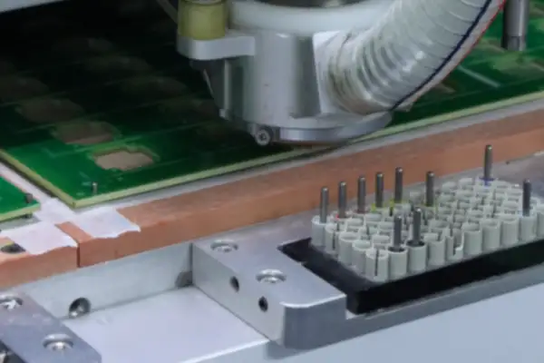
I’ve seen far too many people stumble when it comes to custom PCB assembly. They often assume that simply handing the design files over to the factory is enough, only to find that the first batch of boards comes back with lifted pads or components that don’t align with the holes. Dealing with that kind of headache can set you back weeks.
The root cause usually lies in the design phase. Many designers focus solely on making the routing look neat without considering whether the board is actually manufacturable. A friend of mine was developing a smart home controller; it passed all functional tests, but the factory rejected it immediately because the spacing between chip pads was too tight for the pick-and-place machine to align accurately.
That’s why DFM (Design for Manufacturability) checks are so crucial. It’s not about finding faults in your circuitry, but rather evaluating your design from a manufacturing perspective to see if it might cause issues on the production line. For instance, packing components too close to the board edge can lead to cracking during depanelization, while poorly placed thermal vias can cause heat buildup and warping during reflow soldering. These seemingly minor details directly determine whether your project can successfully move into mass production.
Many PCB manufacturers now integrate DFM analysis directly into their quoting systems. You get alerts about potential risks as soon as you upload your Gerber files—far better than discovering issues after a failed prototype run. Last week, I was modifying a drone flight controller board for a studio; the online quote page flagged two areas where the solder mask bridges were too narrow. Adjusting the trace widths actually ended up lowering the cost by 3%.
The truly stress-free approach is to consider manufacturing requirements from the moment you draw the very first trace. When selecting components, don’t just look at specifications; consider whether the package is readily available and compatible with pick-and-place machines. When laying out the board, leave sufficient manufacturing margins and avoid hiding test points beneath heatsinks. This upfront effort might seem time-consuming, but it paves the way for smooth mass production later on.
A recent case illustrates this point perfectly: a team developing a motherboard for medical equipment packed the routing extremely densely out of concern for signal interference. The factory eventually reported that this design required more expensive materials to ensure a high yield, which would have doubled the mass production costs. Later, they optimized the layout and added grounding shields around critical signal lines, achieving the same performance using standard board materials.
Ultimately, PCB design and manufacturing are inextricably linked. A good engineer cannot simply live within simulation software; they need to visit the production line regularly to see how circuit boards are actually made. Projects that succeed on the first attempt are invariably the result of close, ongoing communication between the design and manufacturing teams.
Sometimes, a simple adjustment to component orientation can boost SMT placement efficiency by 20%, or moving test points from the top to the bottom of the board can eliminate an entire inspection step. These are insights you simply cannot gain from textbooks alone.
I’ve made it a habit to send my Gerber files to a trusted process engineer for a quick review before finalizing any design iteration. Their suggestions—based on manufacturing realities—often reveal issues I would never have spotted myself. This kind of cross-disciplinary exchange is more effective than any design guideline.
After all, no one wants a carefully crafted design to get stuck at the final hurdle, right?
While everyone focuses on the computing power of AI chips, the physical
Many engineers misunderstand buried via PCBs, often viewing them as a hallmark
When it comes to heat dissipation, do aluminum-based boards immediately come to
- Эксперт в области мелко- и среднесерийного производства
- Высокоточное изготовление печатных плат и автоматизированная сборка
- Надежный партнер для электронных проектов OEM/ODM
Часы работы: (пн-сб) с 9:00 до 18:30