
RF Communication PCB: How to Avoid Expensive Material Traps and Achieve Reliable High‑Frequency Performance
High-frequency PCB design is not metaphysics; senior engineers share real experience. In
I have always felt that many people’s understanding of high-frequency PCB is a bit off. When people mention materials like mmWave PCB or Rogers PCB, they always like to talk about those scary technical parameters and market forecast figures. Actually, it’s not that mysterious. I have met many engineers. When they get a millimeter wave project, their first reaction is to read the data sheets of those top-grade boards and then start to worry about the cost issue.
This idea was flawed from the beginning. The real question is whether we really need “high frequency” for the sake of “high frequency”. I have seen a team that makes smart home sensors. They insisted on using advanced high-frequency PCB materials to make a simple 24GHz ranging module. As a result, the cost was 40% higher than competing products, and the project ended up being scrapped. What they didn’t understand was that in that application scenario, there was no need for such extreme performance stability, which was much more important than the theoretical loss reduction.
So my view is don’t let those grand predictions for 2025 lead you away. The market is indeed growing, but the driving force for growth is not a parameter competition but finding the right scenario. For example, the so-called “millimeter wave” sensors used in many industrial Internet of Things applications actually have far less stringent requirements on board materials than everyone imagines. Sometimes the use of well-designed ordinary FR4 materials combined with reasonable structural design can fully perform the job and reduce the cost by a large margin.
Of course I’m not saying that high-end materials are useless. When you really want to make 77GHz automotive radar or high-end communication equipment, the value of materials like Rogers PCB becomes apparent. Their stability is really good, and the dielectric constant changes very little with temperature and frequency, which is crucial to ensuring long-term reliable operation of the system. But the key is to figure out whether every extra penny you spend can really improve the performance or reliability of the end product.
I think there is a bad trend in the industry right now, which is that millimeter wave products cannot be made without using the most advanced boards. On the contrary, this has caused many innovative applications with great potential to be stuck due to cost issues.
In the final analysis, PCB is a carrier for realizing functions. It should serve the product logic rather than letting the product make do with the board.
What I am more optimistic about is the layered design idea of mixing different grades of boards or even integrating different materials on the same board according to the actual performance requirements of different parts of the circuit. This certainly requires higher design and process requirements but may be a pragmatic direction to balance performance and cost in the future.
In short, don’t think of high-frequency PCB design as a purely technical multiple-choice question. It is more like a business judgment. You have to clearly know where the core value of your product is and then allocate resources for this value instead of blindly pursuing high-performance indicators on paper. It doesn’t make much sense.
I recently chatted with some engineers who are working on high-frequency projects, and I found that everyone generally has a misunderstanding, that is, as long as they use boards like Rogers, everything will be fine. In fact, things are not that simple. Yes, when processing millimeter wave signals, the loss factor of the plate itself is crucial. This is the basis. But what really determines success or failure are often the overlooked details, such as processing accuracy.
Take a simple microstrip line as an example. When you work in the millimeter waveband, the wavelength of the signal is already as short as a few millimeters. At this time, even a few micron burrs on the edge of the conduction band or slight unevenness in the thickness of the dielectric layer will cause unexpected reflection and radiation losses. These additional losses introduced by processing add up to considerable amounts.
I have seen a case where the simulation performance during design was very beautiful. Top-grade low-loss boards were used, and the theoretical loss value was extremely low. However, in the actual board test, the performance was compromised. After repeated investigations, it was discovered that the problem was with the solder mask ink. The performance of ordinary solder resist materials is not stable in the millimeter wave frequency band, and covering the transmission line will introduce considerable parasitic capacitance and additional dielectric loss.
So my point of view is that in high-frequency PCB design, material selection is only the first step. Plates like Rogers do provide an excellent starting point, reducing the loss of the base material itself. But if you don’t take the processing technology, surface treatment, and even the pad design of component soldering into consideration, the final effect may not meet expectations. It’s like if you use the best ingredients but let a chef who is unfamiliar with the cooking methods cook it, the taste of the dish will still be wrong.
We have to change our thinking: from simply pursuing “low-loss boards” to building a “low-loss system”. This means that your design must be closely tied to the manufacturing process. You need to communicate with the PCB factory in depth about the limits of their processing capabilities, such as what is the minimum line width and line spacing they can stably control, how much surface roughness their copper plating process can achieve, and whether they have ever processed boards with similar frequencies.
Sometimes, in order to accommodate processing capabilities, the design rules are slightly adjusted, such as slightly widening the line width in exchange for better etching consistency. The final improvement in system performance is much greater than simply changing to a more expensive plate material.
In short, don’t bet all your money on materials.
A good high-frequency PCB is an indispensable product of the perfect combination of design, materials and technology.
Recently, I discovered a very interesting phenomenon while chatting with some friends who make hardware: everyone seems to be rushing to make so-called high-frequency boards. Open various technical forums or industry news, and you will see the words “mmWave PCB” and “high Frequency PCB” almost every day. But to be honest, I have a slightly different opinion.
I think the entire industry is a little too superstitious about materials and craftsmanship. When talking about making millimeter wave boards, many people’s first reaction is that they must use high-end boards like Rogers. It seems that using PTFE or Rogers materials will automatically solve the performance problem. This is actually a big misunderstanding.
I have seen many projects where the initial design ideas were skewed and a large amount of budget and time were spent on material procurement. However, when the board came back and the signal was tested, it was still a mess. What’s the problem? Many times it is because the foundation of the design itself is not laid properly, such as unreasonable wiring layout, failure to control impedance, or insufficient understanding of the process capabilities of the processing plant. Even if you use the best Rogers PCB, if the processing factory has insufficient experience in handling high-frequency circuits and the etching accuracy is not enough, the final effect may not be as good as using ordinary boards but with a more carefully designed solution.
What really determines the success or failure of a high-frequency PCB is the seemingly inconspicuous basic work.
I participated in a vehicle radar project team last year. At first, we were obsessed with specifying a certain expensive imported base material. Later, we changed our mind and spent time to make the simulation model of the antenna array very detailed, even taking into account the impact of the connector pads. Then we found a domestic processing factory that we have cooperated with for many years. Although they have not used such high-end materials, they have a thorough understanding of our design intentions and are very patient in adjusting the process parameters. The cost of the final board dropped a lot but the performance test results exceeded expectations.
This experience makes me think that by around 2025, this industry may undergo a very important change: everyone will no longer blindly pursue “top materials” but will pay more attention to “system-level design and manufacturing collaboration capabilities.” Whoever can seamlessly integrate the three links of design, material selection, and processing technology can truly make stable and reliable high-frequency products.
Many discussions now focus on the technical specifications of the 77GHz or higher frequency band, which is of course important, but I think the focus of competition in the next stage will shift to how to achieve large-scale, consistent high-quality manufacturing. After all, no matter how good the laboratory sample is, it will lose its commercial value if it cannot be stably produced in batches. For those who actually make products, the actual significance of a one percentage point improvement in yield may be much greater than a reduction in the loss tangent value of a certain material by a few tenths.
So my point is don’t be led by those gorgeous parameters and material models.
Calm down and do a solid job in basic skills. Understand what your circuit needs. Understand what your factory can do well. On this basis, choose the most suitable rather than the most expensive material route. This may be a more practical way to deal with future high-frequency PCB challenges.
I recently chatted with some friends who make high-frequency circuits and found that when everyone mentioned millimeter wave design, their first reaction was to look for Rogers plates. This is of course true. Materials such as Rogers 4350B do have a good reputation in the industry, but I feel that this line of thinking is a bit biased, as if things cannot be made well without it. In fact, many projects focus on the highest-end materials from the very beginning, but in the end the cost cannot be realized at all.
My experience is that what really determines whether your circuit can run is often not the accuracy of the nominal Dk value of the board itself, but the ability to control the loss of your entire link. The bulk of the loss here is often not the medium itself, but the conductor loss. Many people spend a lot of money to buy low-loss board rolls. However, in the PCB processing factory, due to the mismatch of copper foil processing technology or wrong lamination parameters, the insertion loss of the final board is measured, which is far from expected.
This has to mention a key thing: the surface roughness of the copper foil. For millimeter wave frequency bands, such as 77GHz, signals are transmitted in a very thin layer on the surface of the conductor. This phenomenon is called the “skin effect.” At this time, if the surface of the copper foil is rugged, the signal will be like climbing over mountains, and the energy loss will be very large. No matter how good the low-loss substrate you choose is, it will be useless. Therefore, more and more high-frequency PCB designs now begin to specify HVLP (ultra-low profile) copper foil, or even rolled copper. Although the cost of rolled copper is much higher than that of commonly used electrolytic copper foil, its surface is extremely smooth and flat, and its conductor loss advantage at high frequencies is very obvious.
Of course, I am not saying that media materials are not important. The Df value, which is the loss tangent, must be as low as possible. But in actual projects, you have to calculate the general ledger. For a Sub-6GHz 5G antenna board, if it is extremely cost-sensitive and the performance requirements are not the limit, sometimes it is not impossible to use some improved FR-4 materials. Its Df may be between 0.008 and 0.012. Although it is not as good as the Rogers series, which is often a few tenths, but as long as your traces are not long and the design is appropriate, it can fully meet the link budget of many consumer-grade products. Blindly pursuing the ultimate low Df will cause your BOM cost to skyrocket.
The most pragmatic approach I’ve seen is mixed pressure design. This is actually a very smart idea: only spend money where you really need it. For example, a 5G small base station motherboard integrates radio frequency front-end, digital processing and power management. You can use a small piece of Rogers 5880 or similar high-frequency materials to make the radio frequency antenna and key millimeter-wave feeder parts, while the digital circuit and power supply parts use ordinary FR-4. They are made together through the lamination process of multi-layer boards.
This not only ensures the low-loss characteristics of the core radio frequency channel, but also controls the overall cost from being too exaggerated. After all, the entire board is made of Rogers materials. It is very common for the cost to triple or five times, which is simply unrealistic for products that require large-scale commercial use.
So my opinion is that when designing high-frequency PCB or mmWave PCB, don’t just focus on the parameters in the material manual. It is a system engineering: you have to comprehensively consider your frequency, trace length, tolerance for loss, process capabilities of the processing plant, and the most realistic project budget.
From the design end, it is necessary to think about how to use the appropriate material combination, match the correct copper foil type and processing requirements, to achieve the best balance between performance and cost. This is where the real test of engineering ability is far more complex and valuable than simply specifying a “best” material.
Every time I see someone talking about millimeter wave PCB design in such a mysterious way, I want to laugh. It seems like you have to use some exorbitantly expensive materials to do it, but it’s actually not that complicated. After working on many projects, I found that what really affects performance is often some basic choices, such as boards.
Many people stare at Rogers boards as soon as they get started, thinking that the more expensive ones are better. In fact, ordinary FR-4 can also be used very well in many situations. The key lies in how you deal with the problem of its dielectric constant changing with frequency. I have done a comparison test. Using a suitable FR-4 laminate design in a certain frequency band, the performance is not much worse than those high-end boards.
When it comes to lamination, I find that many people have a too rigid understanding of the middle layers of L2, L3, and L4. Why do we have to follow what is in the textbook? Sometimes placing the power plane on L3 and the second ground plane on L4 can better control the impedance. I have tried adding a very thin dielectric layer between L2 and the top layer to reduce loss, and the effect is much better than simply pursuing surface roughness.
The most easily overlooked aspect in high-frequency PCB design is processing accuracy. It doesn’t matter how beautiful the drawings are, it’s all useless if the factory can’t make it or the deviation is too big. After working with several factories for a long time, I learned that there are only so many tolerances they can stably control, and you have to take them into consideration during the design stage.
There are also so-called “advanced materials”, such as certain specially treated copper foils, which are highly publicized. But after actual testing, I found that in many cases the performance improvement is not obvious and the cost doubles. It would be more practical to spend this budget on optimizing wiring and reducing vias.
I have seen many engineers become obsessed with simulation software, but forget that the actual circuit board is a three-dimensional physical structure. The coupling between microstrip lines and the parasitic effects caused by vias are difficult to simulate accurately. So my experience is that doing more physical tests and adjusting based on actual measured data is better than anything else.
Ultimately, millimeter wave design is a constant trade-off process—finding a balance between cost, performance, and manufacturability. There is no absolutely right solution, only the option that best suits the needs of the current project.
I always feel that many people have misunderstandings about high-frequency circuit board design.
It seems that all problems can be solved by choosing the right materials. In reality? Materials are only the foundation of foundations.
I’ve seen too many projects get stuck on mmWave antenna layout. Those dense arrays cannot be placed casually. You have to consider the interaction between them – it’s more complicated than many people think. Sometimes two antennas are too close and interfere with each other; sometimes they are too far apart and affect overall performance. The balance point is difficult to find. For example, in the 28GHz frequency band, a small adjustment in the array spacing may cause the beam direction to shift by several degrees, which requires a combination of electromagnetic simulation and multiple physical iterations for optimization.
When it comes to material selection, it’s even more interesting. Many people ask which Rogers board should be used as soon as they come up? In fact, this question itself is somewhat problematic. Because the characteristics of different models of Rogers PCB are quite different – some are suitable for this frequency band but not that frequency band; some have stable dielectric constant but less than ideal thermal expansion coefficient; some are just the opposite. For example, RO4350B performs well in the Ku band, but its thermal expansion coefficient is quite different from that of copper foil, so it needs to be carefully evaluated in application scenarios with drastic temperature changes.
I encountered this problem in a project I was working on recently: I paid too much attention to the stability of the Dk value when selecting materials. As a result, I ignored the problem of CTE matching. Later, the board showed slight deformation during the temperature cycle test. Although it was not visible to the naked eye, the impact on the millimeter wave signal was real. This deformation changed the characteristic impedance of the transmission line, causing the insertion loss to increase by nearly 1.5dB near the 77GHz frequency point, and the material pairing had to be re-evaluated.
The manufacturing process of high-frequency circuit boards is also an easily underestimated link. Do you think you can just design it and hand it over to the factory? That is not necessarily the case, especially when it comes to the mixing process, it is easy for problems to occur at the junction of different materials. If the signal is not processed well, reflection or loss will occur at that location. For example, when FR-4 is laminated with a high-frequency dielectric layer, control of the lamination pressure and temperature profile is crucial, otherwise micro-air gaps may form at the interface, becoming a stealth killer of signal integrity.
I suggest that everyone should consider manufacturing feasibility in the design stage and make the drawings very beautiful. If the factory cannot make it or the performance is not up to standard, then your work will be in vain. It is best to communicate with process engineers in advance to understand the actual capabilities of the production line for minimum line width, hole spacing, and inter-layer alignment accuracy, and use these as design constraints.
Another point that I think is very important but is often overlooked is that in the testing process, many teams spend a lot of time on design but are hasty in testing and verification. This is very dangerous because many problems in the millimeter wave frequency band cannot be completely predicted through theoretical calculations, and there will always be some unexpected situations in actual testing. Building a reliable test environment has its own challenges, such as probe calibration and multipath effects in shielded rooms, which will affect measurement authenticity.
For example, once we designed a mmWave PCB that performed very well in simulation, but during actual measurement we found that the standing wave ratio in a certain frequency band was particularly high. After a long investigation, we found that the location of a certain ground via was not right. Although it was only a few tenths of a millimeter off, it was enough to have an impact on high-frequency signals. This via happens to be located in the sensitive area of the microstrip line fringe field, and its deviation destroys the expected return path and induces resonance.
So now I have developed a habit: try to leave room for design and don’t tighten the parameters too much. Leave some room for manufacturing errors and actual environmental changes. This way, the product will be more reliable in actual applications. After all, what we make is not a laboratory sample but a product that can work stably in various environments. For example, impedance tolerances are relaxed to ±10% and adjustable pad options are designed for critical matching networks.
High-frequency circuit design is like this. There is always a gap between theory and practice, and what we have to do is to continuously narrow this gap. The experience accumulated in this process is the most valuable asset. It is more real than the formulas in any textbook, because these are insights gained from actual projects rather than empty talk on paper.
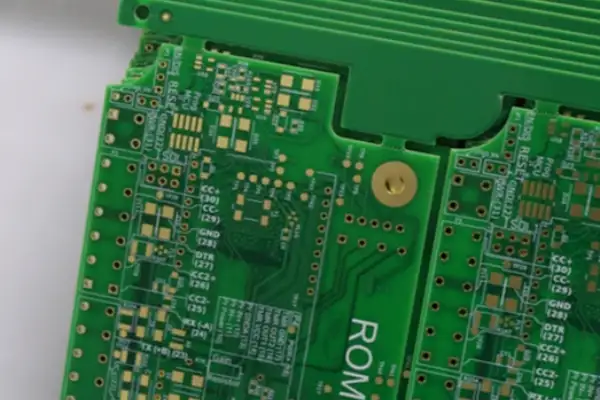
When I first started getting into millimeter wave circuit board design, I always thought it was very mysterious. When everyone mentions high-frequency signal transmission, they immediately bring up various complicated formulas and high-end-sounding materials, such as Rogers sheets. But to be honest, my experience tells me that what really determines the quality of a board is often not the expensive materials used, but whether the most basic processing techniques are in place. Take etching as an example. Many people think this is a mature process, but in the millimeter-wave frequency band, the challenges it brings are completely different dimensions.
Think about it, once the signal frequency reaches millimeter waves, the micron-level error is enough to make a huge difference in the performance of the entire circuit. Slight changes in line width, such as if you think it is just a few microns difference, will actually cause the characteristic impedance to completely deviate from the design value. I have seen some antennas and transmission line models that were beautifully drawn on the design drafts, and the simulation results were perfect. However, as soon as the test signal was put on the board, the signal was completely attenuated. This is often where the problem lies.
So now I pay special attention to the actual process capabilities of the processing plant rather than the top materials used in their brochures. A manufacturer that can stably control the precision etching process is much more reliable than a manufacturer that only sells high-end plates. For example, they need to be able to accurately manage the concentration, temperature and spray pressure of the etching solution, because these factors directly affect the uniformity of line width and verticality of sidewalls. A trace with sloping sidewalls will have unpredictable line width and impedance characteristics that deviate from the design.
Of course, material selection is not unimportant. Plates like Rogers that are optimized for high frequencies can indeed provide a more stable dielectric constant and help ensure signal integrity, but this does not mean that everything will be fine with it. The batch stability, hygroscopicity and resin flow control during lamination of the board also affect the dielectric constant distribution of the final product.
If the lamination process is poor, resulting in uneven thickness of the dielectric layer, the performance of the actual circuit board will be greatly compromised, no matter how good the parameters of the board itself are.
In one of my recent projects, we tried a mixed-material solution. Instead of using all expensive special boards, we made targeted material selection on key signal layers and strict processing control. In the end, the cost was well controlled and the performance was fully up to standard. Specifically, we use high-performance materials on the surface layer that carries the millimeter-wave antenna and front-end transmission lines, while using more cost-effective FR-4 materials in the inner digital control and power supply parts. This solution requires the factory to have superb craftsmanship when laminating different materials to ensure alignment and bonding between layers and avoid delamination under thermal stress.
This reminds me of another key point: the application of laser technology is becoming more and more common in high-frequency PCB manufacturing, especially when making tiny blind holes and fine lines. The precision of ultraviolet laser drilling is difficult to match with traditional mechanical methods. It can achieve very clean hole walls, which is crucial for high-frequency signal transmission because any burrs or irregularities will cause unnecessary signal reflection and loss. In addition, laser direct imaging technology is used for pattern transfer and can achieve higher alignment accuracy and finer line width than traditional film exposure. This is almost a necessary process for complex gradient lines or coupling structures on millimeter wave circuits.
After all, designing and manufacturing high-frequency circuit boards is a highly collaborative process. You can’t just throw the drawings to the factory and expect them to make perfect products. You must have a deep understanding of their process limits, such as what precision their etching lines can stably achieve and how small holes their laser equipment can make, and then adjust your design parameters based on these actual processing capabilities. For example, if the factory’s etching process best controls the uniformity of 10 mil line widths, then the design should try to avoid using 8 mil or finer line widths that are close to the limit of its capabilities, or evaluate the impact of process fluctuations in advance through simulation.
The armchair theoretical school and the hands-down craftsman school must sit together to actually make things and do them well. Designers need to explain the electrical significance of each critical dimension to process engineers, and process engineers need to provide feedback on the accuracy range that can be achieved repeatedly in actual production. This kind of early and in-depth communication is often much more efficient than repeatedly modifying and verifying problems after problems are discovered during testing, and can also avoid many costly reworks caused by “taking things for granted”.
I’ve seen too many people overcomplicate millimeter wave and high frequency circuit design. Everyone gets nervous when they mention mmWave PCB or high Frequency PCB. In fact, many times the problem is not that mysterious.
Many people are confused about what material to use Rogers or other boards. Of course, Rogers PCB is indeed good in some scenarios. The material properties are stable, but this does not mean that it is the only solution, and not all projects have to use such expensive materials.
My own experience is that what really determines success or failure is often not the material itself but how well you understand it and whether your processing plant can do it well.
For example, once we designed an antenna array using a plate that was not particularly high-end, but we spent a lot of time communicating with the factory to confirm the stacked impedance line width and even the etching factor of each layer several times before processing.
The result? The performance of the boards produced is much better than those designs that use the most expensive boards but are processed haphazardly.
This brings up a key point. Many people rely too much on so-called industry standards, such as the IPC series of standards. Of course they are very important. They are the common language and quality baseline of the industry.
But if you just mechanically copy these provisions and treat them as insurmountable iron laws, it may actually tie your hands and feet.
High-frequency circuit design sometimes requires a little flexibility and a deep understanding of the principles rather than whether a certain number absolutely meets the specifications.
I remember one time we encountered an impedance matching problem and couldn’t adjust it according to the conventional IPC guidance. Later, we put aside those rules and regulations and started from the basic principles of electromagnetic fields and changed a wiring structure and compensation method, and the problem was solved.
So my opinion is that standards and norms are your important tools and basis for communication, but they are not the end of your thinking.
What is really important is to establish your own set of design intuitions and a clear understanding of process boundaries. You have to know where you must strictly adhere to and where you can handle it flexibly.
After all, making high-frequency boards is a systematic project. From material selection to circuit design to processing and manufacturing, and finally to testing and verification, every link is closely connected. You cannot just focus on one part and ignore the whole.
Instead of blindly pursuing the top indicators, it is better to calm down and do each basic step to have a solid understanding of the true capabilities of the materials and processes in your hands. This will make it easier to make stable and reliable products. It feels much more fulfilling than simply stacking advanced parameters.
I recently talked with a few friends who are doing hardware about high-frequency circuit design. They always complain about why it is so difficult to build a mmWave PCB now. In fact, I think many people think about the problem in a complicated way.
Think about it, how could we pay so much attention to making ordinary RF boards in the early years? Just find any FR4 material and you can deal with the signal loss in the past. The higher the signal loss, the higher the frequency. Anyway, the impact is limited due to the low frequency. But things are different now. If the millimeter wave frequency is placed there, if the signal deviates slightly, the entire system may be useless.
I have seen many teams pursue the top Rogers materials right from the start, thinking that the more expensive ones are better. This idea is quite dangerous because materials are only the foundation. What really determines success or failure is design ideas and process control.
Take automotive radar as an example. Nowadays, people are talking about AEC certification. It seems that everything will be fine after passing this hurdle.
In fact, certification is just a ticket. The real test is the stability after mass production.
When an engineer I know and his team were making a 77GHz radar board, the performance in the laboratory was so good that the yield dropped to less than 70% when it came to mass production.
Later, it was discovered that the problem was due to the slight difference in the shrinkage rate of different batches of high-frequency plates in the lamination process, but it was this difference that caused the impedance to drift across the board.
It took them more than half a year to thoroughly understand the process parameters and now the performance of each batch of products is almost the same.
This reminds me of another interesting phenomenon. Many people think that military standards must be stricter than car regulations, but this is not necessarily the case.
Military products have high requirements for resistance to extreme environments, but the batches are usually small and quality can be ensured through screening.
Automotive electronics have to be installed in hundreds of thousands or even millions of vehicles, and stability must be built into the design and manufacturing process from the beginning. The idea of ”make it first and then screen it” simply does not work in the automotive field.
When it comes to domestic substitution, I think the biggest advantage of domestic manufacturers now is not cost but response speed.
The materials from large foreign manufacturers are indeed stable, but they may have to go through a half-year process to change the formula or adjust the delivery date. For domestic suppliers, if you submit your request in the morning, engineers can come to the site to debug together in the afternoon. This degree of cooperation is particularly valuable in a rapidly iterative project.
Of course, I’m not saying that domestic materials have completely surpassed foreign countries. In some ultra-low-loss application scenarios, imported materials still have irreplaceable advantages. But at least now we have the right to choose and no longer have to be stuck in a single supply chain. This is a good thing for the development of the entire industry.
Another point that is easily overlooked is the authenticity of the testing process.
Many companies will measure beautiful insertion loss and return loss under ideal conditions in order to make the data look good, but when the equipment is actually installed and surrounded by other circuit boards and metal casings, the performance is immediately compromised. Real engineering capabilities are reflected in the performance of the system after integration rather than the laboratory data of a single board.
I suggest that when doing high-frequency PCB, especially millimeter-wave related designs, don’t just focus on the board parameters and spend more time studying the entire signal path. From the antenna end to the processing chip, every link may become a bottleneck. Sometimes solving a grounding problem is more effective than replacing more expensive materials. This is probably the subtlety of engineering practice.
When doing millimeter wave PCB design, sometimes I really feel like I’m competing with the laws of physics. I’ve seen too many projects get stuck on signal integrity. Those traces that look perfect on the drawings are completely unrecognizable when tested in practice. Especially after reaching the millimeter wave frequency band, a slight impedance mismatch will cause the signal to attenuate terribly. At this time, choosing the right board material becomes particularly critical. Ordinary FR4 materials have too much loss at high frequencies and cannot be used at all.
Many people asked me what kind of board should be used as soon as I started, and whether I had to use Rogers materials. Actually, my view is a little different. Rogers PCB does perform stably in many high-frequency applications, and its dielectric constant and loss factor are well controlled, but it is not the only choice nor a panacea. You have to look at what product it is used on. For example, when some consumer electronics products are extremely cost-sensitive but require certain frequency performance, we may consider using composite sheets processed by other processes, or only use high-performance materials in the most critical RF front-end part.
This requires clear planning of partitions and stacking in the early stages of design, otherwise it will be very painful to revise later. A common strategy is to use a “hybrid stack” design that combines high-frequency sheets with low-cost materials in multi-layer boards, which requires designers to accurately calculate the electromagnetic field behavior at the interface of different materials and use simulation tools to pre-evaluate reflections and losses when signals are transmitted across areas.
When it comes to mass production, this is another level of challenge. Meeting the performance standards during the proofing stage is just passing the first level. The real test of skill is how to stably reproduce those precise line width and line spacing controls and complex hybrid lamination processes on thousands of boards. Millimeter wave PCB has almost strict requirements for the production environment – temperature, humidity, and cleanliness must be strictly controlled, otherwise impedance consistency cannot be guaranteed at all. Some factories I have worked with will tell you that they can make high-frequency boards, but you have to see whether their production lines have dedicated dust-free workshops, whether the testing equipment is advanced enough, and whether the operators have received systematic training. For example, it is crucial to control the uniformity of the thickness of the dielectric layer. Micron-level deviations may cause the characteristic impedance to exceed the tolerance range, thereby affecting the beamforming performance of the antenna array or the detection accuracy of the radar.
I always feel that being able to turn a complex millimeter-wave PCB from a drawing into a stable product and maintain a high yield reflects the comprehensive strength of a factory rather than just technical parameters. It involves the maturity of the process route, the rigor of the quality control system, and even the ability to grasp the quality of raw materials upstream of the supply chain. For example, the batch stability of high-frequency plates is very critical. If the dielectric constant of each batch provided by the supplier has slight fluctuations and your factory’s compensation process cannot keep up, the mass production yield will definitely go up and down. Excellent factories will establish strict incoming material inspection standards and have real-time monitoring and feedback systems that can instantly adjust etching parameters or lamination pressure on the production line to compensate for material fluctuations.
So when we evaluate a potential supplier, in addition to reading the successful cases and technical white papers they display, I would rather go to their workshop to see the actual production process and equipment status and chat with their front-line engineers. These details often explain the problem better than a gorgeous brochure. After all, in the field of high-frequency PCB, talking on paper will not work. Everything must rely on actual performance and data to speak for itself. For example, observe how they treat the surface roughness of copper foil. Because the skin effect is significant at high frequencies, the rough copper surface will introduce additional conduction losses, which requires specific processing processes to ensure.
Nowadays, more and more application scenarios are beginning to use millimeter wave technology, from 5G base stations to automotive radars to future satellite Internet terminals. This is both a huge opportunity and a real challenge for the entire PCB industry. This means that we can no longer be satisfied with the extensive production model of the past. We must improve precision, materials and process control to a higher level to seize the market opportunities brought by these high-end applications.
For example, automotive radar PCBs are required to work stably for a long time in extreme temperature changes and vibration environments, which puts the thermal expansion coefficient, lamination bonding strength and solder joint reliability of their materials to stringent tests that exceed those of conventional communication products.
Many people think that making high-frequency circuit boards is as simple as choosing expensive materials. I used to think so too. Later, after tinkering with a few boards myself, I discovered that this was not the case at all. Let’s take the most common FR4 and replace it with Rogers plate. Do you think it’s just a matter of replacing the substrate? The entire design idea has to change accordingly. The width of the traces needs to be recalculated. Even the size of the isolation ring around the via hole has to be adjusted. Otherwise, signal reflection will make you doubt your life.
I have seen many engineers think that high-frequency PCB design is too complicated. I always think that I need to use the most cutting-edge simulation software or the most expensive test equipment to complete the design work in the millimeter wave band. In fact, many times the problem lies in some basic places? For example, is the Rogers plate model you are using really suitable for your application scenario? The difference in dielectric constant temperature coefficient between different models is not small! If you work in an environment with large temperature changes, this detail can determine success or failure.
Speaking of the dimensionality of PCB design, I find it quite interesting! Nowadays, when everyone mentions high-frequency design, they only focus on the dimension of electrical performance! In fact, mechanical structure considerations are equally important! Will a board deform in a vibrating environment? Will the connector become loose due to mismatch in thermal expansion coefficient when installed? These mechanical dimension factors will ultimately affect the integrity of the signal! I have seen a case where failure to consider the position of the fixing screws caused resonance to occur at a specific frequency, raising the noise floor of the entire system by more than ten decibels.
I would like to say a few more words about the topic of domestic substitution! There are indeed many domestic high-frequency plate brands on the market now, and the prices are much cheaper than imported ones! But if you really plan to use it in a product, I suggest you do a full reliability verification first! It’s not that domestic products are not supported, but the consistency requirements for materials in high-frequency applications are too high! The dielectric constant of the same batch of plates fluctuates by a few percent, which may not be noticeable at low frequencies, but in the millimeter-wave frequency band, it is a huge difference!
Finally, let’s talk about craftsmanship! Many people think that if they hand over the design documents to the board manufacturer, everything will be fine! In fact, there are many details in the processing of high-frequency boards that require repeated communication and confirmation between you and the manufacturer! For example, the surface roughness treatment method of copper foil will directly affect the transmission loss performance of millimeter wave signals! There are also parameters such as temperature and pressure control during lamination that will change the dielectric properties of the final product!
After all, making high-frequency circuit boards is a process of constant trial and error and continuous learning. There is no one-and-done secret! You have to be willing to spend time understanding the material properties, figuring out the process details, and analyzing the test data! It’s not enough to just rely on the theories in books or other people’s experience summaries. You have to practice and experience it yourself to truly master it!
I think the future development direction of high-frequency PCB may focus more on system-level integration rather than simply pursuing the ultimate improvement of a single indicator! After all, in actual applications, every link in the signal chain will affect the final performance! Every connection and every transition from the antenna to the transceiver chip needs to be carefully designed and optimized!
Sometimes it’s interesting to think about how such a small circuit board actually contains so many physical principles and engineering wisdom! The sense of accomplishment every time you successfully make a high-frequency board with up-to-standard performance is truly indescribable in words! Although the process is excruciating, when the results come out, you will feel that all the effort was worth it!
I have always felt that many people’s understanding of high-frequency PCB design is a bit off. Everyone always discusses which Rogers board to use as soon as they start, or they are obsessed with how high the millimeter wave frequency band is. Of course these are important, but I think the core of the problem is often ignored: Was your design idea wrong from the beginning? I’ve seen too many engineers spend all their energy on material selection.
They think that as long as they use the best Rogers PCB materials or the latest mmWave PCB technology, the problem can be solved. The result? The performance of the board is still not good.
In fact, many times the problem lies in the most basic places – for example, you have not thought clearly about how the signal is going to go. High frequency signals are particularly sensitive and fragile.
It is not as tolerant of arbitrary layout and wiring as low-frequency circuits.
An unreasonable via location or a redundant trace may ruin the performance of the entire antenna.
My own experience is to first clearly draw the architecture of the entire system.
Don’t rush to open the design software.
First take a piece of paper or a whiteboard and walk through the signal link from beginning to end: Where does the signal come in, through which parts, and finally out? Where is the antenna placed? How to place the RF front-end?
Thinking these things through before taking action will save you countless troubles later. For example, knowing the direction of critical paths can help avoid running sensitive signal lines in parallel for long distances, thereby reducing crosstalk. Planning the separation of power and ground in advance can also prevent noise from coupling into the pure RF part from the source.
Another point is about the choice of materials.
Nowadays, there seems to be a trend that non-high-end materials do not think that only the most expensive Rogers boards can be used for high-frequency design.
This is actually a misunderstanding.
It is true that in some extreme application scenarios you need those low-loss high-frequency special materials, but in many cases ordinary FR4 materials with reasonable design can also meet the requirements.
The key is to know the characteristics of the material and then make trade-offs based on your specific needs.
Blind pursuit of high-end materials will only increase costs needlessly. For example, for certain digital control parts in 24GHz or 77GHz automotive radar modules, it is completely feasible to use FR4 with proven characteristics. This requires a clear understanding of the Dk (dielectric constant) and Df (loss tangent) of the material at different frequencies.
Speaking of cost, this is another issue that is easily overlooked.
Many people think that mmWave PCB design has to cost a lot of money because the technical threshold is high.
But in fact, costs can be effectively controlled through clever design.
For example, in a multi-layer board design, you can place millimeter-wave traces that require extremely high loss on the surface and low-frequency circuits that are less sensitive to loss on the inner layer. This can ensure performance without letting the cost get out of control.
Another example is that there are many mature solutions for antenna design that you can refer to. It is not necessary to design a brand new antenna structure from scratch.
Sometimes it is better to learn from existing successful cases and make adjustments according to your specific needs, which can also save a lot of simulation and testing time. For common patch antenna arrays or waveguide structures, there are a large number of public documents and design guidelines for reference, and you can just perform size scaling or impedance matching optimization.
I think the most taboo thing about high-frequency PCB design is working behind closed doors.
Nowadays, this field is developing so fast. New materials, new processes and new design concepts are emerging one after another.
If you don’t regularly follow industry trends and communicate with other designers, it’s easy to fall behind.
I spend some time every week reading the latest technical papers or going to professional forums to see what problems others have encountered and how they solved them.
This kind of continuous input is particularly helpful to me and often saves me a lot of detours. For example, learning about a new hybrid laminate structure or more efficient backdrilling technology may directly solve the return loss challenges you are experiencing on your current project.
The last thing I want to say is don’t think of high-frequency PCB design as too mysterious.
It does have its peculiarities but at the end of the day it is still part of electronic design.
As long as you master the basic principles and continue to accumulate experience in actual projects, you will slowly find the feeling.
It may feel difficult at first, but as long as you persist, you will find that it is not.
I used to think that doing high-frequency PCB design was just about choosing an expensive board and then drawing lines. It wasn’t until one of our projects that we used ordinary materials for millimeter wave circuit board prototype testing that we discovered that the problem was serious. Not only the signal is severely attenuated, but also inexplicable crosstalk often occurs.
Later, after talking to several experienced engineers, I realized that the doorway here is much more complicated than imagined. Factors that were originally negligible in the millimeter wave band have now become critical issues. Details such as the surface roughness of the plate will directly affect the signal transmission quality. The dielectric constant of the conventional materials we used before will become very unstable in a high-frequency environment, causing the impedance matching to be incorrect no matter how adjusted it is.
After that failure, I began to study various specialized high-frequency materials and found that the product characteristics of different manufacturers are actually quite different. Some materials are stable within a certain frequency range but exhibit various problems at higher frequencies. This made me realize that choosing a suitable high-frequency PCB material should not just look at the numbers on the parameter table, but also need to be judged based on the actual application scenario.
Impedance matching becomes particularly delicate in high-frequency designs.
The simple calculation method we are used to before is simply not enough in the millimeter wave frequency band because even the curvature of the trace corners will affect the final effect. I remember a project that repeatedly adjusted the layout more than a dozen times in order to optimize an antenna matching network. Each small change would bring measurable performance changes.
The importance of the etching process is also often underestimated. Many manufacturers advertise that they can produce fine lines, but the actual edge roughness simply does not meet the requirements for high-frequency applications. I’ve seen some samples where the trace edges look like jagged edges when viewed under a microscope. This rough surface creates additional losses at high frequencies.
Now when I encounter millimeter wave-related designs, I will pay special attention to the actual high-frequency characteristics of the material instead of just looking at its nominal highest frequency. Sometimes in order to obtain better performance, it is better to spend more money and choose those proven high-frequency special materials, because the losses caused by later debugging failures are often greater.
I think the most important thing that needs to be changed in high-frequency design is that the way of thinking can no longer be applied based on the experience of low-frequency circuits. Every detail may become a bottleneck. From plate selection to processing technology to final testing, the cognitive system needs to be re-established. This is indeed a process of continuous learning and adjustment.
High-frequency PCB design is not metaphysics; senior engineers share real experience. In
The motor drive circuit board in industrial equipment failed after long-term operation,
Many 5G antenna PCB designs rely too much on simulation, but ignore
- Эксперт в области мелко- и среднесерийного производства
- Высокоточное изготовление печатных плат и автоматизированная сборка
- Надежный партнер для электронных проектов OEM/ODM
Часы работы: (пн-сб) с 9:00 до 18:30