
How to Choose an Excellent Semiconductor Flex PCB Manufacturer?
While collaborating with a smart wearables team to select a semiconductor flex
Having worked in the high-frequency microwave board industry for a long time, I’ve gradually noticed an interesting phenomenon. Many people’s first reaction upon receiving a board is to immediately measure parameters, wanting to connect the instruments and see the results instantly. But what truly determines performance is often not how accurate the measurement itself is, but whether the preliminary preparation is adequate. I’ve seen too many cases where neglecting this crucial step led to completely distorted data.
I remember once taking on a project where the client requested a full S-parameter analysis of a batch of high-frequency microwave boards. The team immediately set up the equipment, only to find the measured curves fluctuating wildly. After three reworks, we finally realized the problem lay in the seemingly tiny oxide layers on the connectors, which directly altered the impedance characteristics at high frequencies.
This experience taught me a valuable lesson: in the high-frequency field, calibration is not a routine task but the cornerstone of the entire process. Even with the most advanced vector network analyzer, if calibration components are worn or connectors are loose, all the data becomes a numbers game.
Later, we adjusted our workflow. Now, the first thing we do when each batch of boards arrives in the lab isn’t immediately powering them on, but spending half an hour checking all the interfaces, wiping the probes with alcohol swabs, and verifying the connection tightness with a torque wrench. This seemingly clumsy approach has actually increased testing efficiency by 30% because the number of repeated measurements has been significantly reduced.
One detail that might be easily overlooked is that ambient temperature has a more sensitive impact on parameters than one might imagine. Especially in summer, even a 0.5-degree fluctuation in the lab’s air conditioning can cause insertion loss values to drift by 2% in certain frequency bands. Now, we include the measured temperature and humidity in our reports, even if customers don’t necessarily look closely, it shows respect for the accuracy of the data.
Recently, we encountered a new situation: the nominal and measured dielectric constant values of a batch of boards showed slight deviations. The supplier insisted their quality control was fine, but through repeated verification using the resonant cavity method, we found that there was indeed a thousand-level fluctuation between batches. Such subtle differences might be insignificant in low-frequency circuits, but for millimeter-wave design, it’s a critical point.
Therefore, I increasingly feel that quality control of high-frequency boards is more like detective work. Focusing solely on the final parameters can easily lead to misconceptions; sometimes, it’s the seemingly insignificant aspects, such as the cleanliness of the fixtures or the strict adherence to calibration cycles, that are the key to breaking the deadlock. After all, when signals reach 77GHz and above, no detail is trivial.
Having worked on high-frequency microwave boards for years, I’ve come to understand that choosing the right supplier is more important than anything else. Sometimes, looking at the materials of manufacturers who boast about their capabilities gives me a headache—very few can truly handle high-frequency microwave boards. I’ve seen far too many people fail at the testing stage. A colleague of mine, working on a 77GHz project last year, hired a supplier with an extremely low price. Every time they tested data, they had to send it to an external lab. After a month of back-and-forth, they discovered the board’s performance was unstable and unusable. Later, they switched to a manufacturer with in-house testing capabilities, and the problem was solved.
Currently, there are very few PCB suppliers in the industry with truly comprehensive testing capabilities. Especially when it comes to high-frequency parameter verification, you simply can’t do it without specialized equipment. One manufacturer I’ve worked with has its own anechoic chamber and probe station, capable of testing everything from material properties to finished product performance. This self-inspection capability really saves a lot of trouble.
Actually, there’s a simple way to judge whether a supplier is reliable: see if they dare to make their test data transparent. Good manufacturers will proactively provide complete parameter reports, clearly indicating even batch differences in materials, while some will only vaguely say “meets industry standards.” With microwave boards, even the slightest error can have huge consequences; without detailed data support, it’s just gambling.
Recently, while working on a 94GHz project, I found that even traditional large manufacturers stumbled at the testing stage. Although the outsourced labs they used had advanced equipment, the testing conditions for different batches of boards were inconsistent, leading to data discrepancies. This detail exposes a loophole in supply chain management.
I believe the future development of high-frequency boards will increasingly rely on the comprehensive capabilities of manufacturers. Good materials alone are not enough; matching process control and testing methods are essential. The trend is towards a fully controllable model where some emerging manufacturers move testing upstream in the production process, setting up testing points at every key stage.
Having worked on high-frequency microwave boards for years, I’ve come to understand that the real headaches aren’t the complex theoretical calculations, but rather the seemingly basic material properties and processing details. For example, when using PTFE as the substrate, many initially think it’s a good choice due to its stable performance and low loss. However, the real problems only begin on the production line.
I remember once we were making a millimeter-wave band board with extremely high precision requirements; the linewidth tolerance had to be controlled within a very small range. At that time, conventional exposure equipment simply couldn’t meet the requirements. We eventually switched to LDI direct imaging to barely pass the test. But that wasn’t the end of the story. Later, the side etching problem arose; even slight miscontrol of the linewidth resulted in deviations from acceptable limits. This millimeter-level precision challenge permeated almost the entire manufacturing process. For example, when fabricating antenna arrays above 30GHz, a linewidth deviation exceeding 5 micrometers would cause phase errors, directly affecting beamforming. We had to introduce an online optical measurement system to monitor the etching rate in real time and dynamically adjust the chemical parameters to maintain stability.
Another time, when metallizing PTFE material holes, we tried several methods. Ordinary chemical copper plating simply couldn’t adhere to the palladium catalyst hole walls; copper simply wouldn’t adhere. Later, we tried plasma treatment, bombarding the hole walls in a vacuum environment, which was indeed more effective than traditional methods, but equipment cost and process stability became new problems. Especially when processing deep blind holes with a thickness-to-diameter ratio greater than 8:1, the plasma struggled to uniformly cover the hole bottom, often resulting in good metallization in the upper half but insufficient adhesion in the lower half. This forced us to add a sodium naphthalene solution activation step before plasma treatment, using chemical etching to increase the specific surface area of the hole walls and improve adhesion.
What impressed me even more was the dimensional stability problem during multilayer board lamination. PTFE material has a relatively large coefficient of thermal expansion, which varies in different directions. If the temperature and pressure curves are not properly controlled during lamination, the board dimensions will drift. We once encountered a situation where the inner layer alignment was completely off after lamination, which could only be compensated for by X-ray drilling, but this increased the complexity of the process. In fact, we later discovered that different batches of PTFE substrates exhibited a ±15% fluctuation in the Z-axis coefficient of thermal expansion, requiring each batch of material to undergo re-verification of the lamination process. To address this, we established a material database, recording the Dk/Df values and thermal expansion characteristics of each roll of material, and conducted small-scale trial laminations before lamination to optimize parameters.
Surface treatment was also a challenge. The nickel layer in conventional immersion gold processes caused significant magnetic loss in the millimeter-wave band. We later solved this problem by using nickel-free direct immersion gold. However, for antenna applications, sometimes bare copper or immersion silver is more suitable, but this requires considering the balance of oxidation resistance. Especially in automotive radar applications, our tests revealed that after 2000 hours of operation at 85℃/85%RH, the surface resistivity of immersion silver treatment increased by approximately 8%. However, choosing an organic solder resist agent combined with selective gold plating ensured both high-frequency performance and met automotive-grade weather resistance requirements.
Speaking of back-drilling, it truly tests the limits of machining precision. At high frequencies, even a difference of a few tenths of a millimeter in the length of the residual spike in the through-hole can introduce significant signal loss. Our tests showed that even a small change in the length of the residual spike in the 77GHz band can indeed have a measurable impact. The most challenging issue is that when the board thickness exceeds 2.4mm, the spindle runout of a conventional mechanical drilling machine can cause fluctuations in the back-drilling depth of ±50 micrometers. Later, we introduced laser back-drilling technology, using CCD visual positioning and real-time depth monitoring to improve the residual spike control precision to within ±10 micrometers, but this increased the processing cost by 30%.
These experiences made me realize that manufacturing high-frequency microwave boards is like walking a tightrope; every step requires extreme caution. Sometimes, the theoretically optimal solution may encounter unexpected obstacles in actual production. What truly matters is a deep understanding of material properties and precise control over process details—this is far more practical than any theoretical calculation.
Looking back, the pitfalls I encountered over the years have become invaluable lessons. After all, theoretical discussions alone are far from sufficient in this field; only hands-on experience can reveal the delicate balance points.
Recently, while researching applications of high-frequency microwave boards, I discovered an interesting phenomenon—many people focus on the visible antennas and chips. However, the fundamental materials that truly determine the performance of millimeter-wave systems are often overlooked. Just as you can’t build a house by focusing solely on the interior design while ignoring the foundation quality.
I remember encountering signal attenuation issues last year while working on an automotive radar project. The team spent a significant amount of time adjusting the antenna design with little success until we turned our attention to the substrate material carrying the circuitry. That experience made me realize that for millimeter-wave technology to achieve true breakthroughs, we must pay attention to these seemingly ordinary components; they are the invisible skeleton supporting the entire system.
Currently, many manufacturers are pursuing higher frequencies but neglecting the limitations of the materials themselves. High-frequency microwave boards not only need to meet signal transmission requirements but also need to consider parameters such as thermal expansion coefficient and dielectric constant stability, which directly affect system reliability in extreme environments. I’ve seen too many projects experience frequent problems later on due to improper selection of basic materials.
Interestingly, additive manufacturing technology is bringing new ideas to this field. Although still in the exploratory stage, directly printing circuits on 3D curved surfaces can indeed overcome some limitations of traditional processes. However, commercialization requires overcoming challenges in material compatibility and mass production stability, which necessitates collaborative innovation across the entire industry chain.
When choosing suppliers, I value their technological expertise more than price advantages. After all, millimeter-wave applications have extremely high precision requirements; even micron-level deviations can lead to significant performance degradation. Finding a partner who truly understands material properties upfront is far more important than any short-term cost savings than post-construction fixes.
I recently chatted with a friend who works in automotive radar and discovered an interesting phenomenon. Their team spent over half a year debugging a 77GHz radar module whose performance was consistently unstable. They later discovered that this was caused by the dielectric constant drift of the PCB board under high-frequency conditions. This reminds me that many engineers today focus on chip selection while neglecting the fact that the high-frequency microwave board supporting these chips is the true cornerstone of performance.
Millimeter-wave technology brings not only speed improvements but also a revolution in traditional circuit design concepts. Last year, in a satellite communication project I participated in, we tested microwave boards from different suppliers. One manufacturer’s sample showed excellent performance in a laboratory environment, but signal attenuation worsened immediately in outdoor environments with drastic temperature differences. It was later discovered that the mismatch between the thermal expansion coefficient of the substrate and the copper foil caused microstrip line deformation invisible to the naked eye. Although this deformation is only at the micrometer level, in the 79GHz band, it is enough to cause a significant phase shift in electromagnetic waves, leading to beam pointing deviations in the array antenna. Satellite communication antennas typically use phased array designs, and the phase error of each radiating element directly affects the signal coverage.
The real test for high-frequency microwave boards is how to maintain stable electromagnetic characteristics in extreme environments. For example, autonomous driving radar must withstand the high temperatures of the engine compartment and cope with the corrosive effects of rain and humidity. Ordinary FR4 material in the millimeter-wave band is like a leaky pipe, with most of the signal lost before it even reaches its destination. Professional microwave boards, on the other hand, can concentrate and transmit energy like a precision conduit. Especially in humid environments, the water absorption rate of ordinary boards causes changes in the dielectric constant, while microwave boards typically reduce hygroscopicity by adding ceramic fillers or using a PTFE substrate. Experimental data shows that after 24 hours in an 85% humidity environment, the loss tangent of FR4 increases by about 30%, while the change in high-performance microwave boards can be controlled within 5%.
A common misconception is that using high-end materials solves all problems. In reality, we’ve encountered circuit boards using top-tier Rogers materials where improper lamination processes resulted in micro-bubbles between layers. These bubbles become sources of electromagnetic wave scattering in the 79GHz band. The problem was only resolved after adjusting the lamination temperature profile. This made me realize that materials and processes are like a bow and arrow—both are indispensable. In the lamination process of multilayer boards, precise control of the heating rate and pressure profile is necessary to allow the prepreg to flow fully without over-extruding it. Our ultrasonic scanning revealed that when the bonding temperature deviation exceeded 5°C, clusters of bubbles with diameters of 50-200 micrometers appeared between the layers. These bubbles are equivalent to countless miniature mirrors in the millimeter-wave frequency band.
Many manufacturers like to advertise ultra-low loss specifications, but in practical applications, stability is often more important than theoretical values. Just like the most reliable equipment for mountaineering isn’t the lightest piece, but the one that maintains its performance in a blizzard. For high-frequency design, a microwave board that can operate continuously for ten years at temperatures ranging from -40°C to 85°C is far more valuable than a laboratory sample with impressive specifications but no mass production capability. Especially in automotive electronics, components need to withstand temperature cycling for more than 10 years, meaning the glass transition temperature of the microwave board must be at least 30°C higher than the maximum operating temperature; otherwise, the material will undergo plastic deformation. We compared two boards with similar loss values. After 1000 temperature cycles from -40°C to 125°C, one board showed an insertion loss change of 15%, while the other kept it within 3%.
Recently, I’ve seen some designs adopting hybrid dielectric layer structures. For example, using high-frequency specialized materials in critical signal layers and lower-cost materials in other layers—a concept similar to using high-quality materials for load-bearing walls in construction. However, this structure places extremely high demands on the bonding process; poor flow control at high voltages can lead to impedance abrupt changes. When designing hybrid dielectric boards, special attention must be paid to the matching of dielectric constants of different materials. For example, if the RF layer uses PTFE with a dielectric constant of 2.2, while the general layers use FR4 with a dielectric constant of 4.5, signal reflections will occur in the transition region. The solution is to create a gradient structure between layers, or to choose a combination of materials with a dielectric constant difference not exceeding 0.8.
Ultimately, high-frequency circuit design is akin to crafting a Swiss mechanical watch: every component must coordinate with precision at a microscopic scale. When electromagnetic wavelengths shrink to the millimeter range, even the thickness of the solder mask can impact performance—a level of precision that borders on the realm of semiconductor manufacturing. In the future, PCB fabrication plants may need to maintain the same temperature- and humidity-controlled environments found in wafer fabs to successfully produce qualified millimeter-wave substrates. Currently, leading manufacturers of microwave substrates have already begun utilizing cleanroom environments for critical processes, particularly during the pattern transfer and surface treatment stages. Since millimeter-wave transmission lines typically measure only 100 to 200 microns in width, the presence of even a single dust particle can cause deviations in line width, thereby altering the characteristic impedance. Studies indicate that in the 77 GHz band, a deviation in transmission line width exceeding 8 microns can result in a fluctuation of 0.5 dB in insertion loss.
I’ve been pondering the design of high-frequency microwave boards lately. Many people think it’s incredibly mysterious and complex. Actually, it’s not that esoteric.
I remember discovering an interesting phenomenon while working on a millimeter-wave project: sometimes we focus too much on theoretical calculations and neglect the impact of actual manufacturing processes. For example, the choice of copper foil is particularly crucial.
During our testing of different boards, we found a pattern—materials that appear similar on the surface can perform very differently in real-world applications. Especially at higher frequencies, you’ll find that the inherent characteristics of the dielectric material are less critical; rather, the influence of the conductor becomes more pronounced.
An interesting observation: we tried various high-end substrates to reduce losses, and found that the most significant improvement came from replacing the copper foil with a smoother one.
Millimeter-wave design definitely requires a change in thinking; traditional methods easily run into obstacles here.
I’ve seen many engineers habitually apply low-frequency design approaches, resulting in various strange problems during testing. These problems often stem from the most basic aspects, such as the surface treatment of the circuitry or grounding design. These seemingly insignificant details are magnified many times over in high-frequency environments.
When it comes to losses, many people’s first reaction is to choose more expensive substrate materials. However, the reality is that there may be more room for optimization in the conductor, especially when the frequency enters the millimeter-wave band, where the current is concentrated in that thin surface layer. At this point, the quality of the copper foil directly determines the overall performance.
We conducted comparative experiments; the same design using copper foil treated with different processes resulted in nearly double the insertion loss—and this was under completely identical conditions.
High-frequency microwave board design requires more consideration from an electromagnetic field perspective, not just a circuit-centric approach. Sometimes, fine-tuning the wiring or changing the location of grounding holes can have a more noticeable effect than changing materials. Of course, this requires accumulating practical experience to grasp those delicate balance points.
I think the biggest taboo in this field is blindly applying methods; each project has its own unique characteristics and requires specific analysis.
Having worked with high-frequency microwave boards for years, I’ve come to realize that choosing the right material is like choosing the right tires for a race car. You can use ordinary tires to drive at high speeds, but on the racetrack, those subtle differences can be the deciding factor.
I remember when we first worked on a 77GHz project, someone on the team insisted on using conventional low-loss boards, resulting in radar systems that always fell short. Later, we switched to a PTFE substrate, and the entire system’s response speed immediately changed—it was like paving a highway for the signal.
Many people think high-frequency design is just about adjusting parameters, but the stability of the material is key. Ordinary boards perform well at low frequencies, but at millimeter-wave frequencies, even a slight shift in dielectric constant causes impedance problems. It’s like walking on flat ground and suddenly stepping on sand; every step requires readjusting your balance.
In one test, we compared PTFE substrates from different suppliers and found that although the nominal parameters were similar, the phase consistency at 77GHz differed significantly. It was like writing with two pens of the same model but from different batches; the stability of the pen strokes was simply not on the same level.
Now, seeing people in the industry still using generic materials for high-frequency projects, I always want to remind them—in the millimeter-wave world, materials are not a cost factor but the cornerstone of performance. The little bit of cost you save on board material will eventually become the cost of overtime work during debugging.
I’ve recently been researching high-frequency microwave board material selection, which is quite interesting. I used to think that as long as the electrical performance was good, everything would be fine, until I actually worked on several projects and realized that it’s not that simple at all.
For example, once we tried using LCP to make an antenna board for a wearable device. Although its dielectric loss was indeed very low, delamination always occurred during multilayer lamination. Later, we switched to modified polyimide. Although the parameters were slightly inferior, the yield rate doubled. This lesson made me realize that there is often a huge gap between theoretical parameters and actual production.
The performance of ceramic substrates in base station power amplifier modules is indeed impressive, especially the thermal conductivity of aluminum nitride, which can reduce chip temperature by more than 20°C. However, its brittleness is a major issue; even slight bumps during transportation can cause microcracks—a hidden problem that is impossible to detect during testing.
I now prefer to view materials as dynamic systems rather than static parameter tables. Take the common modified PTFE as an example: although the original version has dimensional stability issues, reinforcement with glass fiber cloth retains its high-frequency advantages while solving processing difficulties. This balance is the essence of engineering practice.
A client once insisted on pursuing the lowest loss factor and chose a special ceramic material. Later, it was discovered that the raw material cost alone accounted for 40% of the entire project budget. This made me realize that discussing material performance without considering the application scenario is just theoretical.
In fact, choosing materials is like matching clothes; it’s not just about the quality of individual pieces but also about overall harmony. Sometimes sacrificing a little theoretical performance for better process adaptability can make the final product more competitive. This trade-off requires a lot of practical experience to grasp accurately.
Making high-frequency microwave boards truly tests one’s patience and expertise. Sometimes you receive a board that looks fine at first glance, but it just doesn’t perform right in practice. That’s when rigorous testing procedures are crucial.
I remember a project where we almost had a major problem because we overlooked some details. The high-frequency microwave boards we used appeared to meet standards, but in practice, the signal transmission was consistently unstable. After careful investigation, we discovered it was due to the inherent characteristics of the materials themselves. Although the parameters provided by the supplier were within the standard range, the actual performance just didn’t meet expectations.
Speaking of delivery time, I think many people fall into a misconception—that faster is always better. In reality, truly reliable high-frequency boards often require a longer production cycle because everything from raw material selection to processing technology needs to be extremely meticulous. Once, we chose a solution with a short delivery time to meet a deadline, but ended up wasting even more time due to rework.
Now, my selection criteria for high-frequency circuit boards have completely changed. I no longer simply look at the specifications; I focus more on the compatibility with the actual application scenario. For example, the requirements for high-frequency boards used in communication base stations and medical equipment are completely different. The former may prioritize stability, while the latter has higher precision requirements.
Testing is a crucial step that cannot be skipped. Some people think that as long as the design is sound, everything is fine. However, every step from materials to finished product can affect the final performance. Our current approach is phased testing, starting with raw material warehousing, to identify problems as early as possible.
Speaking of supply chain management, I believe the most important thing is to establish long-term, stable partnerships. Instead of constantly searching for the lowest-priced supplier, it’s better to invest time in cultivating a few truly knowledgeable partners. They can provide professional advice based on your specific needs, which is especially important in high-end fields.
The deepest lesson I’ve learned in this industry is that details determine success or failure. Sometimes, a seemingly insignificant adjustment to a process parameter can have a huge impact on overall performance. Therefore, we now maintain high standards at every stage, willing to spend more time to ensure quality.
A recent new project gave me a deeper understanding of high-frequency board materials. I initially thought that simply using the best materials was enough, but I later discovered that design and layout are equally critical. The same materials perform very differently under different design schemes, which made me realize that I must consider problems from a systemic perspective.
Ultimately, producing high-frequency microwave boards requires comprehensive professional capabilities. From material selection to process control, from testing and verification to supply chain management, every step requires meticulous attention. Only by doing all of these things well can the reliability and performance of the final product be guaranteed.
I now place particular emphasis on accumulating practical application data. After each project, I compile detailed usage reports; this firsthand data is invaluable for subsequent improvements. After all, no matter how impressive the theoretical parameters are, they are not as convincing as actual measured data.
Regarding supplier selection, I think the most important thing is their professional attitude. Some manufacturers, although small in scale, are extremely meticulous about technical details; such partners are often more trustworthy. Conversely, some large manufacturers, due to their rigid processes, sometimes lack flexibility.
Finally, I want to say that this industry truly requires patience and slow, deliberate refinement. Being impatient for quick results often backfires; only by perfecting every detail can truly high-quality products be made.
Every time I see those intricate high-frequency microwave board design drawings, I recall my first experience with RO3003 material. Back then, our team was working on a millimeter-wave radar project. We initially used ordinary FR4 board material, but the signal attenuation was severe—it felt like running through mud. Later, when we switched to RO3003, we discovered how significant the dielectric loss of the material itself had on high-frequency signals. For example, in the 24GHz band, the loss tangent of FR4 was as high as 0.02, while RO3003 could control it to within 0.0013. This tiny difference accumulated into a significant difference in signal integrity over long distances.
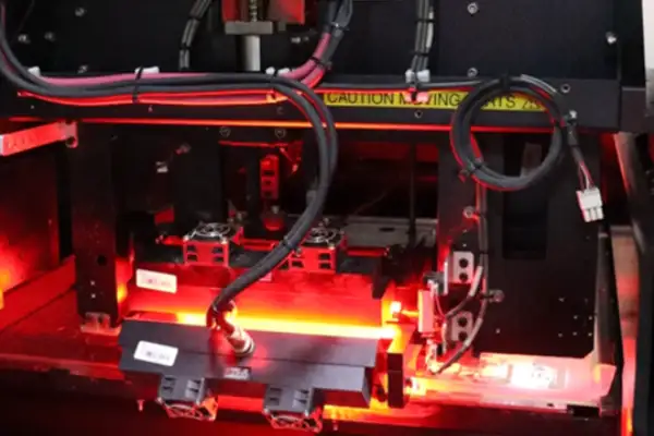
Drilling is truly a technical task. Once, a supplier delivered boards with hole walls as rough as sandpaper, causing poor plating adhesion. We later replaced them with special drill bits and used more precise spindle speed control to solve this problem. Now, seeing those smooth hole wall cross-sections reminds me of the days spent repeatedly adjusting parameters. Through experiments, we found that when the spindle speed is stabilized at 180,000 rpm and the feed rate is controlled at 1.2 m/min, the optimal hole wall quality can be obtained. This parameter combination is particularly suitable for machining micro-holes smaller than 0.3 mm.
In fact, the worst thing in high-frequency circuit design is compromise. I’ve seen cases where people compromised on materials to save costs, resulting in the entire board being redesigned. Especially for equipment like 5G base stations that require long-term stable operation, material selection directly impacts later maintenance costs. Sometimes, spending 30% more on materials can save 50% of the debugging time later. For example, a customer once insisted on using a low-cost substrate, resulting in frequency deviation due to fluctuations in dielectric constant caused by changes in ambient temperature. Ultimately, an additional heat dissipation module had to be added to compensate for the performance loss.
Recently, while testing a 40GHz board, I discovered an interesting phenomenon: the same wiring scheme using RO3003 boards from different manufacturers showed a 0.2dB difference in insertion loss. This made me realize that in addition to nominal parameters, actual batch stability must be considered. Now, every time new materials arrive, small-scale testing is conducted first. We have developed a rapid verification process that uses a TDR (Time Domain Reflectometer) to measure signal propagation speed and combines it with a vector network analyzer to scan the entire frequency band, completing the verification of key parameters within two hours.
Speaking of processing precision, I was deeply impressed by a visit to a military enterprise’s production line. They used microscopes to inspect the smoothness of each hole wall, not even overlooking micron-level burrs. This rigorous attitude is indeed worth learning, as the sensitivity of high-frequency signals to defects is beyond imagination. Especially in the millimeter-wave band, surface roughness can trigger the skin effect, leading to increased conductor loss. This is why they insist on performing three electroplating fill treatments on each via.
Flexible circuit boards are now also using LCP material, but the processing is more difficult. I remember once failing three times trying to drill vias in curved sections before finally mastering the appropriate drilling parameters. That’s how this industry is; every detail can be a stumbling block. We found that LCP material is prone to leaving molten residue during drilling, requiring a stepped drilling strategy: first, use a 0.1mm drill bit to create a pilot hole, then use a drill bit of the target size to enlarge the hole, while strictly controlling the drill bit dwell time to prevent overheating.
Recently, while collaborating with automotive radar manufacturers, we found their requirements for material consistency to be almost demanding, as it relates to the safety of autonomous driving. This prompted us to establish a more stringent incoming material inspection process. Now, every batch of RO3003 undergoes dielectric constant sampling testing. We introduced a statistical process control method, taking samples from three different locations on each roll of material, requiring the dielectric constant fluctuation range to be controlled within 2.97±0.04; anything exceeding this tolerance is immediately returned.
Sometimes, I feel that making high-frequency boards is like creating micro-sculpture art. It requires both a macroscopic design concept and the ability to control the physical properties of the microscopic world. The sense of accomplishment is especially real when you see those complex multilayer boards displaying perfect S-parameter curves on a network analyzer. For example, the 77GHz automotive radar board I recently completed achieved 0.1mm blind via interconnection in a 32-layer lamination structure, with a return loss of less than -25dB. This level of precision requires that the width tolerance of each impedance control line cannot exceed ±0.003mm.
While collaborating with a smart wearables team to select a semiconductor flex
We often regard electronic products as a glossy whole, but ignore the
Many assume that choosing China for PCB assembly is solely about saving
- Эксперт в области мелко- и среднесерийного производства
- Высокоточное изготовление печатных плат и автоматизированная сборка
- Надежный партнер для электронных проектов OEM/ODM
Часы работы: (пн-сб) с 9:00 до 18:30