
Industrial Automation PCB Reliability: How to Achieve 10+ Years of Stable Operation
In the field of industrial automation, people often pay attention to AI
I’ve always felt that the most fascinating aspect of miniature circuit boards isn’t the high-end equipment specifications, but rather the almost handcrafted precision involved in their fabrication. I remember visiting a friend’s lab once and seeing them working with lines finer than a hair; it suddenly dawned on me that this field is more like micro-sculpting art.
Those densely packed miniature circuit boards feel light in your hands, but every detail holds immense expertise. For example, in the etching process, experienced workers judge concentration by observing the solution’s color changes—more accurately than instrument readings. Once, they received an order for medical equipment; because the circuitry was so dense, the etching process almost ruined the entire batch—broken lines here, residue there. They later discovered that fluctuations in the workshop’s temperature and humidity affected the solution’s activity.
The hole wall treatment is even more of a test of patience. I’ve seen beginners create rough hole walls, resulting in severe signal attenuation after power-on. An experienced worker taught me a simple method: using a microscope to monitor the copper plating process, immediately adjusting the current parameters when bubbles appear. Although laser drilling is now used, that intuitive judgment of metal fluidity can never be replaced by machines.
What impressed me most was their board repair work. Using probes finer than sewing needles to repair circuitry, they had to hold their breath, knowing that a slight mistake could puncture adjacent lines. After doing this kind of work for a long time, even threading a needle became incredibly skillful.
Perhaps it is precisely this accumulation of seemingly insignificant experience that imbues cold electronic components with warmth. Now, every time I see a circuit board in a mobile phone, I think of those figures hunched over microscopes—no matter how advanced the technology, ultimately, it is human skill and craftsmanship that support the limits of precision.
Recently, while researching microelectronic devices, I discovered an interesting phenomenon: the most ingenious designs often rely on a special type of circuit board—a rigid-flex structure. This design is particularly common in wearable devices and medical implants because it perfectly balances stability and flexibility.
I remember once disassembling a smart bracelet and finding that its motherboard used this technology. The rigid parts firmly supported the main chip and sensor components; while the curved parts connecting the screen folded softly like ribbons within the confined space. This design made me realize that the evolution of electronic products is essentially a continuous challenge to the limits of physical space.
Many medical devices are now also adopting this miniaturization design approach. For example, some implantable monitoring devices need to operate within the human body for extended periods; their multi-layered precision circuitry must simultaneously meet biocompatibility and signal stability requirements; this made me realize that the choice of circuit board materials is more important than I had imagined.
Traditionally, we’ve always thought that the rigider electronic components, the better; however, in certain scenarios, a degree of flexibility can actually bring better adaptability. Just like a plant’s root system can both stabilize its growth and adjust its direction according to changes in soil shape, the concept of combining rigidity and flexibility aligns with this natural wisdom.
I’ve noticed that even drones are now adopting this design extensively, especially those models that require folding wings; their control modules are often embedded in the movable joints. This three-dimensional wiring approach completely breaks the limitations of planar circuits.
Sometimes I think: perhaps the form of future electronic products will increasingly resemble biological tissue; possessing both skeletal support structures and muscular elastic adaptability; and all of this will begin with breakthroughs in these seemingly insignificant micro-circuits.
I’ve always found those tiny, exquisite Miniature Circuit Boards particularly fascinating. They look simple, yet they conceal a great deal of complexity.
I remember once disassembling an old radio and finding a circuit board about the size of my palm, densely packed with components. This kind of micro-design actually demands careful attention to every step of the manufacturing process, otherwise, problems can easily arise.
What impressed me most during the testing process was the meticulous scrutiny required, examining every single scratch, even the finest hair. Once, I encountered a board that looked fine on the surface, but after powering it on, a certain area would consistently overheat; it turned out to be a tiny internal short circuit.
During testing, we had to simulate various operating environments—high temperature, low temperature, humidity, and dryness—all had to be tested. I’ve seen boards that functioned normally at room temperature but malfunctioned upon exposure to moisture, indicating inadequate moisture protection.
Quality control isn’t just about looking at the appearance. For example, a slight deviation in the position of a via could render the entire board unusable. Once, several boards in a supplier’s batch had to be returned because the via diameter error was 0.02 millimeters too large.
Electrical performance testing is even more critical. If the on-resistance is too high, signal transmission will be delayed. I habitually use a multimeter to repeatedly test critical points, sometimes ten times or more, before I’m satisfied.
These experiences taught me that in the manufacturing of micro-circuit boards, every step is crucial. From design to finished product, every detail must be meticulously considered; otherwise, even the best design is wasted.
Now, when I see sophisticated electronic devices, I always think of those unassuming little circuit boards behind them—the true skeleton that supports the entire system.
I’ve always found those tiny electronic devices particularly fascinating. The things you hold in your hand are so light and simple, yet they can perform so many complex tasks. Behind this lies those miniature circuit boards, almost invisible to the naked eye. They’re like the nervous system of the device, responsible for transmitting various signals and information.
I remember once disassembling an old hearing aid; it was densely packed with various circuits, yet the overall design was incredibly compact. That’s the charm of microtechnology—condensing complex circuits into a tiny space and maintaining stable operation. This truly requires a high level of craftsmanship. Many medical devices are now developing in this direction; after all, patients need lightweight comfort, not cumbersome burdens.
Speaking of these miniature circuit boards, what I find most astonishing is their interconnection method. Ensuring reliable connections with such tiny lines is no easy feat. I’ve seen some early products suffer from unstable performance due to interconnection problems. Modern technology has advanced significantly; through more precise manufacturing processes, these connections have become much stronger. Reliability reminds me of my old radio repair experiences. Back then, the circuitry was relatively simple; the miniaturization trend has changed everything.
In fact, it’s not just the medical field; many everyday products are quietly changing. For example, those tiny smartwatches have extremely limited internal space, yet they integrate various functions, all thanks to highly integrated microcircuit boards. I think this trend will continue because people always want smaller, more powerful devices—it’s a continuous process of advancement.
Sometimes I think about the countless engineers behind these technological advancements. They constantly try new materials and processes, allowing us to use such sophisticated devices. Although we don’t usually notice these details, they are indeed silently changing our lives.
I recently disassembled an old hearing aid and discovered a hidden world inside. Those hair-thin copper wires meandered and arranged in a space the size of a fingernail, like a miniature city. The ingenuity of these microcircuit boards lies in their ability to compress complex functions to an almost invisible scale.
I remember the first time I observed a circuit board under a microscope, those originally unremarkable lines suddenly transformed into a three-dimensional, intricate structure. Every gold-plated contact in the microscopic world reminded me of how crazy humanity’s pursuit of perfection can be. Once, while visiting a medical equipment exhibition, I saw a pacemaker with multi-layered circuit boards thinner than a sheet of paper, yet capable of operating for over ten years. This reliability is the result of breakthroughs in both materials science and manufacturing processes.
Now, even agricultural sensors utilize microcircuit board technology. At a friend’s farm, I saw a device monitoring soil moisture with a mainboard the size of a button. This made me realize that the essence of technological evolution isn’t blindly pursuing smaller sizes, but rather seamlessly integrating tools into everyday life. Engineers dedicated to making circuit boards thinner are essentially creating a different kind of sculpture; they use etching instead of carving tools, and copper-clad laminates instead of marble.
Interestingly, the smaller the device, the more breathing space it needs. When modifying a drone’s image transmission module, I discovered that overly dense component layouts led to heat buildup. During the redesign, I specifically created heat dissipation channels around key chips. This lesson taught me that micro-design requires a macro-level perspective.
Perhaps one day in the future, the technologies we consider cutting-edge will become as bulky as vacuum tubes in a radio, but it is precisely these continuous iterations of miniaturization that are fundamentally changing how we interact with technology.
Every time I see those exquisitely designed miniature circuit boards, I wonder: are we focusing too much on the technical details? I remember once disassembling a smart bracelet’s circuit board and finding the intricate wiring almost like art. But what truly surprised me was the overall layout logic—it placed the power module at the very edge, instead of centering it as in traditional designs.
I’ve noticed many engineers fall into the trap of excessively pursuing perfect symmetry in wiring. Sometimes, slightly breaking the rules can yield better results. For example, slightly off-centering the wiring of high-frequency components to provide a wider path for the power supply can significantly reduce signal interference, even with traces only a few tens of micrometers wide.
A particularly interesting example is a wearable device project I participated in. To save space, the team crammed all the decoupling capacitors together, resulting in significant power fluctuations. Later, we tried distributing the capacitors around each key component. While it didn’t look as neat, the stability immediately improved dramatically. This made me realize that sometimes so-called “best practices” can actually limit innovation.
I think many people overcomplicate thermal management. In one test, I discovered that by leaving tiny airflow gaps in the component layout, even without additional heatsinks, the board temperature could be controlled within a reasonable range. Of course, this requires a thorough understanding of the heat dissipation characteristics of each component, rather than simply applying formulas.
Speaking of power supply design, I believe the most important thing is to understand the actual current path, not just focus on theoretical parameters. Once, I measured the voltage drop on a miniature control board and found that the most severe issue wasn’t the longest trace, but a section with too many bends. Adjusting the bend angle solved the problem. This made me realize that attention to detail is often more important than overall planning.
In fact, design and life are similar. Sometimes, our obsession with perfection can cause us to overlook practical effects. Seemingly irregular traces and slightly staggered component arrangements can often bring unexpected stability. The key is to dare to break the mold and validate ideas with practical results, rather than being bound by textbook rules.
I’ve always found miniature circuit boards particularly fascinating. Don’t underestimate their small, almost insignificant size; the intricacies involved are anything but simple. Take a recent project I’ve worked on, for example. We’re trying to integrate some functions onto a circuit board smaller than a fingernail.
This miniaturization places extremely high demands on the manufacturing process. The solder mask step, in particular, becomes critical. When making standard-sized circuit boards, we might not have paid much attention to this detail. But with miniature circuit boards, it’s different; even a slight deviation can lead to the scrapping of an entire batch. I remember once, because the solder mask thickness wasn’t properly controlled, a serious bridging problem occurred during soldering.
Speaking of this, I think many manufacturers are currently neglecting the importance of material selection. Different substrates have vastly different effects on solder mask performance. For example, some materials are prone to deformation at high temperatures, which directly affects the adhesion of the solder mask layer.
I’ve seen some colleagues, in pursuit of efficiency, directly use traditional process parameters when manufacturing miniature circuit boards. This approach is actually very dangerous because the physical characteristics of miniature structures are completely different from those of standard sizes. For example, when applying solder mask ink, if the same speed and pressure are used, uneven coverage is likely to occur.
Once, we tried a new dry film material for the solder mask, and the results were significantly better. This material adapts better to the surface structure of microcircuit boards and has higher stability after curing.
Actually, I think the most important thing in this industry is patience. Every time I see those intricate miniature circuit boards displaying perfect circuit patterns under a microscope, I feel a great sense of accomplishment.
Many electronic products are now moving towards miniaturization, which places higher demands on our manufacturing processes but also brings more opportunities for innovation.
Sometimes I think that perhaps in the future we can find smarter ways to handle the protection of these microstructures, such as developing new solder mask materials that can automatically adapt to different linewidths, making the entire manufacturing process more efficient and reliable.
I’ve always found those small and exquisite electronic devices particularly fascinating. It’s incredible that they can function properly in such a small space. I remember once disassembling an old hearing aid and seeing the densely packed circuitry inside; I wondered how much effort it must have taken to fit so many components in.
While many electronic products are now moving towards smaller sizes, what’s truly admirable are those devices that can achieve complex functions within limited space. For example, some medical devices need to be implanted inside the human body, and the circuit boards they use must be extremely small and highly reliable. This miniaturization technology truly tests one’s patience and meticulousness.
I’ve seen engineers designing these small circuit boards; they use magnifying glasses to check the connections of the circuits bit by bit, sometimes adjusting the placement of a single component several times. This kind of delicate work isn’t something everyone can do well; it requires strong focus and attention to detail.
Speaking of Miniature Circuit Boards, I think their greatest strength lies not in their size, but in how they ensure stable circuit operation within such a small space. Some devices need to operate in harsh environments, such as high temperatures or vibrations, in which case the reliability of the circuitry is particularly important.
Many industries are now trying to make products smaller, but I think we shouldn’t blindly pursue smallness without considering actual usage needs. Some things, if too small, become difficult to operate or easily damaged; finding that balance is key.
I remember once seeing a demonstration of the internal structure of a miniature drone; the circuit board design was ingenious, saving space while ensuring complete functionality. This design philosophy is indeed worth learning; it’s not simply about making things smaller, but about maintaining or even improving performance while keeping them small.
Miniaturization of circuit boards is not just a technical issue; it involves material selection, manufacturing process improvements, and many other aspects. Every step must be considered, otherwise problems may arise.
Sometimes I wonder why we always strive to make things smaller and smaller. Perhaps it’s an innate curiosity driving us to constantly explore the unknown, to see if we can break through existing limitations and achieve things we previously thought impossible.
Of course, not everything needs to be made extremely small; sometimes, larger is more practical. But in applications where miniaturization is truly necessary, such as medical or aerospace fields, this technology becomes particularly important.
I believe we will see even more interesting miniaturized applications in the future. After all, human imagination is boundless, and technological advancements constantly bring us new possibilities.
I’ve always found those tiny circuit boards particularly fascinating. They look so insignificant, yet they hold a wealth of knowledge. I remember once disassembling an old phone and seeing the Miniature Circuit Boards inside, densely packed with lines thinner than a hair. I wondered how such intricate things were made.
Later, after working with them more, I discovered that the most challenging aspect of these miniature circuit boards is the problem of those tiny through-holes. Did you know that hundreds of channels connecting different layers need to be punched in an area the size of a fingernail? If these micro-holes aren’t handled properly, the entire board could malfunction after a short period of use. I’ve seen products develop poor contact within six months due to substandard perforation processes.
In fact, many electronic device malfunctions are related to the microscopic structures on the circuit board. Different materials have different coefficients of thermal expansion when temperatures change, making it easy for invisible cracks to form around those perforations. This is similar to how pouring hot water into a glass in winter can cause it to crack. Therefore, many manufacturers are now using special filling materials to fill these micro-holes, making them both stable and durable.
I once talked about this with a friend who does circuit design. He said that the most challenging aspect of the technology now is making the circuits finer while ensuring reliability. After all, nobody wants their expensively purchased equipment to be scrapped because of a small circuit board malfunction. I think the most fascinating thing about this field is solving macroscopic problems in the microscopic world.
Many new technologies are now trying to lay out these micro-circuits in more ingenious ways, such as making the circuits multi-layered or using flexible materials. While these innovations bring new challenges, they have undeniably made electronic products lighter and thinner. Looking at these advancements, I always feel that the devices we use in the future will become smaller and more powerful – that’s probably the charm of technological development.
However, to be honest, even the best design depends on whether the manufacturing process can keep up. Sometimes the idea is perfect, but a slight deviation on the production line can cause the entire batch of products to fail to meet expectations. Therefore, I think that working in this industry requires both boundless creativity and meticulous attention to every manufacturing detail.
Have you noticed that even watches can make calls now? Isn’t that all thanks to these increasingly sophisticated circuit boards? Although we don’t usually see these tiny components hidden inside our devices, they are quietly changing our lives.
I’ve recently been pondering a rather interesting phenomenon – those tiny Miniature Circuit Boards are becoming less and less like traditional circuit boards. They are transforming into highly integrated miniaturized systems. You probably can’t imagine how many functions can be integrated into something the size of a fingernail.
I remember being particularly surprised last year when I disassembled a smart bracelet. Its motherboard was as thin as a sheet of paper, yet it contained a processor, sensors, and a wireless module. The entire system was compressed to the point where the layered structure was almost invisible. This level of miniaturization exceeded my previous understanding of circuit boards.
Current packaging technology has truly made it possible to pack an entire system into a tiny space. A few days ago, I saw a drone flight control module made in a friend’s studio. They embedded the navigation chip and gyroscope directly into the middle of a 4-layer circuit board. From the outside, it looks like a complete board, but internally it’s a complete control system.
What I find most interesting is that this integration completely changes the product design philosophy. There’s no need to consider the arrangement of various modules; the entire functional unit can be made into any shape, opening up countless possibilities for wearable devices and IoT terminals.
The use of new materials also allows for more possibilities with these micro-circuits. For example, electronic tags made with flexible substrates can be sewn directly into clothing or attached to curved surfaces—something difficult to achieve five years ago.
However, this high level of integration also brings new challenges. Repair becomes almost impossible; if a component fails, the entire module often needs to be replaced, placing higher demands on the product’s durability.
Watching these technological advancements, I actually think that simple, reliable single-layer boards will regain importance in certain fields in the future. After all, not all devices need extreme miniaturization; sometimes, appropriate spatial distribution can improve stability.
This technological evolution reminds me of the early development of computers from room-sized to desktop-sized devices. Now we’re repeating a similar cycle of integration and differentiation on an even smaller scale, which is quite interesting.
I recently disassembled an old smartwatch to study its internal structure. I was genuinely surprised to see a circuit board smaller than a fingernail after opening the casing—so many functions could be integrated into such a small space. This trend of miniaturization is quite fascinating. For example, mainstream smartwatch circuit boards now generally use 8-12 layer high-density interconnect designs, achieving three-dimensional wiring through microvia technology and buried blind vias. This allows the processor, memory, sensors, and communication modules to work collaboratively within a tiny space. Even more amazing is that these boards also integrate micro-components such as accelerometers, gyroscopes, and heart rate sensors, with the wiring spacing between each component possibly only tens of micrometers.
I remember ten years ago when I was doing electronics projects, we used those large, green circuit boards. Now, just look at the motherboards in mobile phones to see how much has changed. These intricate circuit layouts remind me of the design principles of urban transportation networks—achieving the most efficient connections within limited space. Modern circuit design software can simulate signal transmission paths and automatically optimize wiring schemes to avoid electromagnetic interference, much like urban planners use intelligent algorithms to design the most rational traffic flow. The serpentine routing design of high-frequency signal lines, in particular, ensures signal integrity while saving space.
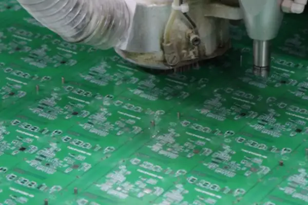
Once, during a visit to an electronics factory, I saw workers wearing magnifying glasses assembling micro-components in medical equipment. This level of precision is beyond the reach of the naked eye. It’s truly necessary for many factories to now use machine vision to inspect these minute flaws. For example, when inspecting circuit board solder joints, industrial cameras scan each joint with micron-level precision, using deep learning algorithms to identify more than twenty common defects such as cold solder joints and bridging. The inspection speed can reach thousands of solder joints per minute, a level of precision and efficiency that manual inspection simply cannot match.
I’ve noticed that even agricultural sensors are now using micro-circuit boards. The soil monitor I saw in the orchard last time used a specially designed waterproof circuit board. This application environment demands extremely high reliability—it must be resistant to both moisture and corrosion. These circuit boards typically use a polyimide substrate with a special conformal coating, capable of withstanding temperature variations from -40°C to 85°C. Even more impressively, they integrate solar charging modules and low-power wireless transmission capabilities, ensuring continuous operation for years in the field without battery replacement.
Actually, I think the most technologically demanding field is automotive electronics. The high-temperature environment in the engine compartment places stringent requirements on materials. I’ve seen a control board for a car camera that used a special ceramic substrate for heat dissipation. This ceramic substrate has a thermal conductivity more than ten times that of ordinary FR4 material, rapidly transferring heat generated by the chip to the metal casing. Furthermore, automotive electronics must meet automotive-grade reliability standards, such as stable operation in extreme temperatures ranging from -40°C to 125°C, and vibration testing across a frequency range of 10-2000Hz.
Many maker projects are now also starting to use custom-designed miniature circuit boards. Last week, I saw an environmental monitoring device made by a university student that used a self-designed micro-motherboard. This trend towards personalization may lead to more innovative applications. Thanks to open-source EDA design software and prototyping services, individual developers can customize professional-grade 4-6 layer circuit boards for a few hundred yuan. Some makers are even starting to experiment with flexible circuit board design, weaving sensors directly into clothing to create smart wearable devices.
The development direction of medical devices is also very interesting. Implantable devices require not only miniaturization but also biocompatibility. The R&D threshold for circuit boards for these special applications is indeed very high. For example, the circuit board for a pacemaker must use biocompatible titanium alloy packaging, all components must use lead-free solder, and it must pass rigorous biosafety testing. Even more complex is the need for extremely low power consumption design; a single button battery must be able to maintain a lifespan of 5-10 years.
Sometimes I wonder what these technological advancements really mean—perhaps it’s not just about making devices smaller and thinner, but about opening up new application scenarios! Like, if wireless headphones still used circuit board technology from twenty years ago, we’d probably still be dragging around a wire to listen to music! The tiny motherboard, about the size of a fingernail, inside today’s true wireless earbuds integrates not only Bluetooth chips and audio decoders, but also active noise cancellation processors and bone conduction sensors. This level of integration was unimaginable just ten years ago. Miniaturization technology is enabling emerging applications such as wearable devices, IoT sensors, and implantable medical devices, which may be the true meaning of technological development.
Recently, while disassembling an old hearing aid to study its internal structure, I discovered an interesting phenomenon: those tiny electronic components were neatly arranged on a circuit board the size of a fingernail. This trend of miniaturization has already permeated every corner of our lives—from the smartwatch on your wrist that tracks your heartbeat to the touch module hidden in your car’s steering wheel.
I remember once visiting a medical device exhibition and seeing a cross-sectional model of an endoscopic imaging probe. The doctor pointed to the metal tube, thinner than a ballpoint pen refill, and said that fitting an image sensor and LED strip inside was like doing micro-sculpture. What truly makes these components work together are those stacked micro-circuit boards that must ensure stable signal transmission and withstand repeated sterilization.
Car dashboards are increasingly resembling control panels from science fiction movies, but if you open the casing, you’ll find the real magic lies within those palm-sized circuit boards. My neighbor, who recently modified his car audio system, unearthed a motherboard smaller than a cigarette pack, yet it integrated audio processing, Bluetooth modules, and voice recognition.
Wearable devices have taken miniaturization to the extreme. My sports watch has a processor performance equivalent to a ten-year-old desktop computer, but its motherboard is smaller than a postage stamp. Engineers have managed to compress a gyroscope, heart rate sensor, and wireless charging coil all into this tiny cube. Sometimes when I wear it while running, I get dizzy—can this thing really monitor my blood oxygen data in real time?
But what surprises me most is that even drones are now the size of a playing card. Last time I saw someone fly a mini drone in the park; that tiny thing that took off and landed in the palm of my hand was equipped with a high-definition camera and obstacle avoidance system. After researching it, I discovered that its flight control system was entirely integrated onto a chocolate-sized circuit board with nearly a hundred solder points densely packed on it.
This highly integrated design philosophy is changing the logic of product development. Previously, engineers focused on implementing functionality; now, they must first consider how to make the circuit board “breathe” within a limited space. It’s like playing Tetris—not only do you have to fit the pieces perfectly, but you also need to allow for heat dissipation and electromagnetic interference.
Interestingly, miniaturization hasn’t made repairs more difficult; instead, it has spurred modular design. Many smart home devices now use plug-and-play circuit boards. When my robot vacuum’s wheel motor malfunctioned, I simply ordered the corresponding module online and replaced it in ten minutes. This design thinking might be more meaningful than simply pursuing miniaturization—it maintains precision while leaving room for user modifications.
Looking at the disassembled hearing aid motherboard on my desk, I suddenly felt that our attitude towards technological products should also be updated. As circuit boards become increasingly like works of art, perhaps we should have less of an impulse to upgrade and more of a reverence for precision manufacturing. After all, behind every micro-component lies the wisdom of engineers pushing the limits of physics.
When it comes to mastering micro-circuit boards, I think many people might be focusing on the wrong things. Everyone loves to focus on the high-end testing equipment and technical parameters, but what truly fascinates me are the tiny details that are almost invisible to the naked eye.
I remember spending an entire afternoon staring at solder joints under a microscope when I first encountered Miniature Circuit Boards. Those connections, smaller than sesame seeds, displayed a wondrous metallic luster under the magnifying glass. Some might find this observation tedious, but I discovered that these minute details determine the fate of the entire board. Sometimes, a seemingly perfect circuit board suddenly malfunctions, and the root cause might be a tiny crack in a solder joint due to temperature changes.
Speaking of testing, I’ve found that many beginners easily fall into the trap of over-reliance on instruments. Impedance testing is certainly important, but developing an intuitive judgment of the circuit board is even more crucial. Just as an experienced chef can sense the heat without a thermometer, I prefer to first visually inspect the overall condition of the circuit board, then combine this with instrument data for a comprehensive assessment. This dual-verification approach often uncovers problems that are easily overlooked when relying solely on instruments.
Environmental adaptability is indeed a pain point for miniature circuit boards. I’ve handled numerous cases where boards that performed perfectly in the lab experienced frequent problems in real-world applications. Once, a customer reported that their equipment frequently restarted in a humid environment; after investigation, it was discovered that the circuit board had undergone minute electrochemical migration in a high-temperature, high-humidity environment. These kinds of problems are difficult to detect in routine testing; they require simulating real-world usage environments to be captured.
What I really want to emphasize is that we need to treat these precision components with reverence. They are like fine Swiss watches, where every part is crucial. Sometimes we focus too much on technical parameters and neglect overall coordination. An excellent microcircuit board not only meets all specifications, but more importantly, all components can coexist harmoniously. This requires designers to understand both the technology and have a holistic perspective.
Looking back at those failed cases, the problems often lie in the most basic aspects. It might be a few degrees of temperature control deviation during soldering, or impurities invisible to the naked eye left during cleaning. These seemingly insignificant details are magnified into fatal problems in the microscopic world. Therefore, I’ve made it a habit to repeatedly verify even the simplest operations; this rigorous attitude has helped us avoid many potential risks.
Ultimately, the world of microcircuits is like a never-ending, precise dance. Every component must work perfectly within a limited space; any slight mistake can cause the entire performance to fail. But it’s precisely this challenge that makes the work so captivating; the sense of accomplishment when you see your designed circuit board running stably under various harsh environments is indescribable.
I recently disassembled a tiny circuit board inside an old hearing aid and truly realized how advanced technology is today. The board was smaller than a fingernail, yet it crammed in over a dozen components, arranged in a dense, maze-like structure that could only be seen under a microscope. This miniaturized design reminded me of the bulky circuit boards I used to use when repairing radios; now, the same function can be compressed to one-tenth of its original size.
Many people think that smaller circuit boards are simpler, but anyone who has actually designed one knows it’s a nightmare. Last time I tried to make a control board for a smart flowerpot, I went through seven or eight revisions just for the wiring of the sensors and microcontroller. Those hair-thin traces, even a slight misalignment can cause signal crosstalk, not to mention the issues of heat dissipation and electromagnetic interference.
A friend of mine works in medical device R&D. Their team spent six months shrinking the circuit board of a blood glucose meter to the size of a coin. The layout of the key components was like playing 3D chess—ensuring precision while avoiding interference between components. The most troublesome part was the soldering process; the workers had to wear magnifying glasses, and the slightest mistake would ruin the entire board.
Now even toys are using microcircuit technology. My son’s somersaulting robot, when I took it apart, had a motherboard as thin as paper. This progress is certainly convenient, but repairing it is a nightmare. Last week, I wanted to replace a capacitor, and when I used a hot air gun, all three resistors next to it fell off.
However, this high-density integration is forcing innovation in the industry. Last year, at an electronics exhibition, I saw some companies using 3D printing technology to stack circuit layers, which may even revolutionize the concept of traditional circuit boards. It’s just that with this miniaturization trend, it’s becoming increasingly difficult for DIY enthusiasts to get started—after all, who has a laser drilling machine at home?
I’ve always found those miniature circuit boards particularly interesting. Although they look like just a small piece of plastic with a few metal wires, there’s a lot of intricacies behind them.
I remember once disassembling an old MP3 player; the motherboard inside was smaller than a fingernail. I wondered how so many functions could fit into such a small space. Later, after more exposure, I realized the key lies in the hair-thin wiring design. These traces often use a multi-layered stacked structure, with signal lines, power lines, and ground lines arranged in layers through precise calculations, like a three-dimensional transportation system where they don’t interfere with each other. Designers also need to consider impedance matching and signal integrity, especially in high-frequency applications, where even the slightest reflection or crosstalk can degrade system performance.
Speaking of substrate material selection, I think many people tend to overlook this point. The impact of different substrate materials on signal transmission is quite significant. Once, when I was repairing a friend’s drone, the flight stability noticeably decreased after switching to a different supplier’s substrate. The problem was only solved by reverting to the original material. For example, FR-4 is cheaper but has poorer high-frequency characteristics, while polyimide is more flexible but more expensive. In high-temperature environments, the difference in the coefficient of thermal expansion of different substrate materials can also affect the reliability of solder joints, which is a major reason why military-grade products often use special substrates.
Many electronic products are now pursuing thinner and lighter designs, which places higher demands on the miniaturization of circuit boards. However, I’ve noticed that sometimes manufacturers, in order to reduce size, overly dense wiring can cause problems with heat dissipation. Especially around power devices, overly dense wiring can hinder heat dissipation, leading to localized temperature increases. I once tested an ultra-thin phone whose motherboard temperature reached over 70 degrees Celsius after prolonged gaming, which not only affects battery life but may also cause premature aging of components.
I appreciate products that strike a balance between design and practicality. For example, the miniature circuit boards used in some medical devices ensure both precision and sufficient safety margins. This design approach is truly worth learning from. Take pacemakers as an example; their circuit boards must not only meet stringent electromagnetic compatibility standards but also consider biocompatibility and long-term reliability. Designers incorporate redundant circuits along critical signal paths and employ special coating processes to resist corrosion from bodily fluids.
In fact, after working in this field for a while, you’ll understand that good circuit board design isn’t just about miniaturization, but about considering the actual usage scenarios. After all, even the most ingenious design is useless if it doesn’t work. For instance, the shock resistance design of industrial control boards is much more stringent than that of consumer electronics, often requiring additional reinforcing ribs and fixing points. In the automotive electronics field, circuit boards must pass rigorous environmental tests, including high temperature and humidity, vibration and shock, to ensure stable operation under extreme conditions.
Recently, I’ve been trying to design a circuit board for a mini speaker. Although progress is slow, I feel a great sense of accomplishment each time I solve a small problem. Perhaps this is the charm of miniature circuit boards—showcasing the ingenuity of technology within a small space. For example, special attention must be paid to the isolation between analog and digital circuits during layout to avoid digital noise interfering with audio signals. Grounding is also a science; improper handling can introduce buzzing AC noise.
Sometimes, looking at those densely packed lines, I think of urban transportation networks. Although the scale differs, the core design principles are the same: ensuring efficiency while allowing for flexibility. Just as urban planning includes emergency lanes, circuit boards need test points and debugging interfaces. A clever designer will leave room for future upgrades without increasing costs, such as adding more unconnected pads for future functional expansion.
I believe the future development of microcircuits will increasingly focus on material innovation. After all, physical dimensions have limits, but advancements in materials bring more possibilities. For example, graphene substrates promise to reduce circuit thickness to the atomic level, while self-healing materials can automatically repair microcracks caused by stress. The development of flexible electronic materials is even more exciting; in the future, we may see foldable devices using circuit boards as flexible as paper.
However, no matter how technology changes, good design principles will never become outdated. As my teacher often says, even the most complex technology ultimately serves humanity. This reminds me of the joy I felt when I first successfully lit up an LED circuit I designed. That sense of satisfaction in transforming abstract principles into practical works is the fundamental driving force behind technological development.
In the field of industrial automation, people often pay attention to AI
Ever wonder how your phone maintains a stable signal? It relies on
When selecting components for a security monitoring system, most attention goes to
- Эксперт в области мелко- и среднесерийного производства
- Высокоточное изготовление печатных плат и автоматизированная сборка
- Надежный партнер для электронных проектов OEM/ODM
Часы работы: (пн-сб) с 9:00 до 18:30