
Industrial Automation PCB Reliability: How to Achieve 10+ Years of Stable Operation
In the field of industrial automation, people often pay attention to AI
I’ve seen many people focus excessively on price when choosing a PCB assembly manufacturer, neglecting the most fundamental aspects. In fact, what truly determines the success or failure of a product is often not the flashy added services, but the supplier’s ability to control basic processes. Take placement accuracy, for example. Some factories relax standards to meet deadlines, resulting in bridging or cold solder joints during mass production. This problem might not be obvious in the prototype stage, but it will trigger a chain reaction like a domino effect during mass production.
I remember a friend who works on industrial control boards complaining last year that they switched to a cheaper PCB assembly supplier, and 30% of their first batch of 500 products had capacitors with reversed polarity. The rework costs directly wiped out the savings and delayed the project. This case perfectly illustrates a point: in the field of electronics manufacturing, seemingly simple processes are often the most challenging. For example, when performing secondary reflow soldering on a double-sided board, if the temperature profile is set incorrectly, the ball grid array package at the bottom will shift. This kind of hidden problem may not even be detected during the testing phase.
Many PCB assembly factories now like to advertise how many high-end pieces of equipment they have, but what’s truly crucial is the engineers’ understanding of material properties. Why do some factories achieve a yield rate of over 99.9% for component placement? The secret lies in their ability to adjust the stencil opening ratio based on different brands of solder paste and even calibrate the thermal expansion coefficient for each batch of PCB boards. This meticulous attention to detail is what truly sets companies apart.
I particularly appreciate suppliers who are willing to invest time in process validation. They don’t rush to give you a delivery date; instead, they spend a couple of days conducting design for manufacturability analysis. Once, we had a circuit board that required a mix of through-hole connectors and miniature BGAs. The factory we were working with suggested rotating the layout of certain components by 15 degrees. This seemingly minor adjustment optimized the pick-and-place machine’s nozzle path by 40%, significantly reducing the defect rate.
Ultimately, choosing a PCBA partner is like choosing a surgeon; simply looking at the clinic’s decor isn’t enough. You need to consider their experience in handling complex problems. Be wary of those who constantly say “no problem,” because electronic manufacturing is fundamentally a process of continuously solving problems.
I’ve always found the process of choosing a PCB assembly manufacturer quite interesting. Many people think finding a supplier is as simple as comparing prices and delivery times. However, you only realize that details determine success or failure once you actually start working together.
I remember one project where we were in a hurry to launch, but we discovered several cold solder joints during testing. The entire team was frantic. Fortunately, our PCB assembly supplier reacted very quickly. They sent an engineer with a portable microscope to analyze the solder joints on-site. Within two hours, they identified the problem: an issue with the solder paste activity in a particular batch. This kind of problem is impossible to detect with automated testing equipment; it requires the experience of a skilled technician.
Many manufacturers now focus on production speed, but I value their repair capabilities more. After all, electronic components are becoming increasingly precise. For chips like BGAs, if something goes wrong, you can’t fix it without a professional rework station. Once, I visited a partner’s rework workshop and saw an engineer operating a rework station with infrared heating; it was like performing delicate surgery, with precise temperature control and zoned heating—even more meticulous than replacing a phone screen.
The testing phase is also very complex. I’ve seen some small factories treat AOI scanning as a magic bullet. However, for boards with double-sided surface mounting, optical inspection can only see the surface; the real problems are hidden in the concealed solder joints. The factory we currently work with proactively suggests adding AXI testing at critical points. Although it’s a bit more expensive, it avoids costly rework later. Suppliers who think proactively like this are the ones worth working with long-term. What impressed me most was a functional test where we discovered the board was unstable in low-temperature environments. A typical PCBA manufacturer might have suggested we loosen the technical parameters, but that supplier worked with us for two consecutive nights, adjusting the component layout and ultimately solving the problem by improving the heat dissipation path. This dedication to detail is the most valuable quality in manufacturing.
Ultimately, choosing a PCB assembly supplier is like choosing a partner. Technology and equipment are fundamental, but the real difference lies in how they handle problems. Manufacturers willing to invest extra effort in your project, even if their quote is slightly higher, can save you more in hidden costs in the long run.
Every time I see complex circuit board designs, I’m reminded of a project I helped a friend’s company with last year. The PCB assembly manufacturer they chose had problems with the soldering process, resulting in the entire batch of products needing rework. This made me realize that choosing the right partner is far more important than simply comparing prices.
Many companies now treat PCBA as a standard commodity. However, each project has unique requirements. Some require special packaging processes, while others have particularly high demands on heat dissipation. A good PCB assembly supplier will take the time to understand your product’s application scenario. For example, in the automotive electronics field, suppliers need to understand the special requirements of vibration environments on solder joint reliability, which directly affects the product’s lifespan under extreme conditions.
The most reliable collaboration I’ve seen was with a company that manufactures medical equipment. Their PCB assembly partner not only provided standard services but also proactively suggested improvements. For example, for equipment used in humid environments, they adjusted process parameters to enhance moisture resistance. This deep collaboration improved the reliability of the final product significantly.
Sometimes, smaller companies can offer more flexible services. Last week, I contacted a manufacturer specializing in high-end packaging, and they could complete sample production within 48 hours. This responsiveness is a lifesaver for projects with tight development cycles. Especially when the design requires multiple iterations, rapid prototyping helps engineers verify design assumptions in a timely manner.
When choosing a long-term PCB assembly manufacturer, I particularly value their process stability. I once visited a factory’s production line and found that they calibrated their equipment parameters daily. This attention to detail directly affects the yield rate. For example, a 0.5-degree deviation in the reflow soldering oven’s temperature curve can lead to poor soldering, while strict daily calibration ensures consistent quality for every batch of products.
With the rapid iteration of new technologies, a simple OEM relationship is no longer sufficient. An ideal partner should be able to jointly address technological challenges. For example, the recently popular heterogeneous integration technology requires manufacturers to possess multi-material processing capabilities. This requires suppliers to not only handle traditional FR-4 boards but also be familiar with the processing characteristics of special materials such as ceramic substrates and flexible circuits.
What I appreciate most are suppliers who are willing to share their experience. They don’t keep process parameters a secret, but instead explain why a particular method is used in a certain step. This transparency builds genuine trust. For example, one supplier explained in detail the reasons for choosing a specific solder paste ratio, which helped us optimize component layout.
Ultimately, good PCB assembly collaboration is like a jigsaw puzzle. Both sides contribute their expertise to complete the picture. The manufacturer contributes process experience, and the designer provides product insights. This complementary relationship often produces a result greater than the sum of its parts. For example, the manufacturer suggested rotating the BGA chip by 45 degrees, which improved both wiring efficiency and heat dissipation.
I remember once, to meet a tight deadline, we tried using multiple suppliers to produce different batches. However, differences in processes led to product inconsistency. This lesson taught me the value of concentrated collaboration. Instead of spreading the risk, it’s better to cultivate a deep partnership with reliable partners. Deep collaboration allows suppliers to become more familiar with our quality standards and design practices.
Every time I review a new product design, I think about whether the design considers manufacturing feasibility. Sometimes, a slight adjustment to a component layout can significantly reduce assembly difficulty. This design-for-manufacturing mindset is becoming the new normal in the industry. For example, increasing the spacing between adjacent components by 0.2 millimeters might increase the placement success rate of the automatic pick-and-place machine from 95% to 99.5%.
I’ve seen many people fall into a trap when choosing PCB assembly manufacturers – focusing too much on the certificates hanging on the wall. Of course, ISO certification is important, but it’s just a ticket to entry. What truly determines the quality of the collaboration is often the things you can’t see behind those certificates.
I remember last year we had a medical device project. We compared three PCB assembly suppliers, all with ISO 13485 certification. The first one we visited had an immaculate workshop, but the engineers’ suggestions on heat dissipation design were purely theoretical. The second one had slightly older equipment, but the process manager directly pointed out several layout issues that could cause micro-shorts and shared examples of how they had improved similar problems before. This practical experience is invaluable. This is especially true in the automotive electronics field, where IATF16949 is practically standard. But what truly reassures me are the manufacturers who proactively display SPC data curves. They not only tell you that they meet the standards but also explain why a certain temperature parameter range needs to be controlled within plus or minus three degrees. This attention to detail is far more reliable than simply attaching a label.
A good PCB assembly process should be dynamically adjusted. I’ve found that excellent manufacturers never treat process standards as immutable dogma. They fine-tune solder paste ratios and reflow soldering curves based on board material characteristics, component batches, and even seasonal humidity changes. This flexibility often guarantees the long-term reliability of the PCBA better than rigidly adhering to specifications.
In fact, there’s a simple way to judge whether a manufacturer is reliable: see if they are willing to share failure cases. I recently encountered a military-grade PCB assembly manufacturer who openly analyzed the impedance deviation problem during the first trial production of a high-frequency module and how they subsequently solved it by adjusting the layer structure. This transparency and problem-solving attitude are more reassuring than any certification.
Ultimately, choosing a partner is like choosing a spouse; looking at their resume isn’t enough. You need to see their first reaction when problems arise – do they shirk responsibility or work together to solve them? Teams that internalize industry standards into their daily practices are often the ones who can go the distance with you.
I recently chatted with a friend who works in smart hardware, and he mentioned encountering many pitfalls when finding PCB assembly suppliers. Many people still think of PCBA as simply “soldering the parts on,” which reminds me of my own thinking when I first entered this industry five years ago.
Back then, I thought PCB assembly was just a matter of finding a contract manufacturer. Later, I realized that different manufacturers have vastly different levels of control over process details. Once, our product batch had a problem with cold solder joints, and we traced it back to a PCB assembly manufacturer who had adjusted the solder paste formula to save costs. This seemingly minor change directly resulted in the entire batch needing rework.
Now, when choosing a PCBA partner, I pay more attention to how they handle unconventional requirements. For example, we recently needed to mount miniature sensors on a flexible circuit board. Most suppliers said they needed special fixtures. But one manufacturer suggested using a semi-automatic mounting process with manual inspection, which not only shortened the lead time but also saved 30% of the cost. This ability to adapt flexibly is the core competitiveness of modern electronics manufacturing.
I particularly value communication efficiency during the assembly process. I’ve worked with suppliers who require email confirmation for every single step, and I’ve also collaborated with teams that provide real-time production progress updates. While the latter’s quotes were slightly higher, they consistently delivered urgent orders ahead of schedule, ultimately saving us money. Now, I believe that PCBA quality depends not only on the fullness and neatness of the solder joints but also on the smoothness and transparency of the entire collaboration process.
Recently, I’ve observed an interesting trend: many small and medium-sized PCB assembly manufacturers are starting to focus on niche markets. One factory specializing in medical equipment PCBA even strictly controls the temperature and humidity in its workshops. Although their SMT lines aren’t the most advanced, their yield rate is actually higher than that of larger manufacturers. This strategy of focusing on specific areas might be more worthwhile than blindly pursuing equipment upgrades.
There’s a simple way to determine if a PCB assembly supplier is reliable: see if they allow you to visit their production line at any time. Manufacturers willing to open up their production process usually have more confidence in their craftsmanship, while those who always use “trade secrets” as an excuse should be viewed with caution. After all, true core technology should be reflected in a stable yield rate, not in secrecy.
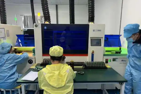
After interacting with many PCB assembly manufacturers, I’ve found that what truly determines PCBA quality is not how advanced the equipment is, but the degree of control over process details. Once, during a factory visit, I saw them using a microscope to inspect solder joint morphology. That level of dedication made me realize that excellent PCB assembly suppliers treat each connection point as a work of art. For example, they’ve established a database of solder joint morphology, quantitatively comparing the ideal solder joint profiles of different components. This standardized operation effectively avoids human judgment errors. Especially in high-reliability fields like medical or aerospace, they even perform cross-sectional analysis of solder joints to detect the formation of intermetallic compounds.
Packaging technology has changed rapidly in recent years, from traditional QFP to the current BGA, and the requirements for placement accuracy have increased exponentially. I’ve seen cases where a 0.5% deviation in solder alloy composition led to the failure of an entire batch of products during thermal cycling tests. This reminds me of playing jigsaw puzzles as a child – a seemingly small misalignment can make the whole picture look wrong. Now, even more advanced CSP packaging controls solder ball diameter to within 0.2mm, requiring real-time monitoring of substrate warping and deformation during placement, which places extremely high demands on the equipment’s thermal compensation system. Some manufacturers even use X-ray inspection to check the void rate of BGA solder joints, ensuring that every hidden solder joint meets the standard.
Many people think that soldering is simply about heating and melting, but controlling the temperature curve is actually a very demanding process that requires considerable experience. It’s like baking a cake; the same ingredients will produce vastly different results depending on the baking temperature. I once saw an engineer adjust the reflow soldering curve for a specific component, testing it more than ten times before determining the optimal parameters. This kind of attention to detail is the attitude that truly trustworthy PCB assembly manufacturers should have. They even consider the differences in heat absorption of components of different colors; darker components require a slightly lower preheating temperature. This subtle adjustment often prevents component cracking or the “popcorn” effect.
Now, some manufacturers use cheap solder to reduce costs, resulting in products that develop poor solder joints after only six months. In one project I worked on, we insisted on using silver-containing solder paste, which increased costs by 15%, but reduced the repair rate by 80% over three years. This long-term benefit is often overlooked by short-term cost calculations. High-quality solder paste has better oxidation resistance and maintains a longer usable lifespan after opening, thus reducing material waste. Some automotive electronics manufacturers even require solder suppliers to provide trace element analysis reports for each batch.
Recently, I’ve encountered an interesting phenomenon: some customers are starting to request video recordings of the soldering process. This is a great idea – making the process transparent has become a new competitive advantage. After all, when you can clearly demonstrate the placement angle of each component and the solder wetting status, customers will naturally trust your PCB assembly capabilities. This video data can also be used for AI analysis, employing machine learning to identify abnormal soldering patterns, such as early signs of component misalignment or solder splashing, enabling preventative quality control.
Speaking of packaging density, some designs are truly pushing the limits. Last time I saw a fingernail-sized area with over twenty components, even the cleaning agent flow rate had to be recalculated. This high-density assembly is like assembling gears in a watch; the precision of every step must be perfectly matched. Now, 01005 size components are commonplace, and some manufacturers are starting to experiment with 008004 specifications. These components, smaller than a grain of salt, require specially designed nozzles, and even the electrostatic discharge (ESD) protection level in the workshop needs to be upgraded to Level 1.
What impresses me most is the speed of technological iteration in this industry. Processes that were considered advanced five years ago may now be outdated; equipment that seemed precise enough two years ago is now insufficient; when choosing a PCB assembly partner, you really need to consider whether they have a continuous improvement mindset. After all, the lifecycle of electronic products is getting shorter and shorter, and if manufacturing processes can’t keep up, they will quickly become obsolete. Leading factories are now deploying digital twin technology, simulating the entire production line in a virtual environment to optimize process parameters in advance. While this forward-looking investment may not show returns in the short term, it ensures technological competitiveness for the next three to five years.
Whenever I talk to colleagues about finding a PCB assembly manufacturer, I always feel that people easily fall into a trap—thinking that everything is fine as long as the supplier can provide X-ray inspection reports or solderability test data. In fact, what truly determines PCBA quality are often those invisible details. I remember last year we used a new supplier for a project; their inspection documents were more comprehensive than a textbook, but the first batch of boards had widespread defective soldering. Later, we discovered that the problem wasn’t with the testing equipment at all, but that their materials handler had mixed components from different batches.
Now, when I discuss cooperation with PCB assembly suppliers, I pay more attention to their warehouse management processes. For example, whether components are sorted by batch when they are put on the shelves, and whether there is a double-checking mechanism in the material dispensing process. These seemingly basic operations often reflect the true level of management more accurately than expensive testing equipment. After all, even the most advanced X-ray machine can’t detect flaws in the material traceability chain.
Speaking of component quality control, I think there’s a particularly interesting phenomenon in the industry. Many manufacturers are keen to showcase their original manufacturer authorization certificates from top distributors, but when a material shortage crisis actually hits, what’s truly tested is the procurement team’s resourcefulness. During the worst of the chip shortage, the manufacturer we’ve worked with the longest performed the most steadily – their procurement director regularly went to Huaqiangbei in Shenzhen, chatting and having tea with the stall owners. This seemingly unconventional channel, at critical moments, allowed them to gauge the real inventory levels in the market.
Recently, I’ve been reflecting on a question: are we too fixated on quantitative indicators when evaluating PCB assembly quality? For example, we focus excessively on yield rates, but neglect whether the temperature and humidity logs on the production line are being properly filled out. Once, when visiting a factory, I found that their solder paste tempering time was controlled even more strictly than military specifications, but the employees habitually wore ordinary cotton gloves when handling the boards. These contradictions in details often reveal the true management culture.
In fact, choosing a partner is like choosing fruit; only looking at test certificates is as one-sided as only checking the sugar content of the fruit. Truly experienced buyers observe the freshness of the stem and feel the elasticity of the peel – in the PCB assembly field, this might correspond to checking whether their material racks are color-coded by status, or whether engineers habitually clean the soldering iron tip when debugging equipment. These subconscious actions reveal a company’s quality DNA.
In the field of industrial automation, people often pay attention to AI
Ever wonder how your phone maintains a stable signal? It relies on
When selecting components for a security monitoring system, most attention goes to
- Эксперт в области мелко- и среднесерийного производства
- Высокоточное изготовление печатных плат и автоматизированная сборка
- Надежный партнер для электронных проектов OEM/ODM
Часы работы: (пн-сб) с 9:00 до 18:30