

Why the Best PCB Supply Chains Are Built Like Relationships, Not Transactions: Lessons for Satellite Communication PCB Programs
What actually makes a long-term PCB supply chain partnership work — shared
The Sharp Corner That Melted a Board
When I first started working on high-current PCB assembly, I made plenty of mistakes. Back then, I assumed that as long as the traces were connected, it would work. Our first batch of boards came back and started smoking the moment we powered them on. It took time to gradually understand that dealing with high power density is an entirely different game.
You have to think about how current actually travels. It’s not a simple connectivity question. When current is large, it finds its own path. Sometimes you think you’ve designed the path correctly, but once powered on, current might travel through a spot you never anticipated. That creates hot spots, or even burns through the board. I saw a case where a designer left a small sharp corner on the board without noticing. When high current passed through, the temperature there spiked, and it melted straight through the copper foil. In reality, current in a conductor tends to flow along the path of least impedance, and there’s a skin effect — at high frequency, current concentrates more toward the surface. A sharp corner or bottleneck sharply increases current density, and localized Joule heating grows with the square of current density, far exceeding the average temperature rise.
Thermal management is a part that’s especially easy to overlook. Many people think adding a heatsink is enough. It’s really not that simple. Heat has to travel from inside the chip to the case, and then to the heatsink — every link along that path adds resistance. Poor solder quality or an uneven contact surface can dramatically increase thermal resistance. A chip’s surface temperature might look normal while its internal junction temperature has already exceeded limits. For example, a power MOSFET has a fixed junction-to-case thermal resistance (RθJC), but if poor-quality thermal paste is used, or improper mounting torque causes excessive contact thermal resistance (RθCS), the chip’s core can still be damaged by heat buildup even if the heatsink itself stays cool. Thermal simulation often only looks at the macro picture, missing these micro-level interface issues.
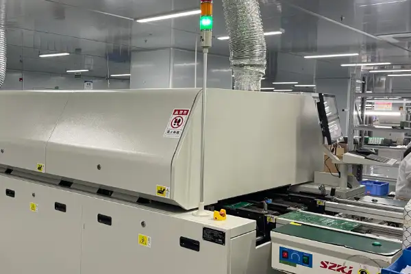
On the topic of power conversion board assembly process, I think a lot of people rely too heavily on theoretical calculation. Calculation matters, of course, but there are too many variables in actual assembly. For instance, if the soldering temperature profile isn’t well controlled, it can cause cold joints or solder voids. This might not be noticeable on a low-power board, but in a high-current application, it’s a fatal problem. Current concentrates in the parts that are properly soldered, causing localized overheating. For example, during reflow soldering, if peak temperature is insufficient or time above liquidus is too short, the solder and pad may fail to form a proper intermetallic compound layer — the connection is essentially mechanical rather than electrical, and its resistance can be dozens of times that of a good solder joint.
On the topic of safety standards, I think many teams today don’t do enough. It’s not just about passing certification. What genuinely matters is understanding the principles behind those standards — why they’re written that way. Take creepage distance requirements, for example — they’re not just there to pass a test, but to prevent unexpected discharge in humid or dusty environments. I’ve seen a product pass lab testing fine, but in actual use, dust accumulation caused a short circuit. Creepage distance design needs to account for the material’s Comparative Tracking Index (CTI); in industrial environments with a higher pollution degree, even tiny conductive contaminants accumulating along the surface can form a leakage path across an otherwise safe clearance, causing fire or electric shock.
Material selection is often underestimated. Different board materials perform very differently at high frequency, especially PCBs in switching power supply applications, where ordinary FR4 material has significant loss at high frequency, leading to reduced efficiency and increased heat. Sometimes spending a bit more on better board material actually saves on thermal management costs. Take a common switching power supply operating in the hundreds of kHz range as an example — FR4’s dielectric loss factor (Df) is relatively high, and its dielectric loss converts to heat, potentially affecting signal integrity too. Using a high-frequency, low-loss material like Rogers or Panasonic MEGTRON, while costing more upfront, can improve efficiency, reduce temperature rise, and improve reliability — potentially more economical when viewed across the full lifecycle.
On testing, many people only run functional tests and skip stress testing, especially thermal cycling tests. After a board goes through a few hot-cold cycles, some solder joints develop cracks — cracks you can’t see under normal conditions, but that increase resistance under high current, causing localized overheating and eventual failure. A good power PCBA should be able to withstand the temperature swings of actual use. This is because the PCB, components, and solder have different coefficients of thermal expansion (CTE), and temperature cycling generates mechanical stress — lead-free solder in particular is quite brittle. For example, a cycling test from -40°C to 125°C effectively exposes this kind of latent defect, while functional testing at room temperature cannot reveal it.
I think what this line of work needs most is patience and accumulated experience. Every project runs into new problems, and there’s no one-size-fits-all solution. The key is to keep hands-on, keep testing, and record every problem and its solution as it comes up. Over time, you build your own judgment — knowing which spots are prone to problems and need special attention. That matters more than any theory. For example, how to lay out a board so the high-current path is shortest and loop area smallest, how to balance copper thickness, trace width, and temperature rise — this kind of intuition usually comes from accumulating both failures and successes.
Looking back now at those burned boards, it hurt at the time, but I genuinely learned a lot from them.
Why Blanket Copper Thickness Isn’t the Answer
I’ve always felt that a lot of people misunderstand how to handle high current on a PCB. Everyone assumes that simply thickening and widening the traces solves the problem. In reality, working on Power Conversion PCB Assembly, I’ve run into plenty of issues that prove otherwise.
Once, I got a board that looked pretty solid — it used very thick copper layers — but actual testing showed the temperature rise was surprisingly fast. It later turned out the problem was in the layout, not simply insufficient copper thickness. The current path was designed with unnecessary twists and turns, and local impedance was still too high.
On copper thickness selection, I think you need a more flexible view. Not every location needs uniform thickening — that sends cost skyrocketing and significantly increases manufacturing difficulty. My current approach is to locally increase copper thickness only on the critical high-current paths, keeping conventional thickness elsewhere — this controls cost while ensuring performance.
Actually, many people overlook the PCB’s own thermal dissipation capability. In high-density assembly, heat accumulates in certain regions — if you only increase copper thickness without considering thermal pathways, the effect can backfire. I’ve seen designs that fill the area around power devices with vias to help conduct heat to the back side — this approach is more meaningful than simply piling on copper.
Material selection is another critical factor. Ordinary FR4 material shows noticeable loss under high-frequency, high-current conditions. Sometimes switching to a better substrate material is more effective than simply increasing copper thickness — though this obviously needs to be balanced against cost.
In actual practice, I’ve found that many engineers’ understanding of High Current PCBA still stays at the theoretical level — for example, calculating trace width from a standard table and leaving margin for maximum current. But in reality, ambient temperature, airflow conditions, and thermal radiation from adjacent components all affect the final outcome. I recommend leaving enough testing time to simulate real-world usage conditions when doing this kind of design.
I remember a project involving a motor drive board. Early on, we followed standard practice and used 2-ounce copper, but during sustained full-load testing, overheating still occurred. We later adjusted the layout, shortening the high-current path by a third, and the problem was solved. This shows that pure physical parameters alone can’t solve every problem.
Many new power devices today are operating at increasingly higher frequencies, which is changing PCB requirements — traditional design experience may need updating. GaN devices, for example, switch extremely fast and are very sensitive to loop inductance — in this case, the copper layer’s thickness and shape affect parasitic parameters, details that are easy to overlook.
I think what power electronics work needs most is systems thinking. You can’t just look at a single parameter — copper thickness matters, sure, but it’s only one link in the entire energy conversion system. You also need to consider connector current-carrying capacity, solder joint reliability, even wire selection, and more.
Every time I see someone fixating on a single PCB parameter, I want to remind them to look at the overall effect — after all, the final product needs to work reliably in a real-world environment, not just satisfy the numbers on a design spec sheet.
Why Etching Precision Beats Simply Adding More Copper
I once worked on a project that required routing very large current on a fairly small board. At first, I also thought thickening the copper foil would solve the problem. But once I actually started working on it, I found things weren’t that simple.
Once you make the copper foil too thick, problems arise. The etching process becomes hard to control, and trace edges can become rough or even develop notches. The safety clearance you originally designed can be compromised by this kind of lateral etching, significantly increasing short-circuit risk — which is fatal in a high-current application.
The board material itself is also a challenge. Ordinary FR4 material’s performance degrades under the combined pressure of high voltage and high current, especially if its tracking resistance capability — its CTI value — isn’t high enough, causing insulation performance to decline over long-term operation. I later found that choosing a specialized board material with a higher CTI value, while raising cost, delivers a more reliable creepage distance design, and the board can actually be made more compact.
On carrying high current, many people’s first instinct is to desperately widen the traces or stack many layers, but that’s often not the optimal solution. My experience is that when doing PCB assembly for power conversion, you need a different approach — don’t just fixate on the PCB’s own routing.
Sometimes, rather than racking your brain over the internal board layout, it’s worth considering an external solution — for example, reserving a spot on the PCB to solder solid copper bars or copper blocks directly, letting the main current travel through these low-impedance paths. This dramatically reduces the burden on the PCB’s internal traces, and temperature rise becomes much easier to control.
I’ve also tried a hybrid structural design approach — treating the power layer carrying high current and the signal layer carrying control lines separately, using different copper foil thicknesses. The power section can use 2 or even 3 ounces, while the signal section uses standard 1 ounce — this ensures current-carrying capacity without making the entire board’s process overly complex and expensive.
Ultimately, designing a circuit board that can handle high-current challenges is more like a systemic balancing act — you need to find the optimal combination point among electrical performance, process feasibility, and cost. Blindly chasing a single metric often ruins the whole thing.
What genuinely matters is understanding how current actually flows, which paths are bottlenecks, and then addressing them in a targeted way — maybe by optimizing layout, maybe by selecting special materials, maybe by introducing auxiliary structures. There’s no fixed answer — every time is a new challenge.
Why the Solder Joint Matters More Than the Board Material
Every time I look at complex power conversion boards, I find them genuinely interesting. Many people jump straight into thinking about which premium board material to use, or how to add slots to increase creepage distance. I think that’s a bit backwards. What actually determines whether a board can withstand high voltage and high current usually isn’t the most expensive material — it’s the most basic thing: the solder joint.
I’ve seen too many examples where things went wrong because of poor package-to-pad matching on the PCB, especially in High Current PCBA work, where the problem is especially pronounced. You select a power MOSFET with beautiful-looking parameters — say, a TO-247 package — thinking it has great thermal performance. Then you draw the layout directly following the datasheet’s recommended oversized pad dimensions. The result? The board comes back from reflow, and that big component is tilted or lifted, because the uneven surface tension of the molten solder paste pushed it askew. At that point, no matter how high your board material’s CTI value, or how perfectly designed your creepage slots, none of it matters. A cold joint or a stress-affected connection is the weakest link under long-term high-current stress — sooner or later, it will fail.
So now, when handling this kind of Power Conversion PCB Assembly project, the first step for me is actually not looking at board material specs. I’ll sit down with the manufacturing plant’s engineers first, to see what experience-based recommendations they have for stencil aperture design for that kind of oversized pad. Often, splitting a single large copper area into several smaller regions with gaps in between, or opening the stencil in a corresponding mesh pattern, effectively resolves the floating and gas-entrapment problems during soldering. Doesn’t that sound far more practical than simply switching to a more expensive substrate material?
On the topic of wide-bandgap devices, like the now-popular GaN and SiC, their layout requirements are genuinely demanding, but I think the assembly-stage challenges are underestimated. These devices switch at frighteningly fast speeds, so everyone focuses heavily on optimizing routing to reduce parasitic inductance — that’s correct, but if that tiny chip can’t even be soldered onto the board stably, everything else is moot.
Their packages keep getting smaller and thinner, and some solder ball pitches are as fine as flour grains — this places nearly stringent demands on solder paste printing precision and reflow temperature profile. Even a small deviation can cause tombstoning or bridging.
Sometimes I wonder if we’re too obsessed with the performance gains from new devices and new materials, and end up overlooking some fundamental but critical process details. A reliable power board has always been a systems engineering effort — from chip selection, package matching, to PCB design, and finally assembly and soldering — every link needs to be solid. Pouring cost aggressively into just one point can backfire.
Solder Joints, Loop Geometry, and Vibration: Three Overlooked Structural Failures
I’ve recently noticed an interesting phenomenon: many engineers, when designing high-power circuit boards, pay very close attention to switching transistor selection and processing details — handled quite thoroughly — yet often overlook the importance of seemingly minor connection points and support structures.
Take a high-current power module we worked on. At the time, chasing extreme efficiency targets, we selected a very high-performing wide-bandgap semiconductor device, and the entire power conversion section’s layout was optimized repeatedly. In theory, there shouldn’t have been any problems, but actual testing kept showing mysterious voltage glitches.
We later shifted our attention away from the chip itself and carefully examined the copper traces serving the power path on the PCB, finding the problem in a very basic place: the physical shape of the current loop wasn’t compact enough, causing parasitic parameters to exceed expectations. Specifically, that critical high-frequency current loop’s area was too large, forming an invisible “antenna” — not only introducing extra distributed inductance, causing voltage overshoot at switching instants, but also making it easier to couple external electromagnetic interference. This loop was inadvertently formed by the placement of the switching transistor, inductor, and input/output capacitors. Simply optimizing the routing of a single component, without examining the physical layout of the entire loop, cannot fundamentally suppress this noise.
This reminds me of a car charger board I worked on before, which used a fairly bulky, heavy energy-storage inductor. At first, we thought soldering it securely was enough. It turned out that in vibration testing, tiny cracks appeared around the solder joints before long.
Actually, this kind of magnetic component generates its own heat during operation, and combined with thermal expansion and contraction from external environmental temperature changes, the internal structure of the solder can indeed change over time. Especially in dynamic environments like vehicle start-stop cycles or bumpy roads, the component’s own mass generates continuous inertial force, all borne by a few solder pads — their metal fatigue accelerates.
So now, when we run into similar situations, we recommend that clients, beyond ensuring solder quality, also mechanically secure the component body — for example, adding a bracket or using adhesive for reinforcement. Though it looks like a small change, it has a very noticeable effect on improving overall reliability. For example, using high-strength silicone for underfill or side reinforcement both cushions vibration stress and allows some thermal deformation — far more reliable than relying on solder joints alone.
Another commonly overlooked point is CTE matching between different materials. When current is large, copper foil temperature rises noticeably — if its thermal characteristics differ too much from the substrate material, repeated thermal cycling can cause copper foil delamination or even cracking. Copper’s CTE is about 17 ppm/°C, while ordinary FR4 substrate’s Z-axis (thickness direction) CTE can be as high as 70-80 ppm/°C — this mismatch generates enormous interlayer shear stress during dramatic temperature swings.
I’ve seen some high-density power boards that, to control cost, used ordinary FR4 material, and after temperature rose in the high-current area, the substrate showed slight deformation — not enough to cause immediate failure, but certainly affecting lifespan long-term. This deformation subtly changes the relative position and stress distribution between components, and might even create gaps in an originally well-mated heatsink, increasing thermal resistance and forming a vicious cycle.
Of course, these problems aren’t unsolvable — for instance, you can consider using metal-core or ceramic substrates in critical areas. While cost goes up, for applications with extremely high reliability requirements, that investment is worth it. Metal-core substrates (like aluminum-core) offer excellent thermal conductivity, quickly equalizing temperature, and match copper foil’s CTE better; ceramic substrates (like alumina or aluminum nitride) offer excellent insulation and thermal stability, well-suited for ultra-high-frequency or ultra-high-power-density applications.
Additionally, spending more time on simulation analysis during the design stage is very helpful — not just circuit performance simulation, but also thermal analysis and mechanical stress analysis. Many software tools today can provide fairly accurate predictions. Thermal simulation can identify localized overheating “hot spots” in advance, allowing layout adjustment or enhanced cooling; mechanical simulation can model a board’s deformation and stress concentration under vibration and shock, guiding the placement of reinforcement ribs or fixing points.
Sometimes we’re too focused on optimizing a single metric to its extreme, overlooking the importance of overall system coordination. A truly reliable power conversion circuit board needs a good balance among electrical performance, thermal management, and mechanical structure.
It’s like building with blocks — every piece needs to go in the right place, and they need to fit tightly together, to build something tall and stable.
Thermal Flow Mapping Before Component Placement
I’ve always felt that a lot of people overcomplicate power design. Every time I see discussions about high-power-density power supplies filled with jargon and technical parameters, I want to laugh. It’s as if you’re not professional enough unless you throw around a few specialized terms.
Actually, doing Power Conversion PCB Assembly, especially handling High Current PCBA, what needs the most attention usually isn’t cutting-edge technology — it’s the most basic physical common sense.
For example, everyone loves discussing how to optimize routing to reduce loss, which is correct, of course. But I’ve found that many engineers overlook a more basic question at the design stage: how exactly should heat escape? I’ve seen too many design drafts where power devices are packed densely together, with all kinds of passive components crammed in nearby. Then, when the prototype comes back, the temperature spikes not long after power-on, and everyone scrambles to add heatsinks and redesign airflow.
This is completely backwards. Think about it — current flowing through every segment of copper foil on the PCB generates heat, right? So why not leave enough space for these major heat generators right at the layout stage? My current habit is: after getting the schematic, the first thing I do isn’t rush to place components — I first draw out the main thermal flow path diagram. I get a sense in advance of which areas will be hot spots and which regions stay relatively cool.
Now let’s talk about the over-hyped planar transformer technology. It’s true that embedding windings into PCB internal layers saves considerable vertical space, which sounds appealing. But I have to say this approach brings more trouble in actual production than the problems it solves.
The first issue is reliability. With an ordinary discrete transformer, if it fails, you can at least remove it and try a replacement. But with a PCB-embedded one? Once the internal windings have a problem, the entire board is essentially scrapped, and cost shoots up immediately. Also, this structure demands extremely high insulation requirements from the board material — not every PCB factory can produce it stably.
A factory I worked with once ran into exactly this situation — they adopted a planar transformer design chasing thinness and lightness, and during thermal cycling testing, uneven curing of the epoxy adhesive caused the magnetic core to shift slightly, dropping the entire power module’s efficiency by nearly 5 percentage points. They eventually reverted honestly to a traditional wire-wound transformer — bulkier, but far more stable.
On capacitor selection, this might be the easiest place to trip up, especially with large-size multilayer ceramic capacitors (MLCCs) used in high-voltage, high-current applications — you have to be especially careful, their sensitivity to mechanical stress is beyond what you’d imagine.
I once debugged a power board and couldn’t find the cause of an intermittent short circuit, no matter what. Only after examining it carefully under a microscope did I find a micro-crack inside a 1210-package MLCC, located right near the board edge — likely caused by stress from the panel depaneling process. From then on, I never allowed large-size capacitors to be placed near a V-cut or mouse-bite hole — I’d rather spend more on a dedicated depaneling fixture than let these delicate components stay in a stress zone.
Another commonly overlooked point is CTE matching between different components — for example, your PCB substrate, copper foil, transformer core, and various capacitors all expand differently under heat. If the layout or fixing method is flawed, solder joints can crack after multiple hot-cold cycles, especially for large, heavy components like certain electrolytic capacitors or large toroidal inductors.
I think doing power design is a bit like traditional Chinese medicine diagnosis — you can’t just treat the head when the head hurts and the foot when the foot hurts. You have to view the entire system as an organic whole. How current flows, how heat dissipates, how mechanical stress is distributed — these are all interconnected. Sometimes solving a noise problem isn’t about adding more filter capacitors — it’s about repositioning the transformer or changing how the heatsink is mounted.
Ultimately, good power design isn’t about stacking the most premium components, nor adopting the flashiest technology — it’s about finding the most reliable, most manufacturable, and most economical balance point while meeting performance requirements. This process requires experience, and even more, a bit of common sense and patience.
Assembly Process Determines Success More Than the Schematic Does
I used to think building a power board just meant getting the circuit connected. It took a while to realize the details in the assembly stage are what really determine success or failure. Many people might think Power Conversion PCB Assembly is just soldering according to the drawing — actually, there’s much more depth to it. Take a high-current board, for example — the schematic might look fine on its own, but once it’s actually running and heat builds up, all kinds of strange problems start appearing.
I’ve seen many engineers who focus heavily on parameter selection at the design stage, but get careless once production begins. For instance, when selecting capacitors, they only check the nominal capacitance and voltage rating, thinking leaving some margin is enough. But actually used in the circuit, the DC bias effect kicks in, and capacitance can drop to a value you wouldn’t recognize — especially with materials like X7R, where capacitance shrinks dramatically as voltage increases. Sometimes you measure a clean waveform at no load, but under load, ripple exceeds spec, and investigating further, you find procurement swapped the high-voltage-rated version for a lower-voltage one to save a few cents, thinking the voltage rating was “good enough” without realizing effective capacitance under bias had already shrunk to almost nothing. This kind of problem can’t be caught in the lab with an ideal power supply — it only shows up once the board is running with a real load. For example, a nominal 10μF/50V X7R capacitor might see its actual capacitance plummet to under 3μF under 40V DC bias — enough to cause the filter network to fail and trigger system oscillation.
Then there’s thermal management — everyone today chases high power density, devices keep shrinking while heat keeps concentrating. If the row of thermal vias under a surface-mount power transistor isn’t handled properly, big trouble follows. Some factories, to save a process step, don’t fill or plug the vias, and during reflow, solder paste flows down through the holes, either creating pad voids that hurt heat dissipation, or flowing to the back side and causing a short circuit. Even more troublesome is that many people like placing large ceramic capacitors near the board edge to save space, but the mechanical stress from board cutting easily causes micro-cracks — especially in panelized boards, if the capacitor’s orientation is wrong, with its long edge along the stress direction, problems become even more likely. These details are invisible on the drawing, but at the mass production stage, they can translate into a few percentage points of defect rate. For example, during V-cut depaneling, the instantaneous stress at the board edge can exceed 500 MPa — enough to create invisible cracks inside a capacitor, causing early failure or reduced voltage rating.
Actually, I think what tests you the most in building power boards is systems thinking. You can’t just manage design without managing production, and you can’t just manage electrical performance without managing mechanical aspects. Thermal management is never an isolated problem — it’s tied together with circuit layout, component selection, and assembly process. For instance, adding more copper thickness to improve heat dissipation might affect impedance control; choosing a smaller package to reduce loss might make soldering harder. These trade-offs need to be factored in at the design stage, not fixed after problems appear during prototype trial production. This requires engineers not just to simulate circuits, but to anticipate manufacturing tolerances, material thermal expansion coefficients, and the precision limits of the production line’s pick-and-place equipment — optimizing electrical performance, reliability, and manufacturability as a whole.
I remember once debugging a high-voltage, high-current board — every parameter calculated precisely, but efficiency just wouldn’t come up. We later put the board under a thermal imaging camera and found nearly half the area of one MOSFET’s thermal pad had no solder at all. It looked like a soldering process issue, but the root cause was that the thermal relief design on the pad was too conservative, so heat simply couldn’t get out. You can see how a problem like this is impossible to spot just by looking at the schematic — you need to understand materials, process, and even the production line’s operating habits. That thermal pad connected to a large copper area, but the “thermal relief” traces connecting them were too thin and too few — during reflow, the temperature difference between the pad and the copper area was too large, so the solder paste couldn’t wet properly, ultimately forming a “pillowing effect” cold joint.
So now, for any power project I work on, I put assembly feasibility review in a particularly important position — especially for boards involving high-current paths, I personally review the stencil aperture design and confirm the thermal via fill process, and I’ll even discuss the exact temperature profile they use with the production line staff. These things sound trivial, but they often matter enormously.
Why Real-World Clearance, Not the CAD Drawing, Determines Certification
Talking with a few friends who work on power supplies recently, I noticed a fairly interesting phenomenon: many people think that as long as the isolation gap drawn on the PCB design is wide enough, safety certification is guaranteed to pass. That’s really not how it works at all.
I’ve seen too many cases like this: the isolation gap width on the design drawing was clearly sufficient, but once actual Power Conversion PCB Assembly began, problems appeared — the components straddling both sides of the isolation gap have their own physical volume! For instance, after soldering an optocoupler or a Y-capacitor, its plastic casing might already extend into the other side; not to mention the transformer’s flying winding leads, curving through the air — these actual physical distances in real space are what genuinely determine safety.
So now I especially emphasize one point: when building high-power boards involving High Current PCBA, you absolutely cannot rely on the design file alone. You have to build the physical product and use calipers to measure actual distances at critical positions, because when certification body personnel come to inspect, they’re holding your finished board and physically measuring it — they don’t care how many millimeters your CAD drawing shows.
Another commonly overlooked point is conformal coating. Some people think coating the board with a thick layer of protective varnish increases creepage distance. That’s actually a misconception. Safety standards have explicit rules for how coating materials are treated — you can’t just coat anything and call it effective insulation. In fact, if applied poorly, material buildup can concentrate the local electric field, introducing new risks instead.
On the manufacturing process, what I find most headache-inducing is the disconnect between design and production. Engineers calculate all parameters perfectly at their computer, but once it hits the production line, everything changes — for example, the isolation gap width theoretically leaves enough margin, but during actual PCB fabrication, etching precision or lamination deviation might cause the actual trace to come out a few microns narrower than designed. Those few microns are nothing under normal circumstances, but in a high-voltage environment, they can be the dividing line between safety and danger.
So now I’ve developed a habit: every time we build a new board, I require the factory to run a few prototype samples first, and I personally inspect the critical areas with a magnifying glass — especially the thermal via handling around power transistors. Many people, to save effort, just use plain vias, resulting in significantly reduced thermal conductivity and affecting solder reliability. The right approach should be filling these vias and planarizing the surface, ensuring heat can conduct out smoothly.
Ultimately, a power product’s reliability can’t be achieved by any single stage alone — it requires design, materials, process, and testing to all work in tight coordination. Any weak link can undo all the previous effort.
I increasingly feel this line of work is like walking a tightrope — on one side, chasing higher power density and conversion efficiency; on the other, ensuring absolute safety and reliability. These two often require difficult trade-offs, but no matter what, the safety bottom line can never be crossed, because the products we make ultimately serve people — there’s no room for carelessness.
Sometimes seeing certain manufacturers cut corners on these critical steps to reduce cost genuinely worries me. They might think skipping an inspection step or using cheaper insulation material is no big deal, but once something goes wrong, the consequences could be catastrophic.
So now, when communicating with clients, I especially emphasize these seemingly minor but actually critical points. I hope my experience can help more people realize: a good power product isn’t designed — it’s manufactured through careful control at every single stage.
Component Selection First, Manufacturing Workaround Second
Working on high-current power boards, I’ve noticed many people have their understanding of process a bit backwards. Everyone loves fixating on impressive-sounding process terminology when debating which solution is better. For instance, the moment High Current PCBA design and manufacturing challenges come up, people immediately think of wave soldering or complex step-stencil technology. That’s not wrong, of course. But I believe what genuinely determines a board’s success or failure starts at the design stage — with a deep understanding and careful selection of the components themselves.
I’ve seen too many engineers pour their energy into “remediating” at the later process stage. For example, to meet an extremely high current requirement, they select a bulky connector or power device pin, and these through-hole components then crowd out precious layout space. By the time the board is finished and sent to the factory for Power Conversion PCB Assembly, they discover the existing reflow oven simply can’t handle a board mixing miniature SMDs with giant through-hole components. Only then do they scramble to consider selective soldering, and cost and time immediately shoot up. In my view, this is more like design laziness.
A more effective approach is to sort things out from the source. At the early design stage, you need to ask yourself: does every point on this current path really need to be a through-hole component? Is there a high-current SMD resistor or inductor with sufficiently good performance that could replace it? Planning as many components as possible into the SMT process brings the overall production complexity and uncertainty down dramatically. Of course, some places genuinely can’t avoid through-hole components — certain connectors that need to withstand mechanical stress, for instance. In that case, you need to plan a dedicated soldering strategy for that small handful of through-hole components.
I’m not saying later-stage process doesn’t matter. Quite the opposite — once your upfront design is solid, later process choices become clear and efficient. If only a few necessary through-hole points remain on the board, a simple selective wave soldering machine handles it perfectly, without thermally shocking the surrounding precision SMDs, while ensuring the through-hole solder joints are full and reliable.
Behind this is really a shift in mindset — from relying on complex manufacturing process to compensate for design shortcomings, to using careful design to simplify the manufacturing process. Once you truly understand a component’s characteristics and the board’s electrical and mechanical requirements, you’ll find that many seemingly deep technical challenges already have their answer hidden in the original schematic and layout diagram.
Mixed Component Placement, Cleaning Process, and Burn-In: Three Production-Stage Traps
I used to think that building a power board just meant soldering the components on and getting it powered — it later turned out that’s not how it works at all. Once, I designed a board for high-power equipment — the kind that needs to handle high-current conversion. To save effort at the time, I mixed all kinds of packages together on the layout. The result: trouble hit during production. SMD and through-hole components crowded together, and when the board went through wave soldering, the small SMD parts got swept away outright — the entire batch was almost completely scrapped. I learned my lesson after that. Now, when laying out, I try to concentrate SMD components on one side and through-hole components on the other. If they genuinely have to mix, I use red glue to secure the SMDs beforehand, or simply route selective soldering around the SMD area — it costs a bit more, but far better than scrapping an entire batch.
I used to not pay much attention to cleanliness either, thinking using no-clean solder paste was enough. But once actually working on high-voltage, high-power-density boards, problems gradually surfaced — especially in the small feedback sampling signal areas, where residual flux, after absorbing moisture, actually caused faint leakage current. Over time, sampling values drifted, directly affecting output precision. Since then, even when using a no-clean process, we still add a water-based cleaning step afterward, thoroughly dry it, and spot-check ionic contamination levels. After all this back and forth, the rework rate genuinely dropped considerably — especially cases of electrochemical migration causing shorts after long-term operation, which have essentially disappeared.
Many people think that once a board tests fine for basic functionality, it’s ready to ship — but I’ve found that in the power supply field, that’s far from enough. We once had a batch of boards that passed functional testing completely, but after a week of running at the client’s site, problems started popping up one after another. Taking them apart, we found a hidden defect in the soldering of a particular capacitor — one that only surfaced after prolonged high-temperature operation. So now we always run full-load burn-in, putting the board in a high-temperature environment and running it at rated load for a period of time — specifically to force out early-failure components or weak solder points. High-voltage withstand testing is also a mandatory check for every board — once, poor grounding on the test instrument nearly caused us to misjudge a batch of good boards as scrap.
For boards integrating power devices, static testing to check parameters is necessary, of course, but I think what matters more is their behavior under dynamic conditions — for instance, is a switching transistor’s behavior during actual switching clean? What are its reverse recovery characteristics like? Looking at waveforms with an ordinary multimeter or oscilloscope may not be enough to dig deep. We later introduced methods like double-pulse testing specifically to evaluate these dynamic characteristics. This adds testing complexity, but gives us much more confidence — after all, you don’t want your product to fail in actual use because of stress at a single switching instant.
Ultimately, from layout planning at the design stage, to soldering choices during production, to the final rigorous cleaning and varied testing — every step adds to reliability. Sometimes skipping a step seems to reduce cost or speed up progress, but you may end up paying ten or a hundred times more to compensate later. Especially when dealing with high-current and high-voltage conversion, the challenge you face isn’t just making the circuit work — it’s making it work continuously, stably, and safely. There’s far more depth to this than you’d imagine.
A Via’s Copper Thickness Can Undo the Best Semiconductor
I used to think building a power board just meant getting the schematic right. It turned out that’s not the case at all. Take Power Conversion PCB Assembly — you’d think choosing a good MOSFET means smooth sailing? Sometimes the problem hides exactly where you’d least expect it.
I saw a project once that used GaN devices — theoretically extremely high efficiency. But after a small batch went out and ran for a few months, users reported the charger suddenly stopped working. Taking it apart, we found the area around the vias handling heat dissipation for the GaN transistor was charred all around. Our first instinct was device overheating; after a long investigation, we found the problem was in the via itself. That via had been plugged to prevent solder flow-in, but the electroplated copper layer was too thin. As the board’s temperature fluctuated during operation, after repeated thermal expansion and contraction cycles, that thin plated copper layer cracked, resistance increased, and localized heating kept worsening until it burned out. This experience taught me something profound: you can use the newest, fastest semiconductor device, but if the PCB carrying it has a process shortcoming — like an unremarkable via’s copper thickness — the whole system’s high performance becomes moot.
This reminds me of another example involving a transformer. Many people think once the transformer’s winding design is done, how it’s fixed onto the PCB doesn’t need much attention. Once, we built a board used in an automotive environment (High Current PCBA, for sure, with substantial current). Testing was fine at first, but the moment it hit humid-heat testing, trouble appeared: the device would intermittently lose output. The troubleshooting process was like solving a mystery, twisting and turning, and we finally found the root cause hidden inside the board. That planar transformer’s insulation gap between primary and secondary windings had only been designed according to conventional industrial standards. But in an automotive environment — high temperature, high humidity, plus possible condensation or contamination — that gap simply wasn’t safe enough. Contaminants would slowly creep in along the glass fiber strands inside the PCB substrate, eventually causing a tiny discharge — arcing — between the two windings inside the board.
So you see, the problem is never isolated. A transformer’s winding design ties into the PCB’s stack-up structure, insulation material selection, even the coating process during production. We eventually had to change the entire approach: switching the winding wire to one with built-in triple insulation; opening isolation slots on the PCB corresponding to the transformer’s position; and spraying a protective coating over the entire assembled board. Only this combination fully solved the problem. From then on, I understood one thing: when building power products, especially high-power-density ones, “reliability” isn’t carried by any single star component — it’s the result of systems engineering.
Sometimes you put in enormous effort optimizing topology, selecting low-loss core material — but if the foundational PCB carrying all of this has questionable temperature resistance in its material, vias that can’t withstand long-term thermal stress, or insufficient margin in trace current-carrying capacity, and these details get overlooked, all your prior effort can be undone by one unexpected small link.
I think this is exactly the appeal of this line of work — it forces you not to just stare at the circuit diagram. You have to widen your view, from the semiconductor chip all the way down to the most basic printed circuit board, even down to every solder joint and every trace segment on the board — together, they form a complete energy conversion chain. Any weak link, and the entire chain’s strength is compromised.
Why the Fundamentals Beat the Latest Trend
I’ve always felt that a lot of people overcomplicate power supply work. Everyone loves staring endlessly at the newest technical terms — wide-bandgap semiconductors, 3D integration — as if falling behind this pace means you’re obsolete. But after years of PCBA design and production management, I’ve come to realize: what genuinely determines whether a high-power board can run stably is usually not the most cutting-edge thing.
Take a high-current project we worked on recently. The client initially emphasized wanting to use the latest topology to boost efficiency by a few percentage points. But when our team looked at the initial plan, we noticed something off: the main power loop’s routing path was too long! Though the simulation software calculated the current density distribution flawlessly, with a beautiful-looking diagram, once it entered actual assembly, the excessive parasitic inductance, combined with the voltage spike generated during sudden load changes, was enough to cause the protection circuit to misfire, or even damage the core device itself! So we later put in a lot of effort convincing the client to adjust the layout, shortening the critical path by even just a few millimeters. The result proved that this seemingly tiny change did far more to ensure long-term reliable performance than switching to any new type of switching transistor!
That reminds me of something an old-timer once said.
So I think there’s a trend in the industry worth watching out for: everyone seems increasingly enthusiastic about discussing “disruptive innovation,” while forgetting to perfect the basics first. For example, ensuring every high-current channel on a power conversion board has sufficient cross-sectional area for its current-carrying capacity, and staying far enough from sensitive signal lines to avoid interference affecting precision — these things don’t sound cool at all, right? But they’re exactly what separates an ordinary board from an excellent one! I’ve seen too many examples where, chasing extreme efficiency, safety routing clearance got sacrificed, leading to disastrously low yield in mass production.
Ultimately, this line of work requires a strong sense of balance. You can’t just think about pushing circuit performance to the absolute limit without considering whether it can be reliably manufactured and run stably long-term. A good design should find that optimal combination point among electrical performance, process feasibility, and cost control. This requires designers who not only know how to draw schematics and run simulations, but also have hands-on feel for the various details of the PCBA assembly process — for instance, knowing which package types are prone to tombstoning during reflow, or where extra support adhesive is needed to prevent cracking from mechanical stress. This kind of experience usually can’t be learned directly from textbooks — it can only be accumulated through repeated trial and error.
Sometimes I tell the younger folks on my team: don’t always chase the hottest technology trends. Study every single via and every trace segment on the board in front of you first. Once you truly understand how high current flows inside a multilayer board, and how heat conducts from the chip surface to the heatsink and finally dissipates into the air — you’ll naturally know which direction to take next, with more confidence and a higher chance of success. After all, what our industry ultimately delivers isn’t a stack of pretty data reports — it’s physical products that quietly work under all kinds of harsh conditions.
What actually makes a long-term PCB supply chain partnership work — shared
Practical, experience-based strategies for how to reduce PCB procurement risks — from
Real factory-floor lessons on how to optimize a PCB manufacturing process —
- 중소규모 배치 생산 전문가
- 고정밀 PCB 제작 및 자동화된 조립
- OEM/ODM 전자 프로젝트를 위한 신뢰할 수 있는 파트너
영업 시간: (월~토) 9:00~18:30
Get quote, solution or any question, Andre always here to help