
What Exactly Constitutes “Standard PCB Board Thickness”?
Unearthing old circuit boards in my workshop sparked a reflection on “Standard
It breaks my heart every time I see boards scrapped due to PCB warping. You might find it odd—after all, isn’t it just a slightly bent board? How big of an impact could that really have? But once you’ve witnessed firsthand how board deformation leads to open circuits or poor solder joints on BGA chips—effectively turning an entire circuit board into a useless brick—you’ll realize this is absolutely not a trivial matter.
The most classic scenario I’ve encountered involves cost-cutting design choices where all the power planes are stacked on one side, leaving the other side entirely populated with signal traces. The result? The finished board warps so severely it ends up looking—and acting—like a potato chip. Such an asymmetrical PCB layer stackup is simply asking for trouble. Just think about it: when the board undergoes high-temperature soldering, the materials on each side expand to different degrees. With one side containing a high density of copper foil and the other a high density of resin, how can their thermal expansion and contraction possibly remain in harmony?
In reality, many people fail to realize that prepreg material exhibits fluidity under high temperatures. If you stack too many layers of prepreg on a single side, the resin will inevitably squeeze toward one direction during lamination. It’s like pushing a stack of building blocks by applying force consistently to just one side—the entire structure is bound to end up crooked. I’ve even seen instances where designers, in an attempt to increase dielectric thickness, crammed three layers of “1080” prepreg into a six-layer board. With a design like that, the finished product is practically guaranteed to warp into the shape of a banana.
What makes this even more troublesome is that this type of warping isn’t always immediately apparent. The board might appear perfectly flat right after manufacturing, but after sitting for a few months—or enduring a few thermal cycling tests—it slowly begins to deform. We once had a product that passed all its initial tests without a hitch; however, after six months of customer use, a batch of units began failing en masse. Upon disassembly, we discovered that the circuit boards had warped so severely that the pins on the chips were no longer making proper contact.
Consequently, I’ve developed a habit when designing PCBs: I always treat the layer stackup as a symmetrical structure. Even with a standard four-layer board, I strive to keep the copper coverage on the top and bottom layers as balanced as possible—sometimes I’ll even deliberately add “balancing copper” to empty areas. Don’t underestimate these small details; they help the board material remain stable during the high-temperature curing process.
Here’s another little trick: if you’re using relatively thin board material—say, under 0.8mm—try to opt for a high-Tg (glass transition temperature) material. Although it costs a bit more, its resistance to deformation is vastly superior. I once used standard FR4 for a rigid-flex board, only to have it warp into an arch during the SMT assembly stage; after switching to a high-Tg material, that very same design lay as flat as a mirror.
Ultimately, PCB design is a bit like building with blocks: you have to ensure that mechanical stress is distributed evenly. Don’t get too fixated on cost-cutting; sometimes, adding an extra layer—and symmetrically arranging your core and prepreg materials—can actually save you a significant amount of money on costly repairs down the road. After all, nobody wants the boards they designed to eventually end up looking like abstract art exhibits, do they?
Whenever I see someone design a PCB layer stackup that is overly complex, I can’t help but chuckle. You see boards stacked seven or eight layers deep, where the designer has tried to cram every conceivable special treatment into every last corner—only to find that these convoluted designs are actually more prone to failure.
When I first started out in hardware design, I, too, was captivated by the allure of complex stackup schemes. However, I eventually realized that, in many cases, a simpler, more straightforward approach is actually far more reliable. This is especially true when handling power layers: rather than agonizing over how to neatly partition different voltage zones, it’s often much more practical to simply lay down a dedicated power plane for each individual module.
I recall one instance during a design revision where I consolidated several finely segmented power layers into a single, continuous copper plane—leaving only a few isolation gaps along the edges. To my surprise, subsequent testing revealed that the ripple noise had actually dropped by 15% compared to the previous version. My colleagues found it baffling, but the reality is that excessive segmentation forces current to take a convoluted path, thereby introducing unnecessary impedance.
Nowadays, when designing four-layer boards, I make it a standard practice to dedicate the entire second layer to ground and the third layer to a solid power plane. Unless I encounter sensitive circuitry that absolutely requires isolation, I strive to keep these planes as intact as possible. The key benefit of this approach is that it establishes a crystal-clear return path for signals and significantly improves the uniformity of heat dissipation. Some people worry that using a solid plane will lead to crosstalk; however, this issue can be effectively avoided simply by routing high-speed signals on the side closest to the ground plane, while placing low-frequency signals near the power plane. I handled an industrial controller project where we adopted precisely this approach; even with motor drivers and analog sensors sharing the same board, we encountered no mutual interference.
What truly requires vigilance, however, are those invisible resonance effects. The large surface areas of power and ground planes naturally form a capacitor, but at specific frequencies, this can give rise to standing waves. I once encountered this situation while debugging an RF module: despite the routing appearing flawless, anomalous noise emerged at a specific frequency point. The issue was ultimately resolved by adding several decoupling capacitors with varying capacitance values at the power input.
Ultimately, PCB stackup design is not a venue for showing off technical prowess, but rather a discipline that demands careful consideration of real-world application scenarios. Consumer electronics might prioritize cost-efficiency, while military-grade products strive for absolute peak performance; for standard industrial boards, however, finding the right balance is paramount. In a recent Ethernet switch project, for instance, we isolated the power plane for the critical chips while allowing the peripheral circuitry to share a common power supply; this strategy effectively minimized the layer count without compromising the core performance of the device.
Sometimes, looking back at board designs from a decade ago offers fresh inspiration. Back then, engineers worked with simpler tools yet produced numerous classic designs—perhaps precisely because they weren’t constrained by an excess of flashy, theoretical concepts.
I always find it amusing when I see people treating PCB layer stackup design as if it were a purely mathematical problem to be solved. I once worked on a project involving a 12-layer board where, due to issues with the lamination process, the entire batch of boards had to be scrapped. At the time—having just entered the industry—I was convinced that parameters derived strictly from theoretical calculations would be infallible; reality, however, rarely unfolds exactly as one imagines.
Many people assume that simply summing the thicknesses of the individual layers yields the total board thickness; in reality, this notion is far too idealistic. Under high temperatures and pressures, materials—particularly prepreg—tend to flow; consequently, their actual shrinkage rates are by no means fixed values. The dielectric thickness you specify during the design phase can sometimes differ significantly from the actual thickness achieved during manufacturing, which directly impacts the precision of impedance control.
The most extreme case I’ve ever witnessed involved an engineer who, in an effort to cut costs, specified an extremely tight tolerance for the depth of the blind vias. During testing, however, they discovered severe attenuation in the high-frequency signals; a subsequent investigation revealed that microscopic “stubs”—residual material left behind during the manufacturing process—were the root cause of the problem. At low frequencies, this issue might have negligible impact; however, once the frequency rises—even if only a residual stub of a few tenths of a millimeter remains—it can trigger unexpected resonance effects.
On another occasion, while working on a 20-layer board, a misalignment in the buried vias caused a shift in the inter-layer connections. Although the board was ultimately usable, its performance had been severely compromised. Since then, I have placed a strong emphasis on communicating with the fabrication house; thoroughly understanding their process capabilities before production begins is far more reliable than attempting damage control after the fact.
In reality, PCB design is rarely a case of “the more complex, the better.” Instead, the goal is to strike a balance between performance and manufacturability. For instance, you can minimize the use of blind vias through intelligent layer stacking arrangements, or select more stable materials to reduce process-related uncertainties during lamination.
I have now made it a habit to run a small-batch trial production before committing to a full-scale manufacturing run, just to verify the actual results. While this adds a bit of time to the schedule, it is infinitely preferable to encountering catastrophic failures during mass production.
Ultimately, there are no “standard answers” to these challenges; every project possesses its own unique characteristics. The key lies in adapting flexibly to the specific circumstances at hand, rather than rigidly adhering to theoretical principles.
I have encountered far too many engineers who treat PCB stackup design as nothing more than a simple geometric puzzle. They rush to send their layouts off for prototyping immediately after finishing the schematics, only to find—upon testing the returned boards—that their eye diagrams have completely collapsed, leaving them baffled as to the root cause. In truth, the factors that truly dictate a board’s performance are rarely the individual components themselves, but rather the invisible interactions between electromagnetic fields.
I once took over a project where the client was complaining that their high-speed interface remained persistently unstable; despite swapping out the interface chips three times, the problem persisted. Upon examining the board, I discovered that they had attempted to use the power plane as a reference plane for high-frequency signals—and, to make matters worse, had carved various isolation slots into it for power distribution purposes. This is akin to digging potholes in a highway! Signal integrity and power integrity are never isolated entities; if you attempt to treat them as separate, disconnected domains, you are inevitably setting yourself up for failure.
When the topic of PCB layer stackup arises, many people’s knee-jerk reaction is simply to pile on more layers, under the misconception that a higher layer count automatically equates to superior performance. This is a complete misunderstanding. I have conducted comparative experiments demonstrating that, for identical functional requirements, a meticulously planned six-layer board—featuring carefully routed signal paths—can exhibit far more stable transmission characteristics than a haphazardly constructed ten-layer board. The critical factor lies in whether each signal layer is accompanied by a solid, contiguous plane to serve as an effective electromagnetic shield. Designs that attempt to cut costs by placing adjacent signal layers too close together are truly teetering on the edge of disaster; the coupling of fringe fields will cause crosstalk metrics to skyrocket—blowing right past acceptable limits.
I recall a young engineer asking me why his board functioned perfectly at low frequencies but exhibited all sorts of bizarre anomalies once switched to high frequencies. I asked him to pull up his layer stackup configuration, and sure enough, the problem lay in a discontinuity within the reference plane. You might think you’re merely missing a small patch of copper, but in reality, you’ve effectively severed the signal’s return path. High-frequency currents are forced to take a detour, generating unnecessary electromagnetic radiation. It’s like trying to carry water in a hose riddled with holes—how could you possibly expect it not to leak everywhere?
A robust layer stackup design should be approached like urban planning: you must ensure the free flow of major thoroughfares while simultaneously reserving sufficient “green belts” to isolate noise. The practice of haphazardly cramming signals with disparate characteristics into adjacent layers is akin to building a fire station right next to a chemical plant—it would be a miracle if a disaster didn’t occur. My habit is to examine the entire board from a 3D perspective during the initial planning stages—visualizing the propagation paths of electromagnetic waves through each dielectric layer—rather than scrambling to apply patches in a panic only after the Design Rule Check (DRC) flags an error.
I’ve made a rather interesting observation recently: many people today obsess over whether to use ultra-thin dielectric materials to reduce board thickness, yet they overlook a far more fundamental issue—is the return path you’ve provided for your high-frequency signals wide enough? Sometimes, actually increasing the dielectric thickness by a few microns can result in a smoother return current path. This seemingly counterintuitive phenomenon serves as a prime example of why layer stackup design demands a mindset focused on dynamic equilibrium.
Ultimately, a circuit board isn’t merely “drawn”; it is “nurtured.” You must anticipate—well in advance—how currents will flow, how heat will dissipate, and how electromagnetic fields will couple. Whenever I see someone reduce layer stackup design to a mere mechanical stacking exercise, I feel a sense of regret; after all, this is precisely the area that best demonstrates the true mastery of an electronics engineer.
I’ve always believed that the seemingly simple parameter settings in PCB design actually conceal a great deal of underlying nuance. Take the ubiquitous four-layer board, for instance: many engineers habitually designate the two inner layers as the power and ground planes, perceiving this arrangement as both symmetrical and orderly. However, I’ve discovered that sometimes, sandwiching the signal layers between the power and ground planes yields superior shielding performance—particularly for sensitive, high-speed signal traces. I recall an instance where I was working on an RF module; I rigidly adhered to the dogma of symmetrical structures, only to discover during testing that the signal quality consistently failed to meet specifications. Later, I adjusted the PCB layer stackup—relocating the critical signal traces to the inner layers—and the problem was instantly resolved. This experience made me realize that layer stackup design shouldn’t rely solely on theoretical balance; instead, one must flexibly arrange the layers based on the specific types of signals involved.
Speaking of impedance control, the most easily overlooked factor is actually the inherent characteristics of the PCB substrate material itself. FR-4 materials produced by different manufacturers can exhibit significant variations in their dielectric constant (Dk) values; even when nominally identical, there can still be fluctuations between different production batches. I once encountered a situation where I had calculated the trace widths precisely using standard formulas, yet the resulting boards consistently showed impedance values that were too high. It turned out that the substrate’s Dk value was 0.2 lower than anticipated. Such subtle discrepancies might go unnoticed in low-frequency circuits, but for signals operating in the GHz range, they can be catastrophic.
Trace width accuracy is another major issue. Theoretically, the width we draw in the design software should correspond exactly to the width on the physical board; however, during the actual etching process, the edges of the traces inevitably undergo some degree of shrinkage. Consequently, I typically design my traces to be slightly wider than strictly necessary—building in a margin—particularly for differential pairs that require strict impedance control. However, the exact amount of this compensation must be determined based on the specific PCB manufacturer’s process capabilities; some manufacturers can achieve tolerances of less than 0.05 mm, while others might deviate by more than 0.1 mm.
One more point: many people tend to obsess over achieving the absolute minimum trace width, under the misconception that thinner traces equate to a more sophisticated design. In reality, excessively thin traces not only increase manufacturing difficulty but can also lead to thermal issues due to excessively high current density. I typically design power traces to be at least twice the width of standard signal traces; while this might appear to be a waste of board real estate, it undeniably results in a significant improvement in overall reliability.
Ultimately, PCB design is much like cooking: simply having a recipe isn’t enough; you also need to understand the heat output of the stove and the specific characteristics of your cookware. No single parameter exists in isolation; rather, they exert subtle mutual influences on one another. It is only through hands-on practice that one can truly master that elusive sense of perfect balance.
Whenever I see novice engineers burying themselves in the minutiae—tweaking impedance values and calculating trace widths—I can’t help but smile. They might spend two weeks endlessly optimizing trace curvature, spacing, and via sizes, only to receive the finished boards and find them plagued by all manner of inexplicable noise issues. In reality, the root causes of many problems are sown long before the very first trace is drawn—within that seemingly simple PCB Layer Stackup interface lies a wealth of nuances worthy of deep contemplation.
The most egregious example I’ve ever witnessed involved someone sandwiching a critical signal layer between two power planes, under the misguided belief that they were being clever and that this arrangement would provide superior shielding. The result? Noise from different power domains coupled directly into the signal lines via parasitic capacitance, leaving the resulting eye diagram looking like a tangled ball of yarn. Fundamentally, this error stems from treating the layer stackup like a set of building blocks—assuming that you can simply pile them together haphazardly and expect them to work. In practice, with every layer added, one must carefully consider how current flows, where noise propagates, and how heat dissipates.
What truly matters is not merely filling in a few core layers and prepreg sheets according to a textbook template, but rather understanding the behavioral patterns of current within a three-dimensional space. For instance, during the initial phase of a 20Gbps backplane design project, we placed all high-speed signals on adjacent layers; simulations subsequently revealed that far-end crosstalk had gone completely off the charts. However, once we separated the signal layers using ground planes and adjusted the dielectric thickness, the problem was resolved instantly. This approach—thinking in terms of 3D layout—is far more meaningful than simply obsessing over trace widths.
Sometimes, I feel that discussions regarding PCB layer stackups should be akin to discussions on structural engineering: one must consider not only load-bearing capacity but also factors like resonant frequencies and seismic resistance. These seemingly unrelated factors are, in fact, what ultimately determine the system’s stability. On a recent RF project, every individual circuit block passed its standalone tests; yet, when the system operated as a whole, frequency drift occurred. The final diagnosis revealed that resonance within the underlying power plane was degrading the ground integrity around the crystal oscillator—an inter-functional interaction that is notoriously difficult to detect through standard DRC checks.
Nowadays, whenever I review a design proposal, I begin by asking two questions: Through which path is power supply noise most likely to leak into sensitive circuit areas? And is the return path for high-speed signals complete? Only after these two questions have been clearly answered do we proceed to discuss specific routing rules; otherwise, all subsequent optimization efforts risk becoming nothing more than building a castle on sand.
Every time I see someone oversimplify PCB layer stackup design—reducing it to a mere exercise in arranging a few traces—I can’t help but chuckle. This is not a multiple-choice quiz; it is, fundamentally, a systems engineering problem. I have seen far too many engineers spend an inordinate amount of time agonizing over the curvature of their traces, only to gloss over the layer stackup structure—resulting in prototypes where the signal jittered wildly, resembling nothing so much as an electrocardiogram.
What truly determines signal quality is often found in the unseen elements. For instance, our team once switched from an eight-layer PCB to a six-layer design to cut costs—while retaining the same routing space—yet we overlooked the issue of a segmented power plane. Consequently, signal reflections in the DDR4 interface became so severe that even basic read/write operations failed. We subsequently readjusted the dielectric thickness between layers to position critical signal layers closer to an intact reference plane, and the problem was instantly resolved. This lesson taught me that stackup design is, at its core, a strategic interplay of electromagnetic fields within a three-dimensional space.
Nowadays, whenever I encounter a high-speed project, my first step is to sit down with the manufacturer to verify the tolerances of their lamination process. Some factories claim they can produce 10-layer boards, yet the actual thickness variation between layers can reach as high as 10%; such a deviation is nothing short of a disaster for impedance control. I recently worked on an HDMI 2.1 project where, precisely because we aligned the material parameters with the manufacturer beforehand, the board passed the eye diagram test on the very first spin. Rather than relying on termination resistors to patch things up later, it is far better to treat the PCB layer stackup as a complete transmission line system before you even start laying out the board.
There is another subtle detail that is often overlooked: a mismatch in the coefficient of thermal expansion (CTE) can cause the inner-layer copper foil to deform. We conducted high-temperature tests and discovered that asymmetrical stackup structures generate micro-strains during reflow soldering. Although this stress is invisible to the naked eye, it can alter the phase relationship of differential pairs. Consequently, I now prefer to add two extra ground layers—even if it means increasing the layer count—simply to ensure the symmetry of the stackup; after all, signal integrity isn’t something you can simply gamble on and hope for the best.
Ultimately, a good layer stackup design should be approached much like an audio engineer tuning a soundstage: every signal path requires the support of an appropriate electromagnetic environment. When you hear a colleague complain, “The simulation looked perfect, but the actual board has problems,” chances are it is the interactions between the layers that are wreaking havoc.
Whenever I see someone oversimplify PCB layer stackup design, I can’t help but chuckle. Those who believe they can simply stack a few layers haphazardly and successfully handle high-speed signals have likely yet to experience the painful consequences of electromagnetic interference.
I once had a colleague who, while designing a four-layer board, placed the power plane and ground plane too close together. The result? As soon as the board was powered up, all sorts of bizarre anomalies began to occur. We later discovered that the excessive planar capacitance had caused abnormal impedance within the Power Delivery Network (PDN). In reality, when it comes to the spacing between power and ground planes, “closer is better” is not always the correct philosophy; you must take the requirements of the entire system into consideration.
Speaking of design philosophies for PCB layer stackups, many people tend to fall into common pitfalls. I remember when I first started working on high-speed designs, I was always tempted to route every signal line through the inner layers, believing it to be the safer approach. However, in practice, the microstrip structures on the outer layers can actually be more controllable in certain scenarios—the key lies in how you plan and configure your reference planes.
On one occasion, while debugging a six-layer board, I noticed that the eye diagram for a specific signal line simply wouldn’t open up properly. After three days of troubleshooting, I finally discovered that the root cause of the problem lay in the placement of the associated via. That particular via passed through two power planes at different potentials, resulting in a broken return path. Such details are completely invisible on schematics; only actual testing reveals the underlying problem.
What truly matters is understanding how current flows, rather than blindly memorizing design rules. For instance, many people assume that simply ensuring a continuous reference plane lies beneath a signal trace is sufficient; however, if that plane itself is fragmented, it can actually exacerbate antenna effects. I prefer to define the flow of critical signals during the initial planning phase to avoid the need for piecemeal fixes later on.
A recent project has further reinforced my conviction that the role of every single plane in a multilayer PCB requires meticulous consideration. Simply stacking more layers does not automatically solve problems; in fact, an eight-layer board may sometimes perform worse than a well-laid-out six-layer board. This demands an intuitive grasp of electromagnetic fields, rather than a sole reliance on automated routing software.
Ultimately, PCB design is akin to playing Go: one must attend to local details while simultaneously keeping the global picture in view. The performance of a specific signal trace might be compromised by an inconspicuous gap in a ground plane located three layers away—a form of cross-layer coupling that is frequently overlooked. My experience suggests that it is prudent to conduct ample simulations and build in generous margins; after all, the cost of a board revision is far higher than the cost of adding a few extra vias.
Unearthing old circuit boards in my workshop sparked a reflection on “Standard
As a PCB engineer with years of industry experience, I share a
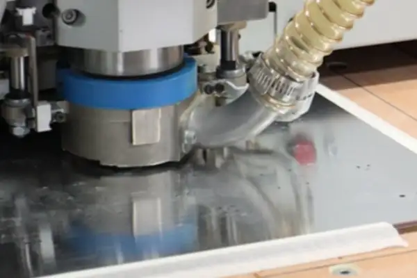
In multilayer PCB production, substrate stability is often the key to achieving
- 중소규모 배치 생산 전문가
- 고정밀 PCB 제작 및 자동화된 조립
- OEM/ODM 전자 프로젝트를 위한 신뢰할 수 있는 파트너
영업 시간: (월~토) 9:00~18:30