
Heat Dissipation Challenges and Solutions in PCB Circuit Board Design
Circuit boards are more than just that green board in a phone
I recently discovered an interesting phenomenon while researching high-frequency circuit design: many people overemphasize the number of PCB layers and wiring density while ignoring something more fundamental—the impact of material properties on signal quality.
Last year, while debugging a millimeter-wave module, I encountered a frustrating problem: despite following textbook impedance matching, signal distortion persisted. It wasn’t until I replaced the standard FR4 material with a low-dk PTFE vinyl ester substrate that I realized—the dielectric constant of the dielectric material directly affects signal propagation speed.
This reminds me of a mistake I made early in my RF circuit design: choosing a standard epoxy resin substrate to save costs resulted in severe losses in the 5GHz band. At the time, I thought it was a layout issue and made three or four revisions before discovering that the dielectric material’s high Df value was causing energy loss.
The choice of metal substrate is often underestimated. During a test of the heat dissipation performance of aluminum and copper substrates, I found that although copper has a higher thermal conductivity, aluminum actually offers better cost-effectiveness in practical applications, especially for LED driver circuits requiring large-area heat dissipation.
Now, seeing some designs still using traditional FR4 material for high-speed signals makes me want to remind everyone: when signal rates exceed 25Gbps, dielectric loss becomes the primary concern, and special resins or ceramic fillers must be considered.
A common misconception is that thicker laminates are more stable. In fact, increased thickness leads to more pronounced fluctuations in the Dk value, especially in high-frequency environments. In a satellite communication project I handled, the phase consistency of the entire batch of circuit boards failed to meet standards because the substrate thickness tolerance exceeded the limit.
Recently, while experimenting with flexible circuits, I discovered an interesting phenomenon: the same circuit printed on different metal substrates exhibits significantly different transmission characteristics, especially when dealing with high-frequency signals. Stainless steel substrates, despite their lower thermal conductivity, are more stable than aluminum substrates.
These experiences have made me increasingly aware that choosing PCB materials is like preparing traditional Chinese medicine; it requires balancing various parameters. Sometimes, sacrificing a little thermal conductivity for a more stable Dk value is a wiser choice, especially for phase-sensitive applications.
I’ve always felt that the most fascinating aspect of PCB manufacturing is that it’s actually an art process full of variables. Many people think that they can perfectly reproduce a circuit board by following the design drawings—this idea is too naive.
I remember being taught a lesson by reality the first time I tried to make a double-sided board myself. My meticulously designed circuit diagrams were completely distorted when translated into actual PCB boards: the fine traces became blurred during etching; vias that should have been precisely aligned shifted slightly due to substrate thermal expansion; even the simplest drilling step resulted in burrs in several critical areas due to drill wear.
These experiences taught me a valuable lesson: even the most advanced design software cannot simulate the subtle variations in the production environment.
Take etching, for example: changes in workshop temperature and humidity affect the activity of the etching solution; differences in copper foil thickness lead to varying degrees of edge etching; even different batches from different substrate suppliers can produce visually noticeable differences in the final result.
During a factory visit, I noticed an interesting phenomenon: experienced workers would use a flashlight shining at an angle to check the reflection on the board surface to judge the etching uniformity—this intuitive judgment based on experience is more sensitive than instrument testing.
Now, my understanding of PCB 제조 is completely different: it’s more like a dialogue between the designer and the materials than a one-way instruction. Every time I adjust drilling parameters or try a new developer mix, I can feel the feedback from the materials—this dynamic balance is the essence of manufacturing.
Recently, when we tried replacing traditional substrates with prepregs, we found that although material costs increased by 15%, edge chipping during drilling decreased by 40%, which actually improved the overall yield—sometimes breakthroughs are hidden in these seemingly insignificant details.
A truly good PCB isn’t designed, it’s tuned: you have to understand the quirks of each step to bring the final product close to ideal.
I’ve always felt that people who talk about PCBs often focus on the wrong things. They always emphasize how many layers there are and how advanced the materials are—which is certainly true—but what truly fascinates me is how these little green boards are quietly changing the way we interact with technology.
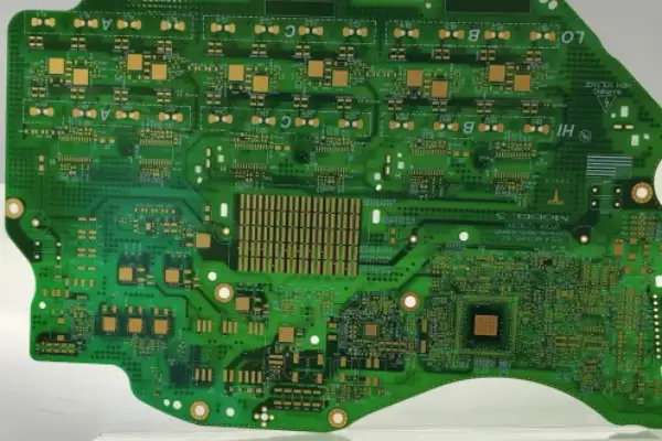
I remember last year when I disassembled an old radio and found a pitifully simple circuit board. It only had single-sided wiring and a few resistors and capacitors to form its entire function. Now, opening the case of the workstation on my desk, used to train neural networks, reveals a completely different world: a densely packed twenty-layer PCB filled with tiny vias and high-frequency signal lines.
Many people think AI is just a bunch of code running in the cloud, but in reality, every intelligent decision must be implemented through physical hardware. Even the most powerful algorithms will get stuck at signal transmission bottlenecks without a well-designed PCB. I’ve seen teams spend months optimizing models only to lose 30% of performance due to improper PCB layout.
The manufacturing process is often overlooked. I was surprised to see a small PCB factory still manually inspecting for defects, while a modern factory was automatically detecting micron-level errors using machine vision. This shift isn’t just a technological upgrade; it’s an evolution in mindset.
Some designers now rely too heavily on AI-assisted tools, which can quickly generate layouts, but lack an understanding of the actual flow of current. I prefer to first sketch the overall structure by hand and then refine the details with software—this laborious approach avoids many later problems.
Environmental protection is often reduced to marketing slogans in the PCB industry, but I’m more concerned with actual results. I once tested a recyclable substrate, and its performance degraded significantly at high frequencies. True sustainable manufacturing should extend product lifespan, not simply pursue biodegradable materials.
Ultimately, the PCB is like the skeleton of technology; it doesn’t directly think, yet it supports all intelligent activities. Every time I see those copper wires winding and stretching across the insulation layer, I think this is probably the most realistic physical expression of the digital world.
I’ve recently noticed that many people’s understanding of PCBs is still limited to the “green substrate” of a circuit board. In reality, a good PCB design is far more complex than simply drawing circuits.
Last year, while helping a friend redesign an audio device, I discovered an interesting phenomenon: they spent a lot of money on high-end components but neglected the most basic aspect—the choice of PCB material. As a result, the device consistently produced noise at high frequencies, and after repeated troubleshooting, it was discovered that the substrate material’s dielectric constant was unstable at high frequencies. These kinds of details are often more important than pursuing a particular parameter.
That green protective coating on the PCB is quite interesting. We usually call it the solder mask, but its function goes far beyond simply preventing soldering. A test once revealed that the appropriate solder mask thickness can even fine-tune signal integrity, although this requires proper impedance design.
Regarding circuit precision, the industry is always competing to see who can make the finest lines, but I think blindly pursuing micron-level line widths can easily lead to problems. I’ve seen too many cases where excessively close line spacing caused a sharp drop in yield during mass production. Sometimes, appropriately relaxing requirements and using more mature processes can actually result in higher overall reliability.
The curing process is often overlooked. A factory skipped the complete curing process to shorten production time, resulting in products developing delamination and blistering issues after three months of use. Thermal management is a hidden hurdle in PCB design; poor handling renders even the best circuit design useless.
Regarding surface treatments, immersion gold does provide a smoother surface, but beyond cost considerations, the specific application scenario must be taken into account. For example, in industrial environments, simple tin plating might be more durable; in certain high-humidity environments, I’ve even recommended special anti-oxidation treatments.
Controlling the temperature profile during multilayer board lamination is a technical skill. I remember visiting a factory where they successfully solved the inner layer misalignment problem by adjusting the heating rate. This kind of empirical data is often more practical than theoretical formulas.
The testing phase is the easiest to cut costs in, yet it’s precisely the part that shouldn’t be skimped on. Flying probe testing can find obvious open and short circuits, but for hidden defects, functional testing is still necessary. The smartest approach I’ve seen is to reserve test points during the design phase, which is far more efficient than retrofitting later.
Many engineers now rely excessively on simulation software. However, PCB design needs to incorporate practical experience. For example, allowing adjustment space for high-frequency signals during routing is more reliable than relying solely on simulation results. After all, the variables in actual production far outnumber those set in software.
I’ve seen many people overcomplicate PCB design—as if you need to master a bunch of technical jargon to even get started. But in my experience, those densely packed lines hide many interesting nuances.
Take component layout, for example! Once, I helped a friend modify the design of a small device—he had crammed all the components together to save space; but when soldering, the soldering iron couldn’t even reach! Later, we moved a few large capacitors to a corner; the whole board suddenly looked much better, and even later debugging was much easier.
Speaking of soldering, solderability is a huge issue! I remember when I first started working with PCBs, I used a batch of cheap boards; the surface treatment was sloppy, resulting in constantly loose solder joints. After much troubleshooting, I finally discovered it was copper oxidation! Now, I pay special attention to the surface finish when choosing boards; after all, nobody wants to rework something over something so small, right?
Another small detail that might be easily overlooked—the clarity of the silkscreen layer is really important! Last week I dug out some PCBs I made a few years ago; the markings were almost worn away. Now, even changing a component requires spending ages referring to the circuit diagram! So now I’d rather spend a little more money to make the silkscreen clearer, especially those easily confused polarity markings.
Actually, the more you do PCB design, the more you realize it’s like tidying up a room—you don’t necessarily need the latest tools; you just need to ensure every component has its proper place and the circuitry is clear and organized. This will prevent headaches during later maintenance!
I’ve always felt that the most fascinating aspect of PCB design isn’t the complex circuitry, but rather the handling of seemingly insignificant details. Take that green protective coating, for example. Many people think it’s just for aesthetics, but this solder mask layer actually improves the reliability of the entire PCB by several levels.
I remember once debugging a high-frequency board and finding that the signal was inexplicably attenuating. Later, I discovered that uneven solder mask thickness was causing impedance variations. This experience made me realize that even the most basic protective coating has a significant impact on the overall performance of the PCB.
When designing, I pay special attention to the handling of tiny vias, especially buried vias in multilayer boards. Although completely invisible from the outside, they act like secret channels within the circuit board, ensuring smooth signal transmission without taking up valuable surface space. However, this design does increase manufacturing difficulty; sometimes, several versions of the design need to be revised to determine the path of a few key signals.
I particularly enjoy observing the texture of boards from different manufacturers. Some manufacturers have exceptionally glossy solder mask layers, like a well-fitting raincoat for the entire PCB board; while others appear simpler, yet offer more robust protection. These subtle differences often reveal the manufacturer’s technical expertise.
Recently, I was experimenting with a six-layer board and discovered that proper silkscreen markings on the surface can greatly simplify subsequent assembly processes. Although these white characters have no impact on circuit performance, they are indispensable markers in the production process. Once, I was lazy and forgot to add component markings, resulting in the assembly worker soldering the chips backwards—a lesson I still remember vividly.
In fact, behind every successful PCB lies countless such meticulous considerations. The meticulously arranged conductive channels, the perfectly applied protective coating, and the clear assembly markings—these elements combine to create a sophisticated work of industrial art. Sometimes, examining the textures on the circuit board under light, I feel it possesses a vitality more profound than any painting.
The longer I work in this field, the more I understand that good design is never about pursuing the ultimate in a single metric, but about finding the most elegant balance within various constraints. Like a musician composing a piece, we are essentially creating our own electronic symphony using copper foil and substrate.
Every time I see my designed board successfully light up, I can’t help but smile. This sense of accomplishment is probably the greatest motivation that sustains our continuous refinement of every detail.
Every time I disassemble an old phone and see those delicate little green boards inside, I always think—these seemingly insignificant PCBs are the true skeleton supporting the operation of modern technology. Many people think that circuit boards are merely carriers for connecting components, but I’ve always believed they are more like the nervous system of electronic products, transmitting every instruction for the device’s operation.
Having worked on numerous printed circuit board (PCB) design projects, I’ve found that the true determinant of performance isn’t the most cutting-edge technology, but rather the solidity of the fundamental design. Once, when our team was designing a PCB for high-frequency signal processing, we initially blindly pursued the latest materials, resulting in severe signal interference. Later, switching to a mature substrate with a reasonable routing scheme led to significantly improved stability. This made me realize that innovation doesn’t necessarily mean overturning everything. For example, in RF circuit design, the integrity of the ground plane and the placement of power supply decoupling capacitors are often more important than the dielectric constant of the dielectric material. Proper via design and signal return path planning can significantly reduce crosstalk, while blindly using high-frequency dedicated substrates while neglecting basic layout can lead to impedance mismatch and signal reflection.
Currently, the industry is always discussing how fine and dense the circuitry should be, as if nanometer-level precision is the ultimate goal. However, many applications don’t require such extreme precision. Overly pursuing parameters can sacrifice reliability and cost-effectiveness. For example, some industrial control equipment can operate stably for over a decade using conventional multilayer circuit boards; why force a high-density solution? Taking the signal control system of rail transit as an example, its PCB typically uses a 4-8 layer structure with a line width and spacing of 6-8 mil. While this design doesn’t pursue extreme miniaturization, it ensures long-term stability under vibration and high-temperature environments by increasing copper thickness and surface treatment processes. Conversely, some consumer electronics products, in pursuit of thinness and lightness, compress line widths to below 3 mil. Although this achieves high-density integration, it also leads to decreased yield rates and heat dissipation problems.
The widespread adoption of flexible circuit boards has indeed brought more design possibilities, but rigid-flex boards often face challenges in interface reliability in practical applications. I’ve seen too many failures caused by improper design of bending areas, so now when designing solutions, I pay more attention to structural adaptability rather than simply emphasizing flexibility. For example, in wearable devices, the bending area connecting flexible circuits to a rigid motherboard requires precise calculation of the radius of curvature to avoid stress concentration. At the same time, the material and thickness of the cover film affect flexibility and bending resistance. Although polyimide substrates have good flexibility, without proper reinforcing ribs, conductor breakage is prone to occur at frequent bending points.
Speaking of future trends, I believe the most crucial breakthrough for the PCB industry isn’t in technical parameters but in a shift in design thinking. For example, how to achieve better heat dissipation under standard processes or how to reduce electromagnetic interference through layout optimization. These seemingly simple improvements often enhance the user experience more than chasing cutting-edge specifications. For instance, optimizing component layout, placing high-heat-generating chips near the board edge, and adding thermal via arrays, can achieve excellent heat dissipation even with a standard FR-4 substrate. Regarding electromagnetic compatibility, adopting the “3W rule” for high-speed signal lines—maintaining a spacing of three times the line width—effectively suppresses crosstalk. Implementing this fundamental design principle is more practical than simply pursuing high-frequency materials.
Recently, while helping a friend modify an old radio, I discovered that although current PCB manufacturing processes far surpass those of the past, the simple and efficient wiring approach is still worth learning. Sometimes, the most effective solutions lie hidden in these fundamental designs. Old-fashioned radios used single-sided PCBs with large-area grounding and modular partitioning. While simple in manufacturing, this resulted in clear signal paths and strong anti-interference capabilities. This design philosophy remains applicable to modern IoT devices. For example, in sensor node board layouts, analog and digital circuits are strictly separated, and a star grounding method is used to significantly reduce noise interference.
I’ve always found printed circuit boards (PCBs) quite interesting. Many people might think it’s just a green plastic sheet covered in copper wires. But if you’ve ever disassembled an old radio or mobile phone, you’ll find that those intricate lines actually hide a lot of intricacies.
I remember my first encounter with PCBs was in a university lab project. We were using basic single-sided boards and had to etch the circuits ourselves; a slight mistake could corrode and break the tiny traces. That’s when I truly understood why my professors always said designing a circuit is one thing, but turning that circuit into a usable printed circuit board is entirely another.
Looking back on those experiences now, they’ve given me a different perspective on electronic products. For instance, many people only focus on processor parameters when changing phones, unaware that the real determinant of stability is often the multi-layered PCB on the motherboard. It requires arranging over a dozen layers of circuitry within a space the size of a fingernail while ensuring high-frequency signals don’t interfere with each other—this is far more difficult than simply stacking hardware specifications.
I’ve seen many DIY enthusiasts spend a fortune on top-of-the-line components, only to have their overall performance compromised due to the use of cheap printed circuit boards. It’s like using a race car engine with bicycle tires—not that the materials are bad, but the components simply don’t work together effectively.
Sometimes, browsing electronics forums, you see people debating which substrate is better for high-frequency circuits. These discussions often overlook a more fundamental issue—good design is always based on trade-offs made for specific application scenarios. Just as you can’t use the same PCB to simultaneously meet the needs of military equipment and smart bracelets, their reliability standards and space constraints are completely different.
Last year, while repairing a friend’s drone, I disassembled its flight control module and saw the complex eight-layer structure. It suddenly dawned on me that the evolution of modern electronics to its current form is not simply a matter of miniaturizing components. Those seemingly ordinary brown boards actually house a complete ecosystem, from power management to signal transmission.
Now, whenever I see a new electronic product released, I pay more attention to its internal layout. Are the heat dissipation holes positioned to avoid critical circuits? These details often reflect the design team’s dedication more than benchmark scores. After all, the moment the chip is soldered onto the printed circuit board is the true beginning of technology implementation.
I’ve always felt that the most fascinating aspect of PCB design lies in the possibilities it brings to electronic products. Remember the green circuit board you saw when you first disassembled an old radio? Those neat lines resembled a city road map. Now, the PCB boards we face have evolved to the point where they can be bent and folded like paper.
Last week, I was particularly struck by this while helping a friend repair a smart bracelet. That flexible substrate, smaller than a fingernail, was covered with lines thinner than a human hair. The biggest advantage of this flexible PCB isn’t the technical parameter of how many times it can be bent, but rather that it truly changes the product’s form factor. You see, the seamless wristband design of today’s bracelets is thanks to this technology.
Regarding the choice of substrate material, I have a different opinion. Many people blindly pursue the latest materials, but ordinary FR-4 substrates are sufficient for most household appliances. Last year, when I assembled my own speakers, I used ordinary fiberglass substrates, and the sound quality wasn’t affected at all; in fact, I saved 30% on costs.
Recently, while researching drone flight control systems, I found rigid-flex PCBs particularly interesting. The motherboard needs to be rigidly fixed, while the part connecting to the camera needs to rotate constantly—this is where the rigid-flex design comes in handy. However, this type of PCB board has very high requirements for soldering processes; even a slight mistake can lead to broken circuits.
I’ve noticed that many engineers tend to get bogged down in technical details, such as obsessing over the exact micrometers of the line width. But in practical applications, the overall layout is more important. I once saw a power module where the high-voltage lines and signal lines were placed too close together, causing interference. This kind of fundamental error is more fatal than failing to meet technical specifications.
Many smart home devices now use metal substrates, which do offer better heat dissipation, but the cost is also higher. I think it depends on the specific application scenario. Devices like routers that are constantly on are worth investing in, while appliances used only occasionally don’t need to pursue extreme heat dissipation.
Recently, while trying to transform an old mobile phone into a smart home hub, I was amazed by the incredible precision of current IC substrates. Looking at those circuits under a microscope is like examining a miniature work of art. However, the price of this precision is that repair is virtually impossible; once damaged, the entire board must be replaced.
In fact, the most important thing in PCB design is spatial imagination—the ability to foresee the three-dimensional assembly effect on a two-dimensional drawing. Once, a board I designed couldn’t be fitted into its casing because I hadn’t considered the component height. This practical experience is more profound than any textbook.
Every time I see my PCB design become a usable product, I feel a special sense of accomplishment. Perhaps this is why I still enjoy drawing circuit diagrams by hand, even though there are many automated routing tools available now. This creative process from scratch is the most captivating part.
Every time I see those complex circuit designs, I think about the space game behind them. We always want to cram more functionality into a limited space, and the emergence of multilayer boards has perfectly solved this dilemma. I remember the first time I disassembled an old radio, the thin PCB inside… The components on the board were pitifully sparse, while nowadays even a casual smartphone motherboard is as intricate as a mille-feuille cake.
Many people fall into the misconception that the more advanced the material, the better. In reality, the key is the application scenario. I’ve seen people use high-frequency specialized boards for ordinary household appliances, which is a complete waste of resources—like putting racing tires on a scooter. There’s no need. FR4, a conventional material, is reliable enough in most cases. Only in military or aerospace applications do we need to consider more specialized substrates.
What I find truly interesting is the trade-offs in the design process. Adding multiple layers can indeed improve performance, but cost and heat dissipation issues also arise. Once… In a project I participated in, the pursuit of thinness and lightness resulted in compressing an eight-layer PCB to six layers, causing a 20% drop in yield during mass production. Sometimes, excessively pursuing technical specifications can deviate from actual needs.
Many engineers today like to blindly stack layers, ignoring the elegance of simple design. Some classic circuits can operate stably for over a decade using double-sided boards, while those massive twenty-layer boards might collapse entirely due to a single via failure. After working in this field for a while, you’ll find that the best designs are often found at a balance point under constraints, not simply by piling on components.
Every time I take apart an old phone and see that green board inside, I think of it as a miniature city. The densely packed lines are like streets, integrated circuits are like skyscrapers, and the tiny resistors and capacitors are like convenience stores on the street. Many people think of a PCB as just a carrier, but I prefer to see it as the skeleton of an electronic product—without a skeleton, even the smartest brain can’t stand up.
I remember the first time I soldered a circuit board myself, I set the soldering iron temperature too high, and the copper foil curled up. This lesson taught me that even the most perfectly designed circuit is useless if the board material or manufacturing process is inadequate. Some manufacturers cut corners on base materials to reduce costs, causing equipment to malfunction quickly – a particularly short-sighted approach.
My recent experience repairing a drone made me realize the importance of the fine, hair-like wiring on flight control boards. A single break in one area can paralyze the entire system. It’s similar to a city’s power grid: a small fault on a main road can trigger a chain reaction. Therefore, when designing circuits, I always include extra redundant lines, like building backup roads for a city.
Some people are always chasing the latest and most innovative chips, neglecting the fact that the circuit boards supporting them require even more craftsmanship. I’ve seen mobile phone motherboards bulge after only six months of use, and industrial controllers that have worked stably for ten years – the difference lies entirely in the materials and manufacturing process of the PCB. A good circuit board should be like the load-bearing walls of an old house, silently supporting it for decades without deformation.
Recently, I tried using flexible materials to make circuits for wearable devices and discovered a completely different world. Traditional rigid PCBs don’t work here; the circuitry needs to be like the weave of textiles, both conductive and flexible. This exploration made me realize that the form of the circuit board can, in turn, define the possibilities of the product.
Ultimately, while the soul of an electronic product lies in its chip, its physical body is always this unassuming PCB. It must withstand the high temperatures of soldering, resist the wear and tear of daily use, and ensure the accuracy of signal transmission. Next time you marvel at the powerful functions of a device, perhaps you should also consider the physical foundation that supports those functions.
Recently, while tidying up my studio, I found several PCBs from ten years ago. Looking at the yellowed substrate and the oxidized, darkened traces, I suddenly felt a pang of emotion—this thing is truly the most silent workhorse in the world of electronics.
Many people think a PCB is just a layer of solder mask and a few lines. Actually, the choice of substrate alone is enough to cause headaches. Once, while helping a friend modify an RF module, I discovered that ordinary FR4 material was practically a signal black hole at high frequencies. It was only after switching to Teflon substrate that the problem was solved. That feeling is like changing the cables in a speaker—both are copper conductors, but the purity is different, resulting in vastly different sound clarity.
The unit of measurement for copper thickness, ounces, is quite interesting. Once, while making a motor drive board, I was lazy and used standard 1-ounce copper. As a result, the circuitry got so hot under full load that it could fry an egg. Later, the thickness was changed to 3 ounces, which increased the cost, but the temperature control was significantly improved. Now, when I see high-power designs, I always glance at the copper thickness parameter; after all, safety redundancy is far more important than saving a few dollars.
What truly changed my perspective on PCBs was repairing an old radio. Upon disassembling it, I discovered that the 50-year-old board, using a paper substrate, was still functioning perfectly. While modern fiberglass boards offer superior performance, they’ve lost that vintage resilience. Sometimes, high performance doesn’t equate to good design; the difference between solid wood furniture and composite boards isn’t hardness, but rather appropriate elasticity.
Recently, I tried using an aluminum substrate for LED light strip heat dissipation, and the effect was indeed amazing, but I’m always worried about the metal layers breaking when bending them. This kind of dilemma is probably the daily reality for engineers—finding a balance between mechanical strength and electrical performance. Designing a PCB is like building with blocks, except our blocks conduct electricity, generate heat, and have to withstand extreme environments for years.
Perhaps this is the most fascinating aspect of PCBs; they’re never the main character, but without them, all electronic devices would become a pile of disassembled parts.
Whenever I see the intricate internal structures of electronic devices, I’m always reminded of those unassuming yet crucial PCB circuit boards. I remember the awe I felt when I first disassembled an old radio and was struck by the dense wiring—these seemingly simple copper traces actually carried the soul of the entire device.
Performance in high-frequency applications often best reveals the true capabilities of a PCB. I’ve seen many projects suffer severe signal attenuation due to unsuitable substrate selection. Sometimes, a seemingly minor design flaw can drastically reduce the performance of the entire communication system.
Currently, many engineers prioritize feature stacking during the design phase, neglecting the most basic signal integrity considerations. Take, for example, a device we recently tested; despite its fancy features, it suffered from significant signal crosstalk in high-frequency environments. This made me realize that even the most complex functions need to be built upon a solid foundation of design.
Different applications place vastly different demands on PCBs. For instance, the reliability requirements of medical equipment and industrial control far exceed those of consumer electronics. I’ve encountered design specifications for industrial-grade equipment, which have almost stringent requirements for material selection and manufacturing standards. This has given me a profound understanding of why some products can operate stably for over a decade, while others fail after a short period. When choosing a PCB supplier, I prioritize whether their engineering team truly understands the product requirements rather than simply comparing prices. Too many cases have shown that cost savings in the early stages often come back to bite during later debugging and maintenance. A good design team considers often overlooked details like thermal management and electromagnetic compatibility from a holistic product perspective.
With technological advancements, more and more devices are adopting hybrid material solutions to balance performance and cost. This brings more design possibilities but also increases complexity. I believe that truly excellent engineers in the future will be those who can find the optimal balance under multiple constraints, rather than simply pursuing the ultimate performance of a single metric.
Circuit boards are more than just that green board in a phone
From disassembling old routers to visiting electronics manufacturing plants, I gradually realized
As an electronics enthusiast, I’ve come to understand firsthand the impact of
- 중소규모 배치 생산 전문가
- 고정밀 PCB 제작 및 자동화된 조립
- OEM/ODM 전자 프로젝트를 위한 신뢰할 수 있는 파트너
영업 시간: (월~토) 9:00~18:30