
Heat Dissipation Challenges and Solutions in PCB Circuit Board Design
Circuit boards are more than just that green board in a phone
Recently, while chatting with some friends who do power supply design, I discovered an interesting phenomenon—everyone is quite experienced in choosing ordinary circuit boards, but they become hesitant when it comes to high-voltage environments. Actually, it’s not that mysterious; the key is to understand that the rules of the game change when the voltage increases.
I’ve seen many engineers directly apply conventional PCB design concepts to high-voltage projects, resulting in either a pitifully short product lifespan or products emitting smoke during testing. Ultimately, ordinary circuit boards and high-voltage circuit boards are completely different things, like the difference between a family sedan and an SUV—both have four wheels, but their handling of complex road conditions is worlds apart.
I remember a medical equipment project I participated in last year. The client initially chose an ordinary PCB supplier to save money, resulting in creepage during high-voltage testing. The problem was only solved by finding a professional high-voltage PCB manufacturer. This lesson tells us that when the operating voltage exceeds a certain threshold, the insulation performance of the material becomes a matter of life and death.
Interestingly, many people think that high-voltage circuit boards are simply about thickening the copper layer. The real challenge lies in controlling the conductor spacing and dielectric thickness. I once visited a high-voltage PCB supplier’s lab and saw them using special processes to treat the surface of the boards with such precision that it was like micro-sculpture.
Currently, some manufacturers on the market use the high-voltage label but are actually just making changes to ordinary circuit boards. A truly reliable high-voltage PCB manufacturer will discuss in detail the environmental parameters of your application scenario, such as humidity changes and temperature cycling, all of which affect the final performance. After all, in a high-voltage environment, any oversight can lead to disaster.
The professional manufacturers I admire most will recommend different grades of boards based on your actual needs, rather than simply pushing the most expensive products. Not all high-voltage applications require military-grade configurations; sometimes over-design can increase unnecessary costs.
Speaking of future trends, I think flexible high-voltage circuit boards are an interesting direction. With the development of new energy vehicles and wearable devices, the demand for circuit boards that can withstand high voltage and adapt to complex shapes will increase significantly. However, this field has higher requirements for materials and processes, and currently there are not many manufacturers capable of doing it.
Ultimately, choosing a high-voltage PCB is like finding a partner. Technical strength is important, but whether the other party is willing to take the time to understand your specific needs is key. A good supplier will become your technical support, not just a simple buyer-seller relationship.
I recently chatted with a friend who works in power supply equipment, and he mentioned choosing a high-voltage PCB supplier, which reminded me of the pitfalls I’ve encountered. Many people think that any PCB factory can make high-voltage circuit boards—this idea is too dangerous. Last year, our team stumbled on a medical imaging device due to a design flaw in the high-voltage section. To save on budget, we chose a regular PCB manufacturer, but during prototype testing, the insulation layer was directly breached, nearly delaying the entire project. We only resolved the issue by switching to a professional high-voltage PCB manufacturer; their materials and processes were completely different.
The difference between a regular PCB and a high-voltage PCB is like the difference between a bicycle and an off-road vehicle. The former might perform well on flat roads but fail on complex terrain, while a professional high-voltage PCB supplier controls everything from material properties—such as the substrate’s arc resistance and copper foil adhesion—these details are crucial to the device’s stability.
During a visit to a high-voltage PCB manufacturer’s workshop, I noticed their testing process involved three or four more steps than a regular factory, especially their partial discharge testing equipment, which can simulate extreme voltage fluctuations. This level of investment is something small factories are unlikely to undertake.
Many industries are now upgrading their high-voltage equipment, such as charging piles for new energy vehicles and industrial laser equipment. These fields have increasingly higher voltage withstand requirements for PCBs. If we continue to choose suppliers using the old approach, we may end up incurring significant costs to rectify the situation later.
I believe the most practical way to choose a high-voltage circuit board supplier is to see if they dare to present their test data, such as withstand voltage values, aging curves, temperature cycling test reports, and other hard indicators. These are far more effective than any number of case studies touted by salespeople.
Recently, I’ve noticed that many people’s understanding of high-voltage circuit boards is still at a basic level. In reality, these products are far more complex than imagined. I remember last year when our lab needed to customize a special high-voltage PCB, we discovered that there were very few truly reliable high-voltage PCB manufacturers on the market.
That experience taught me a valuable lesson: choosing the right substrate material is paramount. Some suppliers recommend ordinary FR4 material to reduce costs, but using it in a high-voltage environment is a recipe for disaster. Especially when the operating voltage exceeds a certain threshold, the material’s insulation performance becomes the decisive factor.
I particularly admire manufacturers who insist on using PTFE material. Although it’s more difficult to process, its performance is undeniably stable. Once, I visited a high-voltage PCB supplier’s workshop and saw how they used special processes to handle PTFE substrates—the entire process resembled the assembly of precision instruments.
Many people fall into the trap of thinking that simply increasing spacing is enough when it comes to insulation design. In reality, there are many more factors to consider, such as material composition and pollution levels—details that are often overlooked.
A high-voltage circuit board manufacturer I worked with left a deep impression on me. They intervened during the design phase, helping clients analyze potential risks in real-world application scenarios. This service-oriented approach is rare in the industry.
Ultimately, safety in high-voltage environments allows for no carelessness. When choosing a partner, you can’t just look at the price; you must consider their ability to control details—that’s where the investment is most worthwhile.
Having worked in the high-voltage circuit board industry for several years, my deepest realization is that many people think that simply increasing the spacing is enough, but that’s not the case at all. True high-voltage design is more like battling an invisible electric field; you have to anticipate its trajectory.
I remember once when we were designing a high-voltage PCB, we only focused on the spacing parameters. During prototype testing, corona discharge appeared near a seemingly insignificant right-angle trace. Later, using simulation software, we discovered that the electric field strength at that sharp corner was more than three times higher than the average area. This experience made me realize that the electric field distribution under high voltage is not uniform at all; it tends to concentrate in gaps and sharp corners, like water flowing through them.
Choosing a reliable high-voltage PCB manufacturer is crucial. Once, a new supplier provided boards with unstable dielectric constants, causing significant fluctuations in insulation performance across the entire batch at different temperatures. A good high-voltage PCB supplier will repeatedly confirm the application scenario with you—is it continuous high voltage or pulsed high voltage? What is the ambient humidity? These details directly affect material selection, such as high-voltage circuit boards operating in humid environments for extended periods.
Multilayer board design is even more interesting. Once, we tried placing high-voltage lines with different potentials on adjacent layers, although this met safety spacing requirements.
Speaking of surface treatment:
My current habit is to perform 3D electric field simulations for every high-voltage design.
A recent project gave me a new understanding of “distance.” The client required 5kV isolation on a compact medical device PCB, which conventional creepage distances simply couldn’t accommodate.
Ultimately, the biggest pitfall in high-voltage design is relying on past experience.
I recently chatted with a friend who works in medical device R&D, and he mentioned encountering many pitfalls when choosing a high-voltage circuit board supplier. Some manufacturers offered extremely low prices and fast delivery times, but once the samples arrived, they couldn’t pass the withstand voltage test at all. This reminded me that high-voltage applications really can’t be handled by just finding any manufacturer that can make ordinary circuit boards.
Many people might think that high-voltage circuit boards are simply about wider line spacing and better insulation. Actually, there’s a lot more to it than that. For example, choosing insulation materials isn’t just a matter of looking at a parameter table; you have to consider the aging characteristics of the materials under long-term high electric fields. I’ve seen some products that passed initial tests, but after a few months of operation, their insulation resistance started to drop significantly.
When looking for a high-voltage PCB manufacturer, what I value most is their testing process. Ordinary circuit boards might only require random sampling, but high-voltage boards must undergo comprehensive testing on every single one. Especially the withstand voltage test; it can’t just be a simple matter of passing a high voltage through to see if it sparks, but it needs to simulate the actual working environment, including the impact of temperature and humidity changes on insulation performance. Some manufacturers skip these steps, but this is often the beginning of hidden problems.
Certification is also a major issue. A reputable high-voltage PCB supplier should provide a complete material certification chain, with corresponding safety certificates for everything from the substrate to the solder resist ink. I once encountered a manufacturer that claimed their boards were UL certified, but when asked to produce specific model certification documents, they started making excuses. These kinds of details often reveal a manufacturer’s level of professionalism.
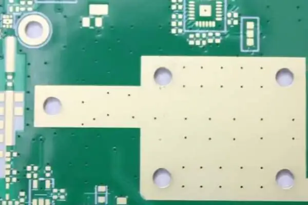
Many high-voltage applications now require miniaturized, high-density designs, which places higher demands on manufacturing processes. For example, the interlayer alignment accuracy of multilayer high-voltage circuit boards must be controlled within an extremely small error range; the treatment of the hole walls after drilling must be particularly meticulous, as any burrs can become discharge points. These process details often determine the final reliability of the product.
I think choosing a high-voltage PCB is like buying insurance; the differences may not be apparent in normal times, but their importance becomes clear when problems arise. Rather than spending a lot of money on rectification later, it’s better to find a truly professional partner from the start. After all, when it comes to safety, you can never be too cautious.
Sometimes, investing more in the initial selection and testing can save a lot of trouble later. This principle applies to many industries, but it is especially evident in the high-voltage field because small oversights can lead to major problems.
I’ve always found the work of high-voltage PCB manufacturers quite interesting. Many people think it’s simply a matter of widening the trace spacing on a regular PCB, but that’s not the case at all. Once, I encountered a project where a client brought us a design for a regular PCB, wanting to directly convert it to a high-voltage version. Upon reviewing the drawings, we realized it was completely impractical—the voltage alone could break down even the air. For example, in 10kV applications, even increasing the conductor spacing to 5mm, without considering the dielectric constant and surface coating characteristics of the substrate, electric field concentration can still lead to surface discharge. In such cases, specialized high-dielectric-strength substrates, such as PTFE or ceramic-filled epoxy resin, must be used to effectively suppress breakdown.
Finding a reliable high-voltage PCB manufacturer is crucial. I’ve seen too many examples of entire batches of products being scrapped due to choosing the wrong supplier. One medical equipment client, trying to save money, had a small workshop make high-voltage PCB samples that looked okay during testing, but encountered various breakdown problems during mass production. They later contacted us, only to discover that the substrate’s insulation performance was substandard. In practice, reputable manufacturers employ vacuum lamination processes to ensure the dielectric layer is bubble-free and monitor the glass transition temperature using thermal analyzers to prevent insulation performance degradation at high temperatures. These process details often require expensive testing equipment, but they are fundamental to ensuring long-term reliability.
Many details must be considered during the design phase. For example, creepage distance cannot be considered only in a two-dimensional plane but also in three-dimensional space. Once, we helped a power supply manufacturer redesign their original solution, which was prone to problems in humid environments because it didn’t consider the impact of surface contamination on insulation under condensation conditions. We added slotted grooves and barrier dam designs, extending the surface creepage distance three times compared to the straight-line distance. We also specified the use of a CTI600-rated anti-leakage substrate, which maintains its surface resistivity even in humid environments.
The biggest threat to high-voltage PCBs is partial discharge, a problem that is often insidious and may only become apparent after six months of use. We now incorporate protective structures into our designs, like putting a protective suit on the circuit. While this increases costs slightly, the reliability improvement is significant. For example, installing ring-shaped grounding rings at the edges of high-voltage conductors and using corner designs with gradually varying curvature to avoid electric field concentration can increase the partial discharge initiation voltage by more than 30%. Recently, we’ve also started using ultraviolet fluorescent dye injection detection, which can detect micro-discharge phenomena invisible to the naked eye at the prototype stage.
When choosing a high-voltage PCB supplier, my most important factor is their testing capabilities. Certification alone isn’t enough; I need to see how they actually conduct withstand voltage tests. Good manufacturers simulate various extreme environments, not just standard tests at room temperature and pressure. Truly professional laboratories conduct dielectric strength tests after temperature cycling, such as requiring a withstand voltage test of 2.5 times the operating voltage after 100 cycles within a range of -40℃ to 125℃. Some high-end applications also require partial discharge quantity testing, requiring a discharge quantity of less than 5pC to pass acceptance.
Actually, the most satisfying thing about making high-voltage circuit boards is that you learn something new every time you solve a new problem. A project I just completed last week required the client to achieve a 10kV isolation distance in a limited space. We finally solved it using a special sandwich structure. This kind of challenge is much more interesting than simply drawing circuits. We employ alternating layers of ceramic substrate and FR4 material, precisely calculating the dielectric constant distribution of each layer to achieve a gradient attenuation of the electric field strength in the vertical direction. This structural design not only meets safety spacing requirements but also achieves a thickness 40% thinner than traditional solutions.
I believe that future high-voltage PCBs will increasingly emphasize integration—not simply increasing voltage, but rather more compactly combining high-voltage components with low-voltage control circuits. This presents new challenges for both design and manufacturing processes. Some manufacturers are already attempting multi-layer embedded capacitor technology on a single substrate, forming a virtual shielding layer in the high-voltage area through nano-coatings. This technology requires solving the problem of matching thermal expansion coefficients, but once successful, it allows signal acquisition circuits to be directly embedded within the high-voltage module, significantly improving system response speed.
Recently, I chatted with an engineer working on a new energy project and discovered an interesting phenomenon—their team spent six months testing various high-voltage circuit board samples before finalizing their solution. This reminds me of a common misconception when choosing high-voltage PCB suppliers: focusing excessively on the numbers on the technical specifications while neglecting the compatibility with the actual application scenario.
I remember visiting a company specializing in medical equipment last year; their CT scanners need to withstand tens of thousands of volts internally. The engineer pointed to the densely packed circuit boards in the control room and explained that each of these seemingly ordinary high-voltage circuit boards had undergone special treatment, even taking into account the molecular structure of the substrate. This made me realize that stability under high-voltage conditions cannot be achieved simply by piling on materials. For example, in medical imaging equipment, high-voltage circuit boards need to withstand instantaneous pulse voltages while ensuring that electromagnetic interference does not affect image quality. This requires finding a precise balance between parameters such as dielectric constant and dielectric loss.
Some suppliers like to boast about the number of certifications they have obtained, but what truly matters is whether they understand the operating environment your product will be in. For example, in high-voltage applications, medical equipment requires absolutely no noise, while industrial equipment may prioritize high-temperature resistance. Especially in heavy industrial settings, high-voltage PCBs may need to operate continuously in harsh environments filled with metal dust, where surface insulation resistance and contamination resistance become critical indicators.
The most extreme example I’ve seen is a factory that, to save money, chose ordinary PCBs instead of dedicated high-voltage boards. After three months of operation, carbonization appeared on the circuit boards. They later switched to a professional high-voltage PCB manufacturer, who performed special arc-resistant treatment on the board surface, resolving the issue. This treatment typically includes increasing the thickness of the solder mask layer, using special groove designs to extend creepage distances, and even using ceramic filler materials to improve arc resistance.
Many companies are now focusing on supply chain sustainability, which is particularly important in the high-voltage field. After all, the validation cycle for these products is long, and suddenly changing suppliers could mean re-performing reliability tests that last for months. For example, the automotive industry requires dozens of tests for high-voltage components, including temperature cycling, mechanical vibration, and damp heat aging, a process that can take more than six months.
A friend who manufactures photovoltaic inverters told me that when choosing suppliers, they value their ability to learn from mistakes, as high-voltage circuit board designs often require multiple iterations. Good suppliers proactively offer improvement suggestions rather than simply producing according to blueprints. They will suggest adjustments to the lamination structure or optimization of the grounding design based on the actual application scenario; these detailed improvements often significantly extend product lifespan.
In fact, there’s a very intuitive way to judge the professionalism of a high-voltage PCB manufacturer—see if they can clearly explain the applicable scenarios for different insulation materials. For example, PTFE is suitable for high-frequency applications but has poor mechanical strength, while epoxy resin, although having good voltage resistance, may have thermal expansion issues. Professional engineers will also consider the changes in dielectric strength of materials at different temperatures; for example, the dielectric constant of some materials drops sharply at high temperatures, leading to insulation failure.
Recently, I’ve noticed a trend: more and more companies are starting to require suppliers to provide partial discharge test reports. This is indeed a better reflection of long-term reliability than simple withstand voltage tests, since the biggest fear for high-voltage equipment is the degradation of insulation performance over time. Partial discharge tests can detect tiny air gaps or impurities in the dielectric; these defects will gradually expand under long-term high-voltage operation, eventually leading to breakdown.
Speaking of this, I’m reminded of how some manufacturers, in pursuit of lower costs, choose to reduce copper foil thickness. However, this can be fatal in high-voltage applications. Thin copper foil not only affects current-carrying capacity but also reduces creepage distance. More seriously, under frequent switching conditions, thin copper foil is prone to cracking due to electrothermal stress, leading to localized overheating accidents.
In fact, instead of obsessing over a single parameter, it’s more effective to look at the supplier’s actual case studies. For example, have they produced products at similar voltage levels? Have they handled similar temperature ranges? This practical experience is often more convincing than certificates. Experienced manufacturers will share the problems and solutions they encountered in similar projects; this knowledge transfer is more valuable than standard parameters.
Finally, choosing a high-voltage PCB essentially involves balancing multiple factors. Safety standards should be paramount, but actual cost and production cycle must also be considered. Sometimes, overly conservative designs can lead to wasted resources. For example, while meeting safety clearance requirements, optimizing the wiring design can reduce the board area, thus ensuring both safety and cost control.
I recently chatted with a friend who works in the medical device industry, and he mentioned encountering many pitfalls when choosing a high-voltage PCB supplier. This reminded me of some project experiences I’ve had over the years.
High-voltage circuit boards are not something just any manufacturer can produce. Once, when our team was initially handling a new energy vehicle project, we almost ran into problems because we hadn’t thoroughly investigated the supplier’s isolation design capabilities. We later discovered that truly reliable high-voltage PCB manufacturers prioritize safety isolation as a core design consideration. They not only consider standard creepage distances but also perform targeted optimizations for different application scenarios.
Many people think that obtaining ISO certification is all they need, but that’s just the beginning. I’ve seen manufacturers who, despite bearing the ISO label, have a superficial understanding of the standards in actual production. Truly professional high-voltage PCB suppliers proactively help clients anticipate risks, such as reminding them of potential material changes under high temperature and humidity conditions. This in-depth technical dialogue is particularly valuable.
I remember once visiting a factory where an engineer showed me a very interesting case. The client’s design was theoretically perfect, but during the review, they discovered potential problems with the isolation measures in a critical area during actual assembly, which later proved accurate. This kind of insight based on practical experience is the most valuable.
Today’s high-voltage applications are becoming increasingly complex; standardized processes alone are no longer sufficient. I believe a good supplier should act as a technical partner, providing customized solutions tailored to specific application scenarios. This is especially crucial for products that need to operate in harsh environments for extended periods; early design considerations can truly determine the success or failure of the entire project.
Sometimes, clients focus too much on price and overlook technical details, which is a misconception. Safety issues in high-voltage environments often arise at the most unexpected stages. Therefore, when choosing a supplier, it’s essential to examine their actual case studies and the adaptability of their technical team. After all, a small oversight on the circuit board can have serious consequences.
I increasingly believe that experience and expertise are paramount in this field. A good high-voltage PCB collaboration should be a process where both parties engage in in-depth technical discussions and collaboratively optimize the design, rather than simply a matter of placing an order and manufacturing.
Circuit boards are more than just that green board in a phone
From disassembling old routers to visiting electronics manufacturing plants, I gradually realized
As an electronics enthusiast, I’ve come to understand firsthand the impact of
- 중소규모 배치 생산 전문가
- 고정밀 PCB 제작 및 자동화된 조립
- OEM/ODM 전자 프로젝트를 위한 신뢰할 수 있는 파트너
영업 시간: (월~토) 9:00~18:30