
How Do PCBs for Medical Devices Hold the “Last Line of Defense for Life”?
In the field of medical electronics, attention often focuses on complex algorithms;
Having worked with circuit boards for many years, I’ve increasingly come to feel that selecting a surface finish is like choosing an outfit—the most expensive option isn’t necessarily the best; rather, it depends on the specific occasion. Processes like HASL are often tagged with labels such as “obsolete” or “low-end.” Yet, have you ever seen a master craftsman’s toolbox that lacked solder wire? This material has passed through the hands of generations of circuit board engineers; its stability is practically encoded in its DNA.
I recall a motor control board project last year where the client insisted on using ENIG, claiming it looked “high-end.” I spent a good while analyzing their board: power components occupied the majority of the surface area, and the signal traces were wide enough to “drive a horse through.” In such a scenario, using ENIG was akin to fitting racing tires onto a tractor. Eventually, I managed to persuade them to switch to HASL; the cost savings realized from this change were then directly reinvested into applying a double layer of protective conformal coating.
What I appreciate most about HASL PCBs is their rugged authenticity. The HASL layer typically ranges from 1 to 3 microns in thickness—much like dressing the copper foil in a sturdy winter coat. I once conducted a comparative test regarding oxidation resistance in extreme environments. Three months later, the ENIG board had developed black spots, while the HASL board remained bright and gleaming. Of course, the optimal choice ultimately depends on the specific application scenario.
Nowadays, many people blindly chase after the smallest possible component pitch. In reality, how many standard industrial circuit boards actually feature BGA chips with pitches of less than 0.4mm? In most cases, a 0.8mm pitch is more than sufficient. It is akin to insisting on driving a Ferrari down a rural dirt road—the issue isn’t that the car is poor, but rather that the road is simply not worthy of it.
I have handled numerous boards requiring rework, and I’ve observed an interesting phenomenon. When reworking double-sided boards treated with Electroless Nickel Immersion Gold (ENIG), pad lifting—where the solder pads detach from the substrate—occurs quite frequently. Conversely, boards treated with Hot Air Solder Leveling (HASL) remain remarkably resilient; even after enduring the rigors of a hot-air rework gun three separate times, the pads remain firmly bonded to the base material. I eventually figured out the reason: the high temperatures involved in the HASL process create a much stronger bond between the copper foil and the substrate.
However, I must admit to a mishap I experienced during a smartwatch project. In an effort to cut costs, we opted for a HASL finish on chips with a tight 0.3mm pitch; the result was a chaotic scattering of solder balls during the reflow soldering process. That lesson taught me this: when component density is so high that a microscope is required for alignment, one truly must opt for a more sophisticated and precise surface finish process.
Recently, I assisted an agricultural machinery manufacturer in redesigning a control board—a particularly fascinating project. They required the board to operate reliably for ten years within an environment filled with flying wheat chaff. We attempted a bold experiment: after completing the HASL PCB process, we applied a conformal coating to the entire board. The synergistic effect of these two protective layers was astonishing; during accelerated aging tests, the board’s performance actually surpassed that of boards treated with certain high-end surface finishes.
Ultimately, selecting a surface finish process requires considering the entire lifecycle of the product. Equipment on an assembly line might need to withstand twelve hours of daily vibration; medical devices demand long-term stability; and consumer electronics require a delicate balance between cost-effectiveness and performance. There is no one-size-fits-all answer; the key lies in clearly defining which specific choice is the most appropriate for the given application.
I have observed many people, when discussing HASL surface finishes, tend to get bogged down in technical minutiae—obsessing over minute changes in datasheet parameters, such as whether to raise the temperature by two degrees or lower the air pressure by 0.1 MPa. While such data is certainly useful, it often causes people to overlook the more fundamental aspects of the process.
I recall visiting a factory where I encountered a batch of boards undergoing rework due to issues stemming from the HASL stage. The workers, out of habit, had applied the temperature profile designed for leaded solder to process lead-free solder. Consequently, the edges of the solder pads resembled burnt cookies—brittle and prone to crumbling at the slightest touch. The root of the problem, it turned out, lay not in the sophistication of the equipment, but rather in the operators’ understanding of material properties—an understanding that remained stuck in the past. Nowadays, many small factories still use lead-based solder to save trouble; after all, it can cut costs by a third. However, consider this: if the final product is exported to Europe and customers detect excessive heavy metals, the financial losses from forfeiting the entire order wouldn’t even be enough to cover the damages—let alone the irreparable damage to the brand’s reputation.
I actually believe that the slow pace of the transition to lead-free manufacturing isn’t due to high technical barriers, but rather the lack of coordination across the upstream and downstream segments of the supply chain. For instance, some board suppliers provide copper substrates with surface roughness levels that simply do not meet the requirements for lead-free hot air solder leveling (HASL). When these boards are forced onto the production line, the hot-air leveling process inevitably results in several spots where the solder fails to adhere properly.
A Shenzhen-based company we collaborated with last year learned this lesson the hard way. They assumed that simply switching their solder alloy to a lead-free alternative was enough to meet environmental compliance standards. However, during mass production, they discovered that their soldering yield rate had plummeted to below 70%. Upon disassembly and inspection, they found that bubbles had formed between the solder-leveled layer and the solder mask; they later traced the issue back to an incompatibility between their flux formulation and the new surface plating.
In reality, what truly requires adjustment is the entire production rhythm. Lead-free processes impose almost draconian requirements regarding time windows: within the critical 10-to-15-second interval between solder immersion and air-knife leveling, a temperature fluctuation of just five degrees can result in vastly different outcomes. Yet, this strict requirement has actually compelled factories to standardize their procedures; consequently, the defect rate on that specific production line is now even lower than it was when they were using lead-based solder.
Some people constantly complain that the coating produced by lead-free HASL is too thin and prone to oxidation. However, I have seen boards that underwent a “double-HASL” treatment—a process involving a second pass of hot air leveling—remain stable in terms of soldering performance even after sitting in storage for six months. The key lies in the precision of the manufacturing process, not in blindly chasing after coating thickness.
At times, I feel that the industry’s understanding of “environmental friendliness” is overly superficial. Switching to lead-free materials is merely the first step; the more practical and pressing challenges involve finding ways to reduce equipment energy consumption and minimize waste generation.
When it comes to PCB surface finishes, I personally place greater emphasis on the distinct performance characteristics and practical experiences offered by different options within specific application scenarios. I have often witnessed designs where, in a misguided pursuit of lower costs, manufacturers forced the use of an unsuitable surface finish—only to have the project “crash and burn,” resulting in a net loss rather than a gain. Take HASL PCBs, for instance: many people blindly opt for them simply because they are inexpensive, without considering their specific technical requirements. I once handled a project where the use of a standard HASL finish led to poor soldering quality on fine-pitch pins; the issue was ultimately resolved only after we switched to a different surface finish process.
Finally, regarding the issue of “tin whiskers” in the HASL process—it is actually not nearly as terrifying as it is often made out to be. Nowadays, many manufacturers incorporate special additives into their lead-free hot air solder leveling (HASL) processes to inhibit whisker growth; the key lies in finding a reliable supplier. I have worked with several manufacturers whose proprietary formulas indeed offer effective control over this issue, though it is essential to conduct on-site factory audits to verify this personally. Some smaller factories, in an effort to cut costs, may skimp on materials or workmanship, which often leads to problems down the line.
The storage environment has a far greater impact on PCBs than one might imagine. On one occasion, due to poor humidity control in our warehouse, an entire batch of OSP-treated boards oxidized before they could even be put into production, resulting in significant financial loss. Consequently, we implemented a strict policy requiring boards treated with different surface finishes to be stored separately, with temperature and humidity levels meticulously monitored and recorded—a crucial detail that many people tend to overlook.
Regarding surface flatness, one must evaluate the requirements in the context of the actual components being used. Not every application demands absolute flatness; while large-format BGAs, for instance, certainly require a high degree of flatness, standard resistors and capacitors are typically served perfectly well by a standard HASL finish. I have encountered instances where people insisted on using an Electroless Nickel Immersion Gold (ENIG) finish on simple double-sided boards—a choice that amounts to nothing more than a wasteful drain on the budget.
As for components with a 0.5mm pitch, most mainstream surface finishes available today are capable of handling them, provided that processing precision is strictly maintained. During a mass production run, we once discovered that a specific batch of boards suffered from slightly off-spec pad dimensions, resulting in a drop in yield; subsequent investigation revealed that the manufacturer had failed to perform adequate maintenance on their equipment. This underscores the critical importance of conducting periodic audits of a supplier’s production processes.
Different surface finishes exhibit significant variations in their tolerance for multiple reflow cycles. For complex assemblies that require passing through the reflow oven multiple times, it is highly advisable to conduct process validation in advance rather than waiting until mass production begins to uncover potential issues. Having learned this lesson the hard way ourselves, we subsequently incorporated a simulation and testing phase into our new product introduction process.
Ultimately, selecting a surface finish is akin to getting fitted for prescription glasses: it requires a tailored approach. There is no such thing as an inherently “good” or “bad” finish—only the question of whether or not it is suitable for the specific application. The key lies in understanding the genuine requirements of your product, rather than blindly following trends or single-mindedly chasing the lowest cost. Whenever you face this decision, ask yourself: In what environment will this board actually operate? What is its projected service life? What is the available budget? Once you have clearly defined these parameters, the correct answer will naturally emerge.
In closing, the industry is constantly evolving, and new surface finish technologies are continually emerging; therefore, maintaining a commitment to continuous learning is essential. However, the core principle remains unchanged: the *right* finish—the one best suited to the specific context—is always the *best* finish. There is no need to place excessive, blind faith in any single, specific technology.
I have observed that when it comes to selecting a surface finish for PCBs, many people tend to fall into a common trap: the assumption that a more expensive option is automatically a superior one. In reality, every surface finish technology has its own unique set of scenarios and applications for which it is best suited. I recall a project we worked on last year where we utilized the HASL (Hot Air Solder Leveling) process for a design featuring fine-pitch components, and the results were excellent. At the time, some members of the team insisted on using Electroless Nickel Immersion Gold (ENIG)—arguing it felt more “premium”—but during the testing phase, we discovered that soldering was actually less smooth than expected. We subsequently switched to lead-free HASL; not only did this cut costs by a third, but it also significantly reduced issues related to cold joints.
Nowadays, many engineers have a knee-jerk reaction to select ENIG the moment they see a 0.4mm pitch—but this is truly unnecessary. Unless you are dealing with special cases requiring long-term storage, such as military or aerospace applications, it is simply not required. For standard consumer electronics—which typically hit the market just a few months after production—HASL is perfectly adequate, especially given that modern lead-free processes offer significantly improved oxidation resistance.
The most extreme example I’ve encountered involved a client who absolutely insisted on applying an ENIG finish to the mainboard of a TV remote control, claiming it was to enhance the product’s “sense of quality.” In reality, that board didn’t contain a single fine-pitch component; they ended up spending twice the cost for absolutely no practical benefit.
When selecting a surface finish, you must first clearly consider the actual operating environment the product will face, rather than blindly following trends. If your board needs to withstand multiple high-temperature reflow cycles, then, by all means, you should consider a more robust finish. However, in the vast majority of cases, the adaptability of lead-free HASL is far greater than people realize.
Recent testing has even revealed that when paired with the HASL process, certain new types of flux actually have a *smaller* impact on high-frequency signals than some chemical plating finishes. This is a point particularly worth noting when designing RF (Radio Frequency) circuits.
Sometimes, the simplest solution proves to be the most reliable. After all, the primary mission of a circuit board is to function stably—not to compete over which surface finish looks the “coolest.”
I recently had a conversation with a friend who works in PCB manufacturing, and we observed an interesting phenomenon: many factories are still relying on outdated methods to treat board surfaces. They believe that sticking to processes that have been in use for decades is the safest and most reliable approach. However, the reality is that the landscape of the electronics industry has undergone a radical transformation.
I remember when we first started adopting lead-free processes; it was a real headache. The required temperatures were significantly higher than those used in traditional methods, making the entire operation particularly arduous. In those early days, our workshop frequently encountered issues where solder pads were excessively eroded, causing our board rework rate to skyrocket.
Eventually, through trial and error, we figured out the underlying principles: the key lies in precisely controlling the temperature profile and time parameters. For instance, when processing HASL boards, spending just a few extra minutes during the preheating phase can effectively mitigate the problem of copper dissolution.
However—to be perfectly honest—many smaller factories still use lead-based solder simply to save themselves some trouble. This is actually a rather shortsighted approach. While it may appear to lower costs in the short term, exporting those products to markets in North America or Europe inevitably exposes them to significant regulatory compliance risks. I once visited a factory that had fully upgraded its production lines to be lead-free; by installing nitrogen protection systems, they successfully boosted their hot air solder leveling (HASL) yield rate to over 90%.
In truth, from a user’s perspective, I am far more concerned with a board’s long-term reliability. I once compared samples treated with two different processes: after sitting in a humid environment for six months, the boards treated with traditional HASL surprisingly exhibited solder whisker growth, whereas the optimized lead-free versions remained stable. This discovery completely shifted my perspective.
Nowadays, whenever I see manufacturers still hesitating over whether to upgrade their equipment, I feel it is quite a pity. Technological iteration is never merely a simple replacement; it requires a fundamental re-evaluation of the entire production logic. Much like the transition from through-hole components to surface-mount technology, the initial growing pains are often followed by vastly expanded opportunities for development.
While recently helping a friend debug a new production line at his factory, I specifically noted how subtle adjustments to the solder alloy composition could result in vastly different final outcomes. Sometimes, simply extending the preheating time by fifteen seconds can elevate the uniformity of the coating to an entirely new level—such insights are gradually accumulated through hands-on practical experience.
Ultimately, while PCB surface finishing may appear to be a purely technical endeavor, what it truly tests is one’s patience and meticulous attention to detail.
The subject of PCB surface finishing never fails to spark lively debate whenever I discuss it with engineers. I have noticed that many people harbor stereotypes regarding the HASL process—specifically, the notion that it is suitable only for low-end products. In reality, however, the situation in practical applications is far more nuanced.
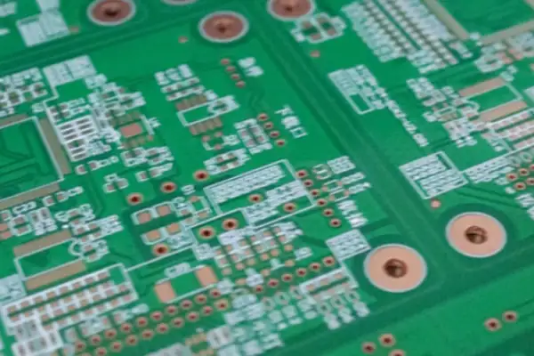
Just last week, a client approached me for a consultation, bringing along some HASL-finished PCB samples; they were in the process of selecting components for medical equipment. The solder coating on this batch of boards measured approximately 15μm in thickness, and the surface flatness had been controlled to an impressively high standard. Using a magnifying glass, I closely examined the coating distribution along the edges of the solder pads and observed clear evidence of significant progress in modern processing techniques—a stark contrast to the solder accumulation issues we frequently encountered during our experiments in years past.
Regarding the choice between leaded and lead-free finishes, I feel that industry discussions on the subject often tend toward extremes. On one occasion, we conducted comparative tests to assess the impact of varying coating thicknesses on signal integrity. We sectioned the samples into small 10mm × 10mm squares and examined the formation of the Intermetallic Compound (IMC) layer under a high-magnification microscope. The results revealed that the critical factor was not the presence or absence of lead *per se*, but rather the precision with which the process parameters were controlled.
High-frequency applications, in particular, represent a subject that warrants further in-depth exploration. Many people believe that the surface roughness of a Hot Air Solder Leveling (HASL) finish negatively impacts signal transmission; however, our actual testing revealed that once the signal frequency reaches a certain threshold, this impact actually diminishes. This reminds me of a radar project I worked on last year: the team initially insisted on using an Electroless Nickel Immersion Gold (ENIG) process, but after multiple rounds of validation, they ultimately opted for an optimized HASL solution instead.
My perspective on fine-pitch components may be somewhat unconventional. Nowadays, many fabrication plants can control HASL surface flatness to within Ra 1.5μm—a level that is more than adequate for 0.4mm-pitch BGAs. The critical factor is to account for process characteristics during the design phase—for instance, by incorporating sufficient tolerance margins into the pad dimensions.
Speaking of HDI boards, I recall an interesting case involving a smartwatch project team. They were concerned that the high temperatures associated with HASL might compromise the integrity of the micro-via structures. We conducted a comparative experiment and discovered that the root cause of the issue lay in thermal management, not in the surface finish itself.
There is no single “right answer” when it comes to selecting a surface finish. I recently worked on an industrial control project where the team ultimately settled on a moderate coating thickness; this approach successfully balanced solderability requirements with cost-efficiency. The key takeaway is that such decisions should always be guided by the specific lifecycle requirements of the product.
Whenever I hear someone dismiss the HASL process as utterly worthless, I can’t help but chuckle—it makes it sound as if selecting a surface finish were akin to playing a game of Minesweeper. After handling hundreds of different PCB designs, I’ve come to realize that success or failure is rarely determined by the process itself, but rather by how well that process aligns with the specific application scenario. Take standard HASL PCBs, for example: many people recoil at the mere mention of “high temperatures,” fearing the heat will damage the board. In reality, however, the temperature control mechanisms used in modern lead-free HASL processes have become remarkably sophisticated and reliable.
I also recall a smart home project from last year where the client adamantly insisted on using an ENIG finish, arguing that it projected a more “premium” image. However, during the prototyping phase, they encountered persistent issues with low BGA soldering yields, necessitating repeated adjustments to the reflow oven temperature profiles. When they subsequently switched to a HASL solution, the boards passed validation on the very first attempt. The lesson here is that for boards featuring components of standard density, there is simply no need to chase after the extreme flatness offered by finishes like ENIG.
The issue regarding the number of reflow cycles is particularly fascinating. During a test involving a double-sided SMT board, we conducted a direct comparison between two different surface finishes. Our findings indicated that after undergoing three reflow cycles, the ENIG pads did indeed exhibit slightly greater stability; however, the difference was so negligible as to be practically irrelevant. Unless you are designing products for the medical or aerospace/defense sectors—which demand exceptionally rigorous standards—most consumer electronics applications simply do not require such extreme specifications. The most extreme example I’ve ever encountered involved a team that, in an effort to cut costs, opted to use tin-plating even on precision connectors. Consequently, after just a few insertion-and-removal cycles, the plating wore right off. In a scenario where Electroless Nickel Immersion Gold (ENIG) was clearly the appropriate choice, such forced cost-cutting proved to be a false economy—ultimately doing more harm than good.
Regarding the issue of copper dissolution, most mainstream manufacturers today actually pre-incorporate copper elements into their solder alloys. Much like seasoning a dish to establish a flavor base, this approach allows them to control the extent of copper dissolution right at the source. What truly warrants concern, however, are high-speed signal lines that demand exceptionally strict impedance consistency; it is in these specific applications that the advantages of ENIG plating truly come to the fore.
I recently helped a friend redesign a drone flight control board. Originally, I planned to use immersion gold plating, but I found that most of the components on the board were 0805 or larger, and only two QFNs required a slightly higher degree of flatness. In the end, I compromised and used a solution of partial immersion gold plating plus overall tin plating, which reduced the cost by one-third without compromising the effect.
Sometimes, I feel that choosing a surface finish is much like choosing a pair of shoes: a proper fit is far more important than mere aesthetics. There is no need to wear custom-made leather shoes for every occasion; after all, running shoes can get you through a marathon—the key lies in knowing exactly what kind of terrain you’ll be traversing.
I recently had a conversation with a friend who works in circuit design regarding the selection of PCB surface finishes. He mentioned that, nowadays, many people immediately shake their heads in disapproval the moment they hear the term “HASL PCB.” However, I believe this perspective is somewhat one-sided.
I recall a project we undertook last year that involved manufacturing a batch of industrial controllers. At the time, our supplier recommended the HASL process. Initially, I was concerned about issues regarding surface flatness. However, actual testing revealed that modern lead-free HASL technology has matured significantly. The flatness of the solder pads proved entirely adequate for mounting standard components. For instance, when using 0805-package resistors and capacitors, as well as SOIC integrated circuits, our soldering yield rate exceeded 99.2%. The supplier even provided third-party inspection reports demonstrating that the uniformity of the pad thickness was controlled within a tolerance of ±25μm—a level of precision that is more than stable and reliable enough for the vast majority of consumer electronics and industrial control applications.
Some people seem to operate under the assumption that when selecting a surface finish, one must always opt for the most expensive option available. In reality, this approach often leads to a wasteful allocation of resources. It is much like buying clothes: not every occasion calls for a custom-tailored suit. For daily commuting, for example, choosing comfortable and durable casual wear is often far more practical—it saves money while fully meeting functional requirements. By the same token, applying an immersion gold finish to a product designed for indoor use—where temperature and humidity are controlled—is akin to adding gold trim to your everyday casual wear; while it may look flashy, it serves no practical purpose.
I have encountered far too many engineers who, in their pursuit of so-called “high-end specifications,” insist on designating expensive surface finish processes during the design phase. Consequently, the manufacturing cost for the entire batch of PCBs ends up being more than 30% higher than necessary. Yet, in reality, these boards are ultimately destined for use in ordinary household appliances. For instance, I’ve seen the mainboard of a rice cooker utilize an immersion gold finish, even though actual soldering temperature profiles demonstrated that a standard HASL finish could easily withstand the process requirements of three separate reflow cycles. This type of “over-engineering” is akin to equipping a commuter car with a racing engine—it creates a surplus of performance that yields no tangible practical value.
Modern lead-free HASL processes have indeed made tremendous strides in recent years. In particular, advancements in hot air leveling technology have resulted in significantly more uniform solder pad surfaces. While it may not be suitable for chips requiring ultra-fine pitch spacing, for the vast majority of applications, it is more than sufficient. For instance, in the case of microcontrollers utilizing QFP packages (with a pin pitch of 0.65mm or greater), or connectors with pad areas exceeding 0.8mm², the Hot Air Solder Leveling (HASL) process delivers excellent soldering results. Modern HASL lines have also incorporated nitrogen protection technology, which effectively minimizes dross formation and extends the pad’s oxidation-free shelf life to over six months.
Sometimes, the simplest solution proves to be the most reliable. As our veteran engineers often say: the *right* solution is the *best* solution. Take the automotive electronics sector, for example: although the ENIG (Electroless Nickel Immersion Gold) process is more prevalent, certain non-safety-critical modules—such as audio systems—have demonstrated superior mechanical strength when utilizing an improved, high-temperature HASL process. In vibration testing, the rate of solder joint failure for these boards was 15% lower than that observed with the chemical gold plating process.
Of course, every project presents a unique set of circumstances. The key lies in making choices based on actual requirements, rather than blindly following trends or allowing one’s thinking to be constrained by preconceived notions. For instance, medical devices demand rigorous long-term reliability, while communication base stations prioritize minimizing high-frequency signal loss; it is in these specific scenarios that more advanced surface finish processes should be given priority.
I believe the most critical aspect of making technical decisions is maintaining an open mind. One should not dismiss the value of a particular process simply because it is labeled an “economical option.” After all, in the realm of actual manufacturing, reliability and cost-effectiveness often carry far more weight than the mere label of being “high-end.” This principle is even evident in the aerospace industry, where mature, proven processes are frequently employed for non-critical components—relying on rigorous process validation to ensure overall system reliability—rather than blindly chasing the very latest technologies.
While recently organizing some notes on PCB surface finishes, I noticed an interesting phenomenon: many people today—upon hearing the term “HASL PCB”—instinctively dismiss it as an obsolete technology. In reality, such a perspective is quite one-sided.
Last year, we had a medical device project where the initial plan called for using the Electroless Gold (ENIG) process for the circuit boards. However, due to cost considerations, we decided to experiment by substituting lead-free HASL for a portion of the non-critical circuit boards. During the testing phase, we discovered that the soldering yield rate for this batch of HASL boards was actually significantly higher than that of the gold-plated boards. Our senior workshop technicians explained that this was because the HASL surface itself possesses inherent flux-like properties, making it particularly well-suited for high-volume manufacturing environments.
However, there is one important detail to note here: not every manufacturing facility is equipped to execute HASL processing with the high degree of precision required for demanding applications. I once visited a small, workshop-style PCB facility where the temperature fluctuations in their solder pot exceeded 20 degrees Celsius. Under such conditions, the boards produced could not even guarantee the most basic level of uniformity. Later, when we partnered with a professional manufacturer, they meticulously recorded copper content variations during every shift—even adjusting the air knife angles based on board thickness. It is precisely these minute details that constitute the key to quality.
Nowadays, when many engineers deliberate over whether to opt for lead-free hot air solder leveling (HASL), they tend to focus their attention solely on thickness specifications. I, however, believe it is far more critical to scrutinize the supplier’s ability to control solder composition; I have witnessed far too many instances where excessive impurities led to solder joint embrittlement. Occasionally, suppliers present impressive inspection reports, yet during actual production, they fail to implement even basic anti-oxidation measures—engaging in such partnerships carries significant risk.
In fact, there is a very intuitive method for assessing the quality of a HASL finish: examining the state of the solder coating along the board’s edges. A high-quality HASL finish should be as smooth as a mirror; if there are noticeable irregularities or the surface appears dull, it is time to re-evaluate the supplier’s process capabilities. We once rejected an entire batch of boards because tiny solder beads appeared along the edges—a defect we later traced back to an improperly calibrated air knife pressure setting.
Recently, while working on an automotive electronics project, I observed a new trend: some manufacturers have begun combining HASL with other surface finishes. For instance, they might apply Electroless Nickel Immersion Gold (ENIG) to BGA areas while using HASL for the remaining sections of the board. This approach effectively ensures reliability while simultaneously keeping costs under control. Such a flexible and pragmatic mindset holds far greater practical value than the mere pursuit of high-end processes for their own sake.
In the field of medical electronics, attention often focuses on complex algorithms;
After years of navigating the hardware industry, I’ve observed an interesting phenomenon:
As a practitioner in the circuit board manufacturing industry, I am keenly
- 중소규모 배치 생산 전문가
- 고정밀 PCB 제작 및 자동화된 조립
- OEM/ODM 전자 프로젝트를 위한 신뢰할 수 있는 파트너
영업 시간: (월~토) 9:00~18:30