
From Novice to Expert: Sharing My Experience in Pin Header PCB Selection
As an electronics enthusiast, I’ve come to understand firsthand the impact of
Whenever I disassemble an electronic device and see those dense clusters of tiny white text, I often find myself wondering: what on earth is the point of all this? To be honest, when I first started working with circuit boards, I assumed that white layer was nothing more than a decorative element. It wasn’t until I began doing my own hands-on soldering that I realized its importance far exceeded anything I had imagined.
A friend of mine once chose to order boards *without* silkscreen printing just to save a few dollars. The result? During soldering, he accidentally reversed the polarity of a diode, rendering the entire board completely useless. That costly lesson taught me that even the smallest details deserve our utmost attention.
Many people assume that the silkscreen on a circuit board serves merely as a marker for the factory assembly line; in reality, it functions more like an instruction manual, guiding you on how to correctly assemble and maintain the device. Imagine a scenario without these labels: a repair technician might have to spend an exorbitant amount of time individually measuring every single component. With clear, well-placed markings, however, work efficiency can be boosted dramatically.
I remember the first time I designed a PCB, I set the silkscreen font size far too small; when the manufacturer printed it, the text was almost illegible. Since then, I’ve learned to meticulously double-check these seemingly trivial details before submitting my design files for fabrication.
Nowadays, some smart devices on the market—in pursuit of a sleek, minimalist aesthetic—have completely eliminated surface markings. While such designs may look beautiful, they create significant difficulties for subsequent maintenance. I once disassembled a high-end audio system where the internal components were packed tightly together with absolutely no identifying labels, making the entire repair process incredibly arduous.
Effective silkscreen design requires careful consideration of the user’s actual usage scenarios—for instance, utilizing abbreviations and symbols on space-constrained boards while ensuring that critical information remains clearly visible. This demands that the designer possess a deep understanding of manufacturing processes, rather than simply haphazardly cluttering the board with text. With technological advancements, laser engraving is gradually replacing traditional ink printing methods. This technique offers higher precision and superior durability, making it particularly well-suited for miniaturized devices; however, cost remains a significant barrier to its widespread adoption.
Truly excellent silkscreen printing should ensure that—even years later, when a device requires maintenance—technicians can still quickly grasp the original design intent. This necessitates that we consider the needs of the product’s entire lifecycle right from the design phase.
Whenever I see those tiny white markings on a circuit board, I find them particularly fascinating. These elements may appear inconspicuous, yet they carry the entire board’s identity information. I have observed many engineers spending vast amounts of time during the design phase debating component placement, only to treat the silkscreen layer as a dispensable, purely decorative element. In reality, these markings serve as the critical bridge connecting the design concept to its practical application.
I recall an instance while debugging a complex control board late one night; the production line was waiting for this specific board to undergo testing. Amidst a dense array of components, I relied on the silkscreen markings to quickly pinpoint the problematic area. Without these clear labels, it might have taken me an additional half-hour just to trace the signal paths. In moments like these, you truly appreciate just how significantly effective silkscreen design boosts work efficiency. This is especially true when troubleshooting high-frequency signal interference, where silkscreen-labeled test points can directly guide a probe to make precise contact, thereby preventing accidental contact with adjacent components that could lead to measurement inaccuracies.
Nowadays, many young engineers tend to pursue a minimalist design aesthetic, often attempting to compress the silkscreen layer until it is barely visible. They reason that since the markings aren’t strictly necessary during mass production, why waste effort on them? However, the lifecycle of an electronic product extends far beyond the production line; from initial prototype debugging to long-term maintenance, the silkscreen layer continues to play a vital role. I have handled numerous repair cases where ambiguous silkscreen markings caused the time required for repairs to multiply exponentially. For instance, when repairing industrial controllers, faded silkscreen labels can turn the process of replacing a fuse or relay into a guessing game—potentially even leading to secondary failures caused by misidentifying pin assignments.
Recently, while reviewing a friend’s IoT module design, I noticed that he had annotated the current tolerance for each interface directly onto the silkscreen layer. This thoughtful approach allows subsequent assembly personnel to quickly determine the appropriate power configuration, thereby avoiding common wiring errors. What appeared to be a mere few extra minutes spent during the design phase ultimately saved significant potential time costs for the entire project. He also specifically utilized distinct icons to differentiate between analog and digital interfaces, a measure that helps minimize the risk of confusion, even when the device is being handled by non-specialists.
A truly efficient PCB design must take into account the requirements of the entire product lifecycle. From the component placement stage to final maintenance, every step of the process benefits from clear silkscreen markings. It is akin to equipping the circuit board with a navigational map, enabling everyone who interacts with it to carry out their work smoothly. For instance, during the SMT placement phase, component designators and polarity markers effectively prevent incorrect orientation; meanwhile, during quality inspection, version numbers and date codes serve as crucial clues for tracing the quality of specific production batches. Whenever I see those tiny white markings on a circuit board, I find myself wondering just how important this stuff really is. Many people view the silkscreen layer on a PCB as nothing more than a decorative element, but in reality, it plays a crucial role in ensuring the entire assembly process runs smoothly. I remember when I first started out in PCB design, I completely underestimated the significance of the silkscreen layer. The result? The first batch of prototype boards we received back gave us a massive headache. Components were installed backward left and right—especially polarized parts like capacitors and diodes. If the markings on the silkscreen aren’t clear enough, workers have to go through the tedious process of checking each component individually with a magnifying glass; this not only kills efficiency but also makes errors far more likely.
Designing the silkscreen layer actually requires a great deal of experience. For instance, handling the layout around solder pads demands extreme caution. Sometimes, in an effort to save space, designers will place text right up against the pads; however, this can cause the ink to bubble when heated during the soldering process. The most extreme case I’ve ever witnessed involved a silkscreen layer printed directly *over* the solder pads—rendering it impossible for the components to adhere at all. Since then, we’ve made it a habit to leave a sufficient safety clearance around all conductive areas. While this might consume a little extra board real estate, it is infinitely preferable to having to rework the boards later.
Another easily overlooked aspect is the orientation of the text. I’ve noticed that many engineers like to arrange text in various directions, believing it helps conserve space. However, assembly line workers need to be able to identify component locations quickly; if the markings for every component are oriented differently, it actually *increases* the time required for identification. We now strictly adhere to a consistent left-to-right text orientation—maintaining this uniformity even for polarized components like diodes. Although this entails sacrificing a tiny bit of layout flexibility, the resulting boost in assembly efficiency is significant.
Speaking of polarity markings, I’ve found that the most practical approach is to use graphic symbols rather than pure text. For example, using a simple triangle symbol to denote the anode and cathode of a diode is far more intuitive than writing out a string of English abbreviations. This is particularly true for smaller circuit boards, where simple graphics are often much easier to recognize than text. On one occasion, we designed a high-density board where the use of icon-based polarity markings allowed us to complete the entire surface-mount assembly process nearly half an hour faster than anticipated.
Ultimately, the silkscreen layer serves as the circuit board’s instruction manual. By taking the time during the design phase to view things from the assembler’s perspective, you can often preempt a great deal of unnecessary trouble. Nowadays, after I finish laying out a board, I always switch to the silkscreen view to simulate the actual assembly scenario; this simple habit has saved me from countless detours and headaches.
Those tiny white markings on a circuit board might look inconspicuous, but for the assembly workers, they serve as the essential roadmap guiding their way. I’ve seen far too many cases of rework caused by issues with silkscreen printing—it’s truly heartbreaking to watch workers poring over boards with magnifying glasses just to identify component orientation.
Nowadays, quite a few manufacturers are beginning to experiment with inkjet technology for this stage of the process. Spraying ink directly onto the board sounds simple enough, right? However, in practice, there are numerous factors to consider. For instance, ink adhesion is a critical point—the surfaces of certain solder mask materials are simply too smooth for the ink to properly adhere.
A client once came to me with a sample board, complaining that the silkscreen markings rubbed off at the slightest touch; we later discovered the issue lay in their choice of solder mask material. This experience made me realize that selecting the right combination of materials is far more important than simply chasing after the latest technology.
Traditional screen printing certainly has its limitations, but its strength lies in its stability and reliability. While inkjet technology offers flexibility, the cost of the specialized inks required is often prohibitive, and it imposes much stricter requirements on the production environment.
What concerns me most, however, is the handling of details during the design phase. Many people treat the PCB silkscreen as a mere afterthought—something to be slapped on at the end with little regard for placement. The truly professional approach, however, involves integrating these markings into the layout process from the very beginning, ensuring adequate spacing and proper positioning.
I recall seeing a board once where the component identifiers were squeezed tightly between the solder pads; during assembly, workers had to repeatedly verify component orientation, significantly slowing down the production pace. Such details may seem trivial, yet they have a direct impact on manufacturing efficiency.
Ultimately, the choice of process depends on specific requirements. For high-volume production runs, traditional methods may prove more economical; conversely, if designs undergo frequent revisions, the flexibility of inkjet technology truly shines. The key is to identify the solution that best suits your specific needs, rather than blindly chasing after the latest technological trends.
I’ve recently noticed a particularly interesting phenomenon: when discussing PCB design, many people tend to focus their attention almost exclusively on the circuit layout, while rarely giving a second thought to the small white text printed on the board itself. Yet, these seemingly inconspicuous printed markings are, in fact, the most human and soulful element of the entire circuit board.
I remember the first time I held a PCB I had designed myself; what delighted me most wasn’t just that the circuitry functioned correctly, but seeing those crisp, clear identifiers on the silkscreen layer. It felt akin to naming one’s own child—suddenly, those cold, inanimate electronic components were imbued with a sense of life. Especially after I added my own signature to a corner of the board, that PCB was instantly transformed into a truly unique and personal work of art. Some manufacturers are now starting to offer full-color silkscreen services—a truly exciting development. Although the costs are still relatively high at the moment, I can hardly wait to give it a try. Just imagine: on a circuit board, you could not only label component locations but also use different colors to distinguish functional zones, or even incorporate small graphic designs. This completely shatters the traditional stereotype that PCBs must be either black or green.
When it comes to the practicality of circuit board silkscreening, I believe the most crucial aspect is striking a balance between aesthetics and functionality. I’ve seen far too many designs where, in pursuit of a “cool” aesthetic, the text is printed so small that it ends up looking like an illegible blur on the production line. Conversely, there are designs that are overly conservative—featuring vast expanses of blank space yet containing nothing but a few massive, oversized characters. Good silkscreen design should be akin to excellent UI design: maintaining visual appeal without compromising usability.
I particularly enjoy observing the differences in silkscreen craftsmanship across various manufacturers. Some can print tiny 0.2mm text with razor-sharp precision, while others appear somewhat crude in their handling of fine details. These subtle nuances often serve as a barometer of a manufacturer’s commitment to quality. In fact, when selecting a supplier, simply examining the silkscreen quality on their sample boards can often give you a 70 to 80 percent accurate assessment of their capabilities.
As the demand for personalization continues to intensify, I believe that in the future, PCBs will evolve into something more akin to bespoke works of art. I recently saw a maker who had silkscreened an anime character onto a Raspberry Pi expansion board; while it offered absolutely no functional benefit, it undeniably gave the entire project a unique and distinctive identity. This trend reminds me of the evolution of mobile phone cases—from purely protective shells to vehicles for personal expression. After all, who would still be content with a completely featureless circuit board these days?
That said, no matter how flashy the silkscreen design may be, it must ultimately be built upon a foundation of solid technical fundamentals. The worst designs I’ve encountered are those where polarity markers are obscured by the shadows of the components themselves, or where critical information is printed in areas destined to be covered by heat sinks. These details may seem trivial, but they serve as the ultimate test of a designer’s accumulated experience.
Occasionally, when browsing through circuit boards from a decade ago, I find their silkscreen styles particularly fascinating—the fonts were bolder and more rugged, and the layouts felt much more spontaneous. Today’s designs, by contrast, have become increasingly refined and standardized; this very process of evolution tells a compelling story in itself. Perhaps another ten years from now, when we look back on today’s full-color silkscreen technology, we will view it as something distinctly characteristic of this specific era.
Ultimately, the silkscreen serves as the circuit board’s signature. It need not steal the spotlight, but when executed just right, it can imbue the entire board with a unique sense of character. The next time you design a PCB, consider devoting a little extra thought to this aspect; you might find the process far more enjoyable than you imagined.
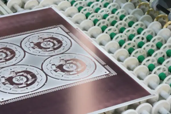
I’ve always found those small white markings on circuit boards quite fascinating. Although they may appear inconspicuous, these silkscreen prints actually harbor a surprising number of intricacies. I recall one instance while debugging a board where I discovered a resistor value had been mislabeled; I spent the better part of a day troubleshooting before finally pinpointing the issue. Later, while chatting with a veteran technician at the factory, I learned that this error was caused by a misalignment during the screen-printing process—specifically, the ink hadn’t fully dried before the stencil was lifted.
Nowadays, many manufacturers—in an effort to cut costs—render their silkscreen markings incredibly small. I once encountered a board with such minuscule characters that a magnifying glass was required to decipher them. Such a design is nothing short of a nightmare for maintenance personnel. In reality, a circuit board’s legibility is far more critical than its aesthetic appeal; after all, these markings are intended for human eyes, not for machines.
The choice of ink itself is also a matter of some nuance. Some manufacturers, in their pursuit of superior adhesion, opt for exceptionally rigid inks—only to find that these materials are prone to cracking. I personally prefer materials that possess a certain degree of resilience; this ensures that even if the board warps slightly under heat, the markings won’t easily flake off.
I recently worked on a project that gave me a real headache: the client insisted on cramming over a dozen lines of explanatory text onto a tiny circuit board. I spent a considerable amount of time explaining to them that silkscreen printing isn’t a panacea, but we eventually reached a compromise: we moved the detailed explanations into the accompanying documentation, leaving only the essential identifiers on the board itself.
Ultimately, circuit board design is an art of making trade-offs. The silkscreen layer, while seemingly simple, requires balancing a multitude of factors—including printing precision, ink characteristics, and the practical context of the board’s usage. Sometimes, the simplest designs prove to be the most practical; those flashy, purely decorative text elements often serve no real purpose other than driving up costs.
One of the smartest approaches I’ve seen involves designating a specific “information zone” along the edge of the circuit board to consolidate key details—such as the version number and date—in a centralized layout. This arrangement facilitates easy viewing without interfering with the board’s routing; more importantly, it ensures that maintenance technicians can instantly locate the information they need at a single glance.
Those white markings on circuit boards really are quite intriguing. I’ve even witnessed someone scraping away at the silkscreen-printed component symbols with a fingernail for ages—only to find that the markings remained stubbornly intact. Behind this durability lies a contest between ink formulations and curing processes—some manufacturers, in an effort to cut costs, will shorten the curing time.
I recall an interesting phenomenon I observed once while helping a friend repair an audio amplifier board: the clarity of the silkscreen printing varied significantly among boards from the very same production batch. I later learned that this was caused by uneven tension in the mesh screens during the silkscreen printing process. This experience made me realize that even the most mature manufacturing processes are subject to inherent variability.
Nowadays, many engineers like to make their company logos exceptionally large. However, oversized graphics consume valuable space that could otherwise be used for routing traces. Personally, I believe that when it comes to identification markings, “just enough” is sufficient.
Direct inkjet technology has indeed introduced fresh perspectives to the industry. However, as things stand, traditional silkscreen printing still retains an advantage in terms of cost control. After all, not every product requires identification markings with micron-level precision.
During a factory tour on one occasion, I noticed a specific detail: whenever operators switched to a different ink color, they would thoroughly clean the print heads using a solvent. This seemingly simple step has a direct impact on the overall print quality.
There is actually some debate regarding the use of physical masks. Some argue that digital workflows allow one to bypass the physical masking stage entirely. Yet, in actual practice, many veteran technicians still place greater trust in the level of control afforded by physical film negatives.
I have recently noticed a growing trend: an increasing number of consumer electronics products are adopting a design featuring dark-colored circuit boards paired with light-colored silkscreen printing. While this visual contrast certainly enhances the product’s aesthetic appeal and perceived quality, it also imposes stricter requirements on printing precision.
In fact, there is a simple method for assessing the quality of silkscreen printing: use a magnifying glass to examine the edges of the characters for any roughness or fraying. Smooth, clean edges typically indicate superior adhesion.
Ultimately, the markings on a circuit board serve as the product’s identity card. They must be neither so rudimentary as to hinder maintenance, nor so elaborate as to drive up costs. Striking this balance requires the designer to possess a deep understanding of the manufacturing process.
Sometimes, spotting slightly misaligned component symbols actually evokes a sense of warmth—it serves as a reminder that this product is the result of genuine human involvement in production, rather than merely a flawless artifact of total automation.
Whenever I look at the tiny white text printed on a circuit board, I find it particularly fascinating. These markings might seem inconspicuous, but in reality, they are as vital as the product’s own ID card.
I have witnessed far too many blunders caused by a disregard for detail. On one occasion, while helping a friend repair an audio amplifier board, I spent ages searching for the model number—only to discover later that the manufacturer had printed the characters too close to the heat vents; the high temperatures had effectively baked the text until it was completely illegible. This issue could have been entirely avoided had the actual operating environment been taken into account during the design phase.
Nowadays, many engineers tend to focus their attention primarily on circuit performance—and while that is certainly not wrong—I believe that visual markings and labeling deserve equal consideration. After all, a product is designed to be used by people; it isn’t simply meant to be sealed inside a “black box” and forgotten.
I recall a smart home project we worked on last year where we invested a great deal of effort into the circuit board silkscreening. We didn’t just fine-tune the placement of the characters; we also specifically selected heat-resistant ink materials. Although this added slightly to the production costs, the client feedback was overwhelmingly positive—they noted that during maintenance, key information could be identified at a glance. That kind of investment truly paid off.
Speaking of character printing, I believe the most easily overlooked aspect is color consistency. While this might sound like a simple matter, executing it in practice requires exceptional diligence; different batches of ink can exhibit subtle variations. We consistently require our manufacturers to provide color samples for comparison, ensuring that the overall visual aesthetic remains uniform.
In fact, many factories today are actively elevating their technical standards in this area—for instance, by adopting high-precision printing equipment to ensure that even the tiniest characters remain clearly legible. For us designers, this is excellent news, as it means we can now realize even more complex and sophisticated design concepts.
I have always maintained that a truly excellent product must be impeccable both inside and out. While circuit performance establishes the product’s baseline quality, the meticulous handling of details—such as silkscreen printing—often determines its ultimate potential. After all, the elements that users directly perceive and interact with are precisely these tangible, visible components.
I am currently working on an industrial controller project, and I’ve taken particular note of the rigorous demands placed on silkscreen durability for equipment intended for outdoor use. We are currently testing a new type of UV-resistant ink in the hope of resolving the issue of text fading caused by prolonged exposure to sunlight. This seemingly minor detail may very well prove to be one of the product’s standout features. Ultimately, the markings on a circuit board are not merely decorative; they serve a vital function in conveying information. We must tailor our design strategies to the specific application scenarios to create products that are both aesthetically pleasing and functionally practical.
I have always found that layer of white printing on a circuit board particularly fascinating. When I first started out in electronics design, I completely overlooked these details; it wasn’t until I was debugging a board one day that I realized the silkscreen layer plays a far more critical role than I had imagined. Those seemingly simple markings actually conceal the designer’s ingenuity.
I remember nearly making a rookie mistake the first time I designed a board myself. I made the reference designators for the resistors incredibly small, thinking, “As long as *I* can understand them, it’s fine.” The result? The soldering technician had to spend ages hunting with a magnifying glass just to barely make them out. I later realized that the silkscreen isn’t just a personal sticky note for the designer; it serves as a guide for everyone who interacts with the board. Effective silkscreen markings should be like road signs—clear and direct—allowing anyone to grasp key information at a glance.
Nowadays, when designing, I pay special attention to how polarized components are marked. I once encountered a situation where an entire batch of products had to be reworked because the polarity markings on the capacitors were ambiguous. In reality, simply adding a small dot or a shaded area at the negative terminal location is enough to prevent such issues. Sometimes, it is the most fundamental design details that are most prone to going wrong.
Recently, while refining our company’s silkscreen standards, I observed an interesting phenomenon. Many engineers are in the habit of tucking the version number away in an inconspicuous corner, yet in actual production, this information is critically important. Assembly line workers rely on it to verify material batches, and maintenance personnel need it to identify specific circuit revisions. Consequently, we standardized the placement of the version number, positioning it prominently along the edge of the board and adding a QR code that links directly to the design documentation.
However, when it comes to silkscreen, more complexity isn’t necessarily better. I have seen boards where the component outlines were drawn with excessive detail, which actually compromised soldering quality—particularly when characters were positioned too close to the solder pads, increasing the risk of cold joints. My current preference is to use concise symbols paired with unambiguous reference designators; this approach ensures readability while leaving ample clearance for manufacturing processes.
What moved me most was an experience I had while repairing a piece of equipment that was ten years old. Upon opening the chassis, I discovered that the silkscreen markings on the circuit board were still perfectly legible. Those slightly raised white characters felt like a time capsule, preserving the traces of the original designer’s thought process. This dialogue across the span of time gave me a renewed appreciation for how seemingly auxiliary design elements can, in fact, hold a value that endures far longer than one might imagine. Whenever I unbox a newly arrived circuit board, the first thing I check is the silkscreen layer. Those small white characters are as vital as the board’s very own ID card.
I recall a time when I was helping a friend modify an old project board; the markings on it were so worn down that I had to rely on guesswork to figure out which resistor belonged in which position—a process that ended up wasting an entire afternoon.
Nowadays, I make it a habit to keep the height of my silkscreen text around 1 millimeter. This size strikes a good balance: it doesn’t take up excessive space, yet it remains clearly legible throughout the manufacturing process.
Many people view the silkscreen merely as a decorative element; in reality, however, it plays a critical role in subsequent debugging and maintenance.
I once encountered a board designed by someone else where the component designators were placed directly in the center of the solder pads—only to be completely obscured once the components were soldered in place. It is precisely these kinds of details that demand careful attention.
Regarding line width, I generally avoid going any thinner than 0.12 millimeters. Any finer than that, and the ink tends to print discontinuously—especially on boards with slightly uneven surfaces.
Ultimately, what matters most to me regarding the silkscreen layer is its ability to accurately convey the design intent, rather than simply striving for the smallest possible dimensions.
An experienced engineer once told me that effective silkscreen markings should allow a person to grasp the circuit’s functionality at a single glance, rather than forcing them to hunt for information with a magnifying glass.
I’ve noticed that there is significant variation in how different manufacturers execute the silkscreen process; some struggle to print even a 0.15-millimeter line width without blurring, while others can clearly reproduce lines that are even finer.
Recently, while designing a motor driver board, I deliberately made the markings for the power components larger than those for the signal circuitry. This ensures that during assembly, workers can quickly and easily distinguish between the different functional zones.
Sometimes, to make room for critical markings, I would rather adjust the component layout than compromise the clarity of the silkscreen—after all, the usability of the entire board hinges on it.
In truth, the ideal silkscreen is one that maintains technical precision while simultaneously allowing the user to sense the thoughtfulness behind the design; finding that perfect balance requires continuous refinement and adjustment across various real-world projects.
As an electronics enthusiast, I’ve come to understand firsthand the impact of
Why is green the universal choice for circuit boards? Behind this seemingly
As a hardware entrepreneur, I often see teams fall into a trap
- 중소규모 배치 생산 전문가
- 고정밀 PCB 제작 및 자동화된 조립
- OEM/ODM 전자 프로젝트를 위한 신뢰할 수 있는 파트너
영업 시간: (월~토) 9:00~18:30