
5G Base Station PCB: High Frequency Design, Manufacturing Challenges, and Reliable Solutions
When we talk about 5G, we often only focus on the grand
Many people think that the most critical component of an electric vehicle is the battery or motor. This is certainly true. But after working in circuit board design for so many years, I understand a truth: the thing that really determines whether your car can be “charged” with electricity is actually quite inconspicuous – it is the circuit board in the fast charging pile that is responsible for handling large currents. This thing looks like a green board with a few lines.
I’ve seen too many embarrassing situations caused by problems with this board. Last summer, a friend drove his new car to a new supercharging station to experience the feeling of high-speed recharging. As a result, within a few minutes of plugging in the gun, the screen went black and then the entire pile went out of power, which made him extremely depressed and delayed his subsequent schedule. Later, when we chatted, we learned that several newly installed equipment in that station had experienced similar problems. The root cause was that the internal PCB responsible for current transmission could not keep up with the heat dissipation during continuous high-power operation, and the circuit design was a bit conservative.
This reminds me that many manufacturers are now promoting the power and speed of their charging piles. But to be honest, if the basic hardware that supports these functions is not up to par, then no matter how beautiful the parameters are, they are just words on paper. A qualified EV Charger PCB, especially the one used in DC fast charging equipment, must be able to withstand high-intensity current impacts for a long time and remain stable.
There are actually many ways to do this. For example, the Heavy copper PCB we often talk about is a solution. It increases the current carrying capacity and reduces heat generation by increasing the thickness of the copper layer. However, this also brings process challenges. For example, the etching precision is more difficult to control and the cost is higher. Not all factories can do it well.
I think there is a bad tendency in the industry that everyone is too focused on “peak performance” and ignores long-term reliability. A circuit board may have passed the test of instantaneous high current during design, but in actual operation it needs to face frequent starts and stops day after day, ambient temperature changes and various unforeseen voltage fluctuations, which are the real tests.
Take a project I participated in as an example. In order to design supporting fast charging equipment for a dedicated site of a logistics fleet, when we selected the core PCB, we did not blindly pursue the highest current specifications, but focused on its performance in different seasons, especially in the humid and hot weather in the south. We even simulated a continuous working scenario for more than twelve hours to repeatedly test its temperature rise.
The results proved that this idea was correct. The equipment at the site had been running for more than two years and the failure rate was far lower than the industry average. Although the initial investment was slightly higher, it saved a lot of maintenance costs and downtime losses in the long run.
Therefore, in my opinion, when discussing charging technology, we cannot just focus on the energy density of the battery or the voltage platform of the vehicle. The quality of the charging pile itself, especially these “heart” level components, is the key link that determines the user experience. A good PCB allows energy to flow efficiently and safely, while a defective board may paralyze the entire system at any time.
This industry is still developing rapidly. In the future, there will definitely be higher power requirements and more complex technology integration. However, the solidity and reliability of basic components will always come first. Otherwise, building more charging points may just create more potential troubles.
I recently discovered an interesting phenomenon when chatting with several friends who are engaged in hardware design: many people subconsciously think that the circuit board in an EV charging pile is particularly high-end and complicated when they mention it. In fact, there is a big misunderstanding here – not all PCBs in charging piles are so mysterious.
Let’s take our most common home slow charging station as an example. The circuit board used inside this device for slowly replenishing power for electric vehicles is actually not much different from the control boards of many smart home appliances. They handle AC input and do not require complex power conversion, so the requirements for boards are more towards stability and integration.
I have seen some manufacturers use extremely thin copper foil on these boards in order to save costs. As a result, after a period of use, the interface part begins to have poor contact. This is not because the power is insufficient, but because the mechanical stress caused by long-term plugging and unplugging slowly causes micro-cracks in those thin traces.
What’s really interesting is that when you switch from slow charging to fast charging, the entire design logic is completely different. At this time, what you face is no longer a simple current conduction problem, but how to make a board withstand a huge energy impact in a short period of time.
An engineer I know once complained to me that they tested a sample of a fast charging pile and found that after half an hour of continuous high current operation, the temperature in some areas on the board was so high that it could fry an egg. Later, when it was disassembled and analyzed, it was discovered that the problem was that the copper foil of ordinary thickness simply did not have time to disperse the heat evenly, resulting in local overheating.
This reminds me of another common misconception: Many people think that just making the copper thicker will solve all problems. In fact, in a high-frequency switching environment, the skin effect of current will cause most electrons to only flow on the surface of the conductor. Even if you use thicker copper, the middle part will basically be idle. This is purely a waste.
What really needs attention is how to optimize the shape and layout of the traces based on the actual distribution of current. Sometimes a properly designed wide flat trace is much more effective than casually thickening the overall copper layer.
Another thing that is easily overlooked is the difference in performance under different climate conditions. I once saw a batch of charging piles in a southern coastal city that had been used for less than a year. The inside of the casing was full of traces of water vapor corrosion. Although the motherboard had been treated with three-proof treatment, green rust still appeared on the power interface.
This shows that it is not enough to rely solely on the performance of the board itself. The protective design and daily maintenance of the entire system are equally important. After all, these equipment will be exposed to wind and sun outdoors for many years.
Nowadays, many manufacturers like to promote the high-grade heavy copper plates they use or the complex multi-layer designs they use. But I think what users really care about may not be these technical parameters but whether they can charge stably after plugging in the gun, whether the numbers on the screen will jump around, or whether they dare to continue using it on rainy days.
At the end of the day, good design should be such that people cannot feel the existence of the design. It should work silently in the background without being in the limelight and without losing its reputation. Those solutions that talk about various professional terms all day long often expose more unexpected problems in actual use.
So next time when you see a charging pile’s promotional materials printed with various technical indicators, you might as well ask: How much can these data be maintained after three years of use?
I recently discovered an interesting phenomenon while studying the design information of some electric vehicle fast charging stations. Many people think that simply increasing the power number will solve the problem of slow charging. In fact, that’s not the case at all.
The key factor that really determines whether a fast charging station can stably output 600kW of power is often hidden in the most inconspicuous places – those thick copper PCB boards that carry huge currents. I have seen many design cases where engineers arranged the components densely in pursuit of higher power density but ignored the most basic heat dissipation issues.
Once I talked about this topic with a friend who makes charging equipment, and he told me that they had tested EV Charger PCBs with different specifications, and the performance differences in actual operation were astonishingly large. For those boards with ordinary designs, the temperature will rise sharply when working under high load for a long time, causing the entire system to have to run at a reduced frequency. The final actual charging speed may not even reach half of the nominal value.
The truly excellent heavy copper PCB design considers not only the current carrying capacity but also how to distribute the heat evenly and dissipate quickly. This requires planning the heat flow path during PCB layout and sometimes even adding special heat dissipation structures at key locations.
I have observed some devices on the market that claim to support ultra-fast charging and found that their power is often unstable in actual use. The user looked at the 600kW figure displayed on the screen and thought it would be fully charged in a few minutes. However, after waiting for half an hour, he discovered that the actual charging speed was far from expected.
The problem often lies in the details. For example, if the copper thickness or width of the trace between the power conversion module and the battery interface is not enough, it will become a bottleneck of the entire system. Even if the front-end power supply can provide sufficient power, it cannot be effectively delivered to the battery.
Another point that many people tend to overlook is that the performance of PCBs will vary greatly in different seasons and temperatures. The conductivity of materials will change in high-temperature environments in summer. If sufficient margin is not left during design, various strange problems may easily occur.
A good design should take these variables into consideration and make corresponding adjustments in material selection and circuit layout to ensure stable operation in various environments.
After all, the development of electric vehicle fast charging technology should not only look at the superficial power figures, but also pay attention to the basic technologies that support these figures. The knowledge of materials science, thermodynamics and electromagnetism behind a seemingly simple PCB board may be much more than we imagine.
Next time you see a charging station advertising that it supports ultra-high power fast charging, you might as well ask what kind of circuit board design they use. Maybe the answer will give you a new understanding of this technology.
I recently discovered an interesting phenomenon. Many people are particularly superstitious about thick copper when it comes to PCB boards in fast charging piles for electric vehicles. It seems that the thicker the copper foil, the more powerful it will be, and the performance will be absolutely no problem. This is actually a big misunderstanding. I have encountered this problem in many EV Charger PCB design projects. Engineers piled materials together, and the result was expensive and difficult to make, and the performance was not necessarily stable.
You may not know that there is a link in the PCB manufacturing process called etching. To put it simply, the unnecessary copper on the circuit board is removed through chemical methods, leaving the circuit we designed. When your copper layer is particularly thick – such as the often-called Heavy copper PCB – the process of “removing excess copper” will become particularly troublesome. When the potion corrodes copper, it will not only corrode the parts you don’t need downward, but also corrode some “sideways”. This is called the side corrosion effect. The fatter your copper layer, the more serious the lateral erosion will be.
Imagine that you have drawn a thin wire to transmit precise control signals. As a result, due to lateral erosion, this line was “gnawed” away a little more from both sides by the medicine, making it narrower. As soon as the line width changes, the resistance changes, and the impedance characteristics of the entire circuit are completely messed up. For devices such as charging piles that require precise control of power and communication, the result of “a slight mistake” may be low charging efficiency or even communication errors. Therefore, simply pursuing thickness sometimes leads to burying the ground for one’s own products.
I have seen many cases where designers used ultra-thick 8-ounce or even 10-ounce copper layers for power paths in order to pursue high current-carrying capacity, which of course can carry larger currents. But at the same time, the fine lines on the board responsible for signal processing also suffered due to the same etching process, and the yield rate plummeted. In the end, the cost of the entire board soared, but its reliability was compromised.
So what to do?
I think the smarter approach is not to create a “one size fits all” unified thick material, but to “regulate by zoning.” For places that really need to withstand large currents, such as the main path of the power module, you can use thick copper strips or even embedded copper blocks, which is no problem. But those areas responsible for logic control and protocol communication should be handled with conventional or even more sophisticated lines. It is technically possible to have multiple copper layers of different thicknesses on one board at the same time.
In the final analysis, engineering is not about who can use more powerful materials, but who can find the optimal solution within various constraints. Heat dissipation, insulation, current carrying capacity, signal integrity, and cost control all have to be considered together. Next time you think about how to design a charging pile board, don’t just think about thickening it. Think more about how to make the most of every part.
I have always felt that many people have misunderstandings about the design of electric vehicle charger PCBs. They always think that if the copper is thickened, everything will be fine. This idea is actually quite one-sided. If you think about it, on a PCB, the paths of current are not evenly distributed. Some lines need to carry large currents to drive core modules or cooling fans, while others only transmit weak signals. If the entire board is made of thick “heavy armor”, the cost will soar, the manufacturing process will also become extremely complicated, and the yield rate will be difficult to guarantee.
I have seen many design cases where blind pursuit of overall copper thickness resulted in big losses in the reflow soldering process. Those thick copper layers are like small heat sinks soldered to the board. When the entire board passes through the high-temperature furnace, the heat will be quickly absorbed by them, causing the temperature of the surrounding solder joints to not rise, forming so-called cold solder joints. Especially for those precision BGA chips, if the solder ball at the bottom is not completely melted, the result will be bad contact with bad equipment, which can drive people crazy when troubleshooting.
So what’s the smarter thing to do now? It is to carry out zoning design and only work on where it is really needed. For example, the “main roads” connecting the main power switch tubes and filter capacitors must use thick copper layers to ensure low impedance and large current carrying capacity. It is enough to maintain regular thickness in other areas such as control logic and communication interfaces. This stepped approach not only ensures electrical performance but also makes production and processing feasible. We had a previous project to design a motherboard for a high-power DC charging pile. At first, the supplier suggested covering the whole board with 3 ounces of copper foil. However, after simulation and evaluation, we insisted on using a partially thickened solution in only a few key power paths. Ultimately, the cost was reduced by nearly 20%, and the heat dissipation performance was more balanced.
When it comes to safety, especially the popular 800V high-voltage platform, many people’s first reaction is to increase the spacing and dig isolation trenches. This is certainly true, but it is just one of the basic operations. I think it is more important to focus on material selection and laminate structure. For example, choosing a board with a higher CTI value to improve arc tracking resistance or adding high-temperature resistant barrier materials to the insulating layer. These inherent reinforcements are often more reliable and more space-saving than simply increasing the physical distance. After all, PCB area is precious.
I have always felt that many people have misunderstandings about the PCB board in the charging pile. It seems that as long as good materials are used, everything will be foolproof. In fact, things are far from that simple. Take the EV Charger PCB as an example. The core of its design is not simply stacking materials, but a balance. You have to consider current carrying capacity and heat dissipation efficiency, as well as cost control and long-term stability.
I’ve seen some designs over-rely on heavy copper PCBs in pursuit of high current capabilities. It is true that thick copper can reduce impedance and improve heat dissipation. But many people ignore its processing difficulty and potential stress problems. Especially in applications that require frequent charging and discharging, the difference in thermal expansion coefficient between the thick copper layer and the substrate may cause microcracks during long-term thermal cycling. This kind of hidden danger is not immediately visible and may not appear until several months or even a year or two later.
Another point is that everyone always likes to discuss which high-end boards to use, but often overlooks a more practical link: protection after assembly. No matter how good the performance of the PCB board itself is, it is still fragile when exposed in a complex outdoor environment. At this time, the role of conformal paint becomes prominent. But I found an interesting phenomenon. When many engineers choose conformal coatings, their thinking is still at the stage of “just apply it”. In fact, different types of paint, such as acrylic, polyurethane or silicone resin, have completely different priorities in terms of temperature resistance, flexibility, and chemical corrosion resistance. The choice may be different between charging piles used in the cold regions of the north and those used on the humid seaside in the south. It’s not that the more expensive the better, but the more suitable the better.
When it comes to the reliability of charging equipment, many people focus on the main power loop. This is of course important. But those small current circuits in the auxiliary power supply, signal sampling and control parts are actually equally critical. If there is a problem with the insulation of these small current paths, such as leakage due to insufficient creepage distance design or the presence of contaminants, it may interfere with the detection and control logic of the entire system.
I feel more and more that good design is a “system sense”. It cannot be defined by a few beautiful data measured under ideal laboratory conditions. You have to think about what this board will go through in the next five or ten years. Is it the temperature difference between day and night that repeatedly pulls it, or is it the humid air that is slowly eroding it, or is it the industrial pollutants floating in the air that are quietly changing its surface properties. The combination of these factors is the real test. Simply pursuing high indicators for a certain parameter sometimes makes the entire system more fragile.
So you see, making a PCB that can work stably in various environments is really not as simple as choosing a high Tg board or applying conformal paint. What it requires is a deep understanding of the application scenario and patient weighing of various details.
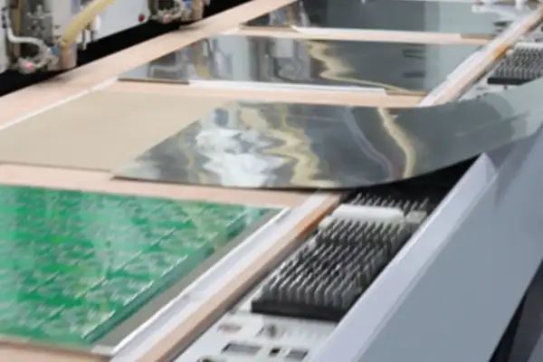
By the way, I also want to mention the importance of manufacturing process. No matter how good the design is, it must be able to be manufactured. Especially when it comes to Heavy copper and multi-layer boards.
If the factory’s process control is not strict, the lamination is not good or the hole copper is uneven, no matter how good the design is, it will be in vain.
It is often these most basic and inconspicuous links that ultimately determine product quality.
I have always felt that many people have misunderstandings about the PCB board in the charging pile. They always think that as long as the material is thick and can carry electricity, it will be fine. In fact, that’s not the case at all. Take the EV Charger PCB as an example. What it fears most is not the high temperature or high current itself, but the alternation of hot and cold day after day. If you think about it, a board will be hot under the sun during the day, and then cool down and even condense at night. This kind of torment is a great test for the circuits and vias inside.
I’ve seen some early designs have problems. They may use good FR-4 base materials and high Tg materials, which theoretically have enough heat resistance. But the problem often lies in some details, such as the copper layer of the via. If the manufacturing process is not up to standard or the materials are not properly matched, micro-cracks that are invisible to the naked eye may appear after several “thermal expansions and cold contractions.” It may still work normally at first, but as time goes by, the resistance will slowly increase, eventually leading to the complete failure of a key signal or power path. This kind of failure is very subtle and deceptive. It does not happen instantly like burning.
So now many reliable designs will emphasize this point. They not only pay attention to whether the Tg value of the material is high enough, but also pay attention to the performance of the entire board under extreme temperature cycles. This is not just as simple as choosing a “high temperature resistant” PCB, it involves every aspect from the material formula, lamination process to post-drilling processing. For example, in order to carry greater current and improve heat dissipation capabilities, many designs will adopt the Heavy copper PCB solution, which means increasing copper thickness on critical current paths. But this brings new challenges – a thicker copper layer means that when the temperature changes, the difference in expansion coefficient between it and the surrounding insulation material will be more obvious.
When it comes to reliability in wet environments, this is another problem that is easily underestimated. Many people think that applying conformal paint can solve everything, but in fact it is just the first line of defense. In a truly harsh humidity environment, water vapor is pervasive. If the PCB board itself does not absorb water well, or if there are tiny gaps that are not properly treated during lamination, water vapor will slowly seep in and stay inside. At this time, coupled with the effect of the electric field, it becomes troublesome.
I’ve heard that some high-end products undergo very stringent moisture-proof tests, simulating multiple days of extreme high-humidity environments for verification. The consideration behind this is a phenomenon called CAF – simply put, the long-term action of moisture and electric field may cause copper ions to quietly “crawl” between the glass fibers inside the board, eventually forming an invisible short-circuit channel. This process may take several months or even a year or two to show up.
So you see, designing a reliable charging pile PCB for electric vehicles is really not just about soldering a few high-power devices on. It is more like making a precise balance: it must not only ensure stability and low loss when large currents pass through (which is related to charging speed and efficiency), but also ensure that it can work stably for several years without any glitches in complex outdoor environments exposed to wind, sun, cold, winter and heat.
This requires engineers to have a very deep understanding of material properties, processing techniques, and actual application environments. Sometimes, in order to meet a seemingly simple “reliable charging” requirement, there may be a complex set of comprehensive applications of materials science and engineering design behind it.
I recently chatted with some friends who were working on electric vehicle-related projects, and found that they were all troubled by a seemingly simple thing: the circuit board that charges the car. This is not an ordinary PCB board like that in your home router. It has to withstand repeated impacts of large currents. Many people think that just thickening the copper foil is enough, right? It’s not that simple.
I have seen some early designs of EV Charger PCBs. In order to pursue high power density, the circuits were designed to be very compact. The result? When a large current is applied, local heating becomes serious. Later, everyone slowly realized the problem – you have to leave enough “channels” for the current, which cannot be solved by simply stacking thick copper. Many reliable designs now use a process called Heavy copper PCB to handle high current path parts.
Speaking of this Heavy copper PCB technology is quite interesting. It is not like ordinary circuit boards that only have a thin layer of copper foil covering the surface; instead, a special process is used to make the thickness of the copper layer in some key areas several times or even ten times that of the conventional circuit board! After this treatment, those parts that carry large currents become very solid.
But thick copper alone is not enough! You have to consider how the entire system can dissipate heat? After all, there will always be losses and heat generated during the conversion of so much energy! So now good designs will clearly plan the heat dissipation path – from the chip to the PCB to the casing and even the external environment must be taken into consideration!
I still remember a friend whose company had suffered losses due to this problem before! They designed a beautiful-looking charging module, but when they tested it, they found that the temperature rise was too high and it couldn’t work for a long time! It was later discovered that there was a problem with the design of the heat conduction path inside the PCB – even though thick copper was used, the heat was still accumulated in certain areas and could not escape!
Now the industry is paying more and more attention to this issue, especially after the automotive industry quality management system such as IATF is introduced into the field of charging equipment manufacturing, everyone’s requirements for reliability are much higher than before! In the past, you may have thought that it was enough to be powered on, but that is no longer possible now. You have to ensure that it can work stably for more than ten years in various environments!
I think this is actually a good thing and shows that the entire industry is maturing! After all, no one wants the electric car they bought to break down halfway due to charging problems, right? So companies making this product now have to seriously think about how to make their products more reliable and durable!
In fact, from the user’s point of view, we don’t care at all how advanced technology or complex processes you use. We only care about one thing: can the gun be charged smoothly after being plugged in? Does it charge quickly? Is it safe? It’s that simple! But there is a lot of work that needs to be done to achieve this simple goal!
I sometimes wonder why mobile phone chargers were so easy to break in the past but now the charging equipment for electric vehicles is so demanding? Maybe it’s because cars are related to personal safety! Problems in any link may bring serious consequences, so the standards must be set high!
Many companies are now studying how to make the charging process smarter and more efficient, but all smart functions must be based on a reliable circuit board! If you can’t even do the most basic current carrying and heat dissipation, no matter how many smart functions you try, it’s all in vain!
So to make this product, you really need to calm down and study the basic principles, and you can’t just pursue beautiful surface parameters! You have to truly understand how current flows and how heat is transferred before you can design a product that is both efficient and reliable!
I have always felt that many people’s understanding of electric vehicle charging is too superficial. Everyone only cares about whether charging is fast or not, which is inconvenient. But few people think about what is connected behind the plug and hidden inside the charging pile – the circuit board that carries huge current, which is the EV Charger PCB. It is the key to determine whether your charging experience is smooth and even safe.
I have seen some manufacturers making a fuss about PCB in order to pursue low cost. The thickness of the copper foil they used may barely meet the standards. But you know what? When large currents continue to pass through, “barely” is definitely not enough. It’s like letting fifty people walk on a small bridge in your home that can only accommodate ten people at once. Sooner or later, problems will occur.
Therefore, I was particularly happy when I saw that the industry began to emphasize the application of Heavy copper PCB. It’s not just as simple as thickening the copper a little bit. Behind it is the upgrade of the entire design idea and production process. You have to consider how to maintain stable heat dissipation under high current density and how to ensure that the connections between each layer of circuits are strong enough.
An actual case I have come across is very representative. A friend’s company makes DC fast charging stations, but the initial prototype test was always unstable. After a long investigation, I found that it was a PCB problem. The ordinary process board they originally used to keep up with the schedule and control costs found that the temperature rose too high in high-power continuous charging scenarios, resulting in severe performance degradation.
Later, they switched to a supplier specializing in thick copper plates, and the situation was completely different.
The current-carrying capacity of that kind of board has been significantly improved, and the stability of the entire charging process has also improved. This made me realize a truth: In an era of pursuing fast pace, some basic things require us to slow down and polish them.
The quality of PCB is directly related to the life cycle and maintenance cost of the entire charging pile.
Although the initial investment of a well-designed thick copper plate will be higher, it can greatly reduce the subsequent failure rate caused by overheating, short circuit and other problems.
In the long run this is more economical. I think many consumers are beginning to realize this now. They no longer just look at the price, but also care about whether the core components of the product are reliable.
This is actually a good driving force for the entire industry.
When the market begins to force manufacturers to pay attention to these intrinsic qualities, more and more truly good products will appear.
I recently discovered an interesting phenomenon when chatting with some friends who make charging piles: many people think that the problem of high current can be solved by thickening the copper foil on the PCB. This idea sounds reasonable, right? After all, larger current requires thicker “wires”. But the reality is often more complicated than that.
Take the EV Charger PCB as an example. I have seen a project that used ordinary processes to process thick copper plates in the early stage of pursuing low cost, but it suffered a big failure. They thought that everything would be fine if they used 3oz copper foil, but they ignored the details during the lamination process. Later, it was discovered that those seemingly solid traces actually developed tiny delaminations under the continuous impact of large currents, which turned into fatal faults over time. Specifically, when laminating multi-layer boards, the matching of resin fluidity and copper foil is crucial. If preheating is insufficient or the pressure is uneven, it is easy to leave hidden dangers between the copper and the substrate. These microscopic defects will gradually expand under the continuous electrothermal stress of DC or high pulse current.
This reminds me of another example regarding the integrated design of liquid cooling systems. Nowadays, many high-end charging piles are moving in this direction, but it is not just about installing cooling ducts. The real difficulty lies in how to effectively coordinate the heat distribution of the PCB with the liquid cooling channel. Some designs only mechanically add heat sinks but ignore the hot spots generated by the current path. As a result, the cooling effect is greatly reduced and unnecessary volume and weight are added. For example, if the geometry of the copper layer below the power module is not designed properly, heat may not be efficiently conducted to the coolant contact surface, but instead accumulate inside, causing local temperature rises far beyond expectations and accelerating device aging.
In fact, the application of thick copper PCB is far more than just increasing the thickness. It involves the adjustment of the entire manufacturing chain, from material selection to processing technology, which needs to be reconsidered. For example, ordinary parameters in the drilling process can easily produce burrs on thick copper plates, affecting the subsequent plating quality and threatening long-term reliability. In addition, the uniformity of electroplated copper is also a major challenge. If the copper thickness of the hole wall is inconsistent, it may cause uneven current distribution during high-frequency or large-current switching, resulting in additional hot spots and electromagnetic interference.
I increasingly feel that good charging pile design is more like a balancing problem. You can’t just focus on a certain indicator, such as simply pursuing higher current carrying capacity or cooler cooling technology, but you should pay attention to how the various parts work together. For example, thermal design needs to be carried out simultaneously with electromagnetic compatibility (EMC) design, because the shape and position of the heat sink can affect parasitic parameters, thereby changing the switching noise and radiation characteristics of the circuit.
Sometimes the most reliable solutions are not necessarily the most technologically advanced, but rather those combinations that have been fully proven to work stably. For example, in some cost-sensitive applications, the overall performance of an optimized 2oz copper foil with reasonable layout and heat dissipation design may be better than a hastily launched 4oz thick copper solution, because the latter may bring new problems in impedance matching and process reliability.
Another point that is easily overlooked is environmental adaptability. Temperature, humidity and even power grid fluctuations in different regions will pose different challenges to the core components of charging piles, which places higher requirements on the material stability and process consistency of PCBs. For example, in areas with large temperature differences between day and night, small differences in the coefficient of thermal expansion (CTE) between the PCB substrate and the copper foil will accumulate stress due to frequent thermal cycles, which may eventually lead to solder joint cracking or plated through hole (PTH) fracture.
I have seen some export products that perform well in domestic tests but have frequent problems in actual use environments. This is largely because the early stage verification is not sufficient and not enough variables are taken into account. For example, the high salt spray environment in some coastal areas can accelerate corrosion at the interface between external connectors and PCBs, and this failure mode is difficult to fully reproduce in routine tests in temperature-controlled laboratories.
After all, the core of making such power electronic products is the ability to control details. Those seemingly small process differences will often amplify into significant quality differences in long-term operation, and this is precisely the key to distinguishing excellence from mediocrity. For example, the thickness and coverage uniformity of the solder mask not only affect the appearance, but also affect the stability of the high-voltage creepage distance, which is crucial in humid environments.
I think future competition will focus more on how to make every link solid enough through systematic thinking rather than blindly pursuing a single technical parameter. After all, what users ultimately need is a safe, reliable and durable product experience, which will never change. This means that from chip selection, topology design, PCB layout, process control to complete machine testing, a closed-loop data feedback and optimization mechanism needs to be established to continuously iterate actual field test data into the design specifications.
When many people mention the manufacturing of EV chargers, they think the key lies in the software or shell design. This is actually a big misunderstanding. My experience tells me that the core component that really determines whether a charging pile can work stably and safely is often the PCB motherboard hidden inside. This board is like the heart and nervous system of the entire device.
I have seen many projects ignore the quality requirements of PCB in the early stage of the project in order to meet the schedule or reduce costs. For example, some teams will use ordinary circuit boards to handle high-power charging tasks. The result? It is common for equipment to become overheated or even malfunction after running for a period of time. This made me realize a problem: for high-power applications, “enough” often means “not reliable enough.” Especially in the context of fast DC charging.
This has to mention a special process-thick copper PCB. This kind of board is not just about thickening the lines. It requires thicker copper layers deposited during the manufacturing process to carry large currents. Imagine that the circuit board in an ordinary household appliance may only need to handle a few amps of current, but the main circuit of a 150-kilowatt DC fast charging station may have to continuously withstand hundreds of amps of large current.
If you still use a conventional PCB, the thin copper foil will quickly become hot or even burn due to the heat generated by the resistor.
I know an engineer friend who suffered this loss.
The first-generation AC charging pile prototype developed by their team tested normally in the laboratory. But after it is installed on site, it will automatically cut off the power for several hours of continuous operation in high temperature environments in summer.
After disassembling and inspecting, it was discovered that the power trace area on the PCB had an excessive temperature rise due to continuous high current operation, triggering the thermal protection mechanism. They had to redesign the board and use a thick copper process to solve this problem. This lesson tells us directly: in the field of power electronics, compromises in hardware design will eventually cost you in some form.
Of course, having a good hardware foundation is not enough. There are now a wide variety of charging pile products on the market. How do consumers or buyers know which one is more reliable? This involves the issue of industry certification.
I think these certification marks are actually a kind of “technical credit”. For example, the familiar CCC certification is a stepping stone to enter the domestic market; and if your products want to be sold in North America, UL certification is almost necessary; in the European market, the CE mark is required. These certification processes are very rigorous.
They will not only test whether your finished products are safe and reliable, but also trace back to whether the quality management system of your entire production process is up to standard – from the source of component procurement to every soldering point on the production line will be carefully reviewed.
I remember that a start-up company once developed a wall-mounted charger with a very novel design, but because it was in a hurry to market it, it rushed into production without carefully preparing the documentation and testing procedures required for UL certification. As a result, after the products were shipped to the United States, they were all returned by the dealer because they could not provide complete certification documents, resulting in heavy losses. This incident taught me that compliance requirements should be taken into account in the early stages of product development rather than being remedied after the fact.
After all, whether you choose a thick copper PCB with stronger performance to ensure hardware reliability or invest time and effort in obtaining various international certifications, it is all about building user trust. After all, when people park hundreds of thousands of cars in front of your charging pile, they need to be sure that the device can charge the battery safely and quickly, rather than being disconnected at critical moments or even causing safety hazards.
This kind of trust is not accumulated through advertising but through solid design and strict quality control in every detail.
I used to think that the most troublesome thing about making products like charging piles is passing the certification. Different countries have various requirements, and just preparing the materials can be a headache. Later, I slowly discovered a more fundamental question: Are we too dependent on those standard documents? Those thick GB or international standards are of course important. But many times, they are just the minimum threshold for market entry. What really determines whether a product can be accepted by users and used for a long time is often something other than the standard.
I have met some of my peers who see certification as their ultimate goal. Once the product gets the certificate, everything will be fine and it can be quickly launched into the market. The result? Users will still encounter various minor problems in actual use, such as poor contact during charging, or the device is unstable in bad weather.
These details may not be specified in the standard, but they exactly affect the user experience.
My own experience is that rather than focusing all my energy on studying those complicated provisions. It is better to spend more time to understand the actual usage scenarios. For example, an EV Charger PCB board used on an outdoor charging pile needs to face more than just the constant temperature and humidity environment in the laboratory. It may experience high temperatures in summer, severe cold in winter, humidity and even salt spray. The combination of these factors is a real test for PCB.
This involves material selection and technology. Nowadays, many high-power devices use Heavy copper PCB to carry larger currents. This is indeed a valid technical direction. But thick copper also brings new challenges such as thermal design and mechanical stress issues. If you simply increase the copper thickness without considering the thermal expansion coefficient matching of the overall structure, prolonged thermal cycling may cause the solder joints to crack. These problems may not be immediately exposed in standard routine testing.
So I think when making products, you can’t just focus on ticking the boxes on the certification list. What’s more important is to establish a “scenario-based” thinking model. Ask yourself more: Where will this charging pile be installed? What will users do? What is the most likely problem area? Use these questions to design your PCB layout, select components, and even plan test plans. The products produced in this way are more resilient.
Ultimately, standards and certification are necessary regulatory frameworks. But they should not become the upper limit of our thinking or the constraints of innovation. A truly good engineer should know how to go one step further on the basis of meeting these basic requirements to solve problems that have not yet been defined but that users will actually encounter. This process will of course be more time-consuming and labor-intensive, but the value it brings is long-term.
I always believe that good products speak for themselves. When users find that your device can complete charging tasks stably and reliably in various environments, that sense of trust cannot be replaced by any certification mark. This kind of trust is the most solid moat for a brand.
Just like many of the things we use in daily life, the most comfortable and easy-to-use ones are often not the ones with the most complex functions and the most beautiful parameters, but the ones whose designers have truly considered the meticulous considerations of how you will use it under what circumstances, which is far more weighty than a certificate.
I recently chatted with some friends who make charging piles and found that everyone has different concerns when choosing a PCB supplier. Many people ask about price and delivery time when they first come up, which is certainly true, but I think this matter needs to be viewed from more dimensions. Take the EV Charger PCB as an example. It carries a lot of current and heat dissipation pressure. I have seen some boards turn yellow or even bulge near the solder joints after being used for a period of time. The problem often lies in the basic materials or process details.
So my opinion is that the concept of “thick copper” cannot just be based on the numbers on the specification sheet. This does not mean that everything will be fine after using Heavy copper PCB. You have to see how it is implemented.
Is the entire board thickened evenly, or is it only partially strengthened on key power channels and ground layers? The latter actually has higher requirements on design and craftsmanship. I prefer the latter because it allows for better control over cost and overall mechanical stress on the board while maintaining performance. Simply pursuing the use of very thick copper foil for the entire board will sometimes lead to difficulty in lamination and the risk of warping.
When it comes to testing, this may be the most easily overlooked and least deceitful aspect. Many suppliers will show you a bunch of certifications. But the certificate is the threshold, and the real effort lies in the daily verification later. I particularly value how they conduct testing at the end of the production line. In addition to conventional electrical performance continuity tests, are there additional current-carrying capacity and temperature rise spot checks for those high-current paths? Will they perform slice analysis regularly, not to show you beautiful samples, but to randomly inspect batch-produced boards to see if the copper thickness of the hole wall is really uniform and up to standard, and whether there is any potential risk of delamination in the inner layer bonding? These data reflect the true level of process control.
Think further about the system capabilities of a PCB factory. Nowadays, there is a lot of talk about smart manufacturing and traceability, which is indeed important. A good MES system can allow you to clearly know the origin of each batch of plates, the life of each tank of potion, and the parameters of each key process. But is this system actually used for process control and problem analysis, or is it just for a beautiful interface display during customer audits? These are two completely different states.
I always believe that choosing a partner, especially for a basic and critical component like PCB, depends on a comprehensive “certainty”. What you need to make sure is not just that the boards delivered this time are okay, but that the same stable level can be maintained for every delivery in the next one, two or even more years. This certainty comes from the other party’s engineering team’s depth of understanding of the principles, from their persistent control of every parameter of the production line, and from their speed and candor in solving problems when an exception does occur. Price is certainly an important consideration, but it should be something weighed only after all of these dimensions of “certainty” have been met. After all, the reliability of a PCB installed in a charging pile is directly related to the end user’s safety experience and brand reputation. This account must be calculated in the long run.
Many people think that making charging pile circuit boards is just a matter of stacking materials and thickening the copper. This idea is actually quite one-sided. I have seen many projects stuck in the supply chain. You think you can sit back and relax after specifying a certain high-standard material. However, the supplier says “out of stock” or “delivery will take eight weeks”, and the entire project schedule is completely messed up. Only then will you realize how valuable those manufacturers that can stably provide plates with special specifications are. They usually do not rely solely on factories in one region. Global production capacity layout is the real confidence.
For example, they may have cooperative factories in Southeast Asia and Eastern Europe and establish a shared raw material reserve so that when logistics or production is interrupted in one place, other resources can be quickly mobilized to make up for it, ensuring that supply continuity is not interrupted.
When it comes to thick copper plates, your first reaction may be heat dissipation and current carrying capacity. This is certainly true, but the crafting challenges it presents are often underestimated. After the copper layer is thickened, the precision control of etching and the uniformity of lamination are big problems. If it is not done well, the edges of the circuits are rough or there is copper residue, it is just a small matter, but it will seriously affect the long-term reliability of the board. This cannot be solved by just looking at the parameters. It relies heavily on the factory’s experience and technical accumulation. Some manufacturers can make very thick copper, but the yield is unstable and performance varies between batches. For example, when etching thick copper, the solution concentration, temperature and spray pressure must be precisely matched. A slight deviation will lead to excessive side etching, affecting the precise shape and current carrying capacity of the line. The lamination process requires precise control of temperature, pressure and vacuum to ensure that the resin can fully fill and firmly bond the layers to avoid delamination or cracking under high loads in the future.
The role PCB plays in the charging system is far more complex than we think. It is not just a carrier for connecting components, but more like a high-speed command center. How the current flows, how the heat dissipates, and how the signals are transmitted are all planned in the layers of circuits. Especially in high-power fast charging scenarios, the instantaneous current is very large and the impact on the board is continuous, which requires it to have both a strong physique and sharp responses. Therefore, when designing, you can’t just look at electrical performance but also consider mechanical stress and thermal management. For example, engineers need to use simulation software to pre-analyze the stress generated between materials with different thermal expansion coefficients during frequent high-current on-off cycles, and optimize layout and material selection accordingly to prevent fatigue cracking of solder joints. At the same time, the shape of the heat dissipation vias and copper foil will be carefully designed to efficiently conduct the heat from the hot spot area to the heat sink.
Nowadays, many people are talking about supply chain security. I think specifically in circuit board production, we need to reduce uncertainty. For example, whether the sources of raw materials are diverse, whether there are proven alternatives, and whether the factory’s production process is transparent and traceable. These details often determine the lower quality limit of the final product. It is difficult for a poorly managed supply chain to produce stable and reliable circuit boards. For example, a rigorous factory will conduct sampling tests on each batch of incoming copper-clad laminates, measure key indicators such as glass transition temperature, dielectric constant, and thermal expansion coefficient, and bind the data to the production batch to achieve full traceability. In this way, even if problems arise in the future, the material link can be quickly located.
I always believe that good products are both designed and manufactured. No matter how perfect you design the circuit diagram, if the factory’s production process cannot keep up, all the previous efforts may be in vain if inappropriate materials are used or improperly handled. Especially for equipment that needs to work outdoors for a long time, circuit boards have to deal with environmental factors such as moisture, temperature differences and even salt spray corrosion, which test not only the initial performance.
When choosing a partner, I look more at their track record of handling complex requirements rather than simply listening to what they promise. For example, I will examine whether they have provided circuit boards for communication base stations or offshore wind power equipment. These cases can prove the durability of their products in harsh environments and their process’s ability to control special requirements such as three-proof coating and thick copper processing.
Ultimately, the industry is shifting from the pursuit of parameters to the pursuit of comprehensive experience. Stability and durability will become more important competition dimensions. A good circuit board should work in obscurity for many years rather than just a few beautiful numbers on the parameter sheet. This means that every aspect from material selection, structural design to manufacturing process needs to be optimized with long-term reliable operation as the core goal to ensure that it is still solid and reliable where users cannot see it.
When we talk about 5G, we often only focus on the grand
In the BLDC motor controller project, we are often attracted by the
From the production dilemmas of irregularly shaped boards to practical observations on
- 중소규모 배치 생산 전문가
- 고정밀 PCB 제작 및 자동화된 조립
- OEM/ODM 전자 프로젝트를 위한 신뢰할 수 있는 파트너
영업 시간: (월~토) 9:00~18:30