
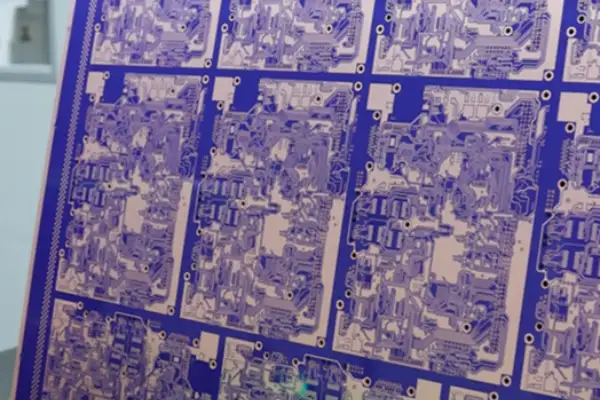
Battery Monitoring System PCB: Why the Hardware Foundation Determines Everything Else
BMS reliability isn’t decided by algorithms — it’s decided by the PCB
I have long felt that many people’s understanding of RF circuits is somewhat misguided. People tend to fixate on chip and antenna designs, as if these were the sole decisive components. However, across the various projects I have managed, I’ve discovered that what truly determines whether a high-frequency system operates stably is often that unassuming circuit board right beneath your feet.
Take, for instance, a millimeter-wave radar front-end module project I worked on previously. Initially, we utilized a standard high-frequency organic substrate, and the test data appeared satisfactory. Yet, the moment the ambient temperature shifted by just a few degrees—or after the system had been operating continuously for a period—the entire system’s noise figure would begin to fluctuate erratically. We spent weeks tweaking the matching networks and swapping in more expensive amplifier chips, but the results remained unsatisfactory. Eventually, we pinpointed the substrate as the source of the problem; we decided to switch to a ceramic PCB material specifically designed for RF applications, and the situation changed instantly.
It felt akin to giving the entire system a more stable foundation. The signal’s phase stability improved dramatically; the minute frequency shifts previously caused by temperature drift became virtually imperceptible. More importantly, its thermal dissipation capability was on a completely different level. The temperature distribution around the high-power components became far more uniform—a factor that directly elevated the entire module’s long-term reliability to a new standard. Many people may not realize this: in the realm of RF engineering, thermal management is, in essence, an electrical problem.
I have seen far too many engineers pour vast amounts of energy into design simulations while neglecting the inherent limitations imposed by the materials themselves. They often operate under the assumption that as long as their simulation models are sufficiently accurate, the circuit will perform exactly as intended. However, the reality is that once your operating frequency enters the high-frequency—or even millimeter-wave—range, the intrinsic properties of the material itself—such as the temperature stability of its dielectric constant and its dielectric loss tangent—become direct participants in the electromagnetic field propagation process, evolving into an indispensable element within your circuit equations. At this stage, ordinary organic substrates resemble a somewhat unstable stage: the actors are performing upon it, yet the stage itself is subtly swaying beneath their feet.
Consequently, my stance regarding ceramic substrates is now unequivocal: they are not merely a “high-end alternative,” but rather the inevitable choice when operating within specific performance boundaries. When your requirements demand extremely low loss, exceptionally high thermal conductivity, and a platform that remains highly impervious to environmental fluctuations—this is the definitive solution. Admittedly, the associated costs are higher, and the manufacturing processes are more complex; this necessitates a careful trade-off analysis during the initial stages of design.
Nevertheless, my contention remains that if your objective is to achieve peak performance and absolute reliability, such an investment is entirely justified. This is because it addresses fundamental physical limitations at their root, rather than attempting to compensate for material deficiencies through the implementation of overly complex circuitry.
I have long felt that many people harbor certain misconceptions regarding material selection within the realm of RF design. The moment “high performance” is mentioned, people’s minds immediately jump to expensive, imported specialty materials or convoluted processing schemes. In reality, however, it is often the most fundamental elements that end up being overlooked.
Take, for instance, a project I recently participated in. We were designing a miniaturized transceiver module for satellite communication when we encountered a critical thermal dissipation bottleneck. Several members of the team proposed implementing a liquid cooling system or experimenting with solutions involving graphene coatings. I, however, insisted that we first attempt the most traditional approach: utilizing a ceramic substrate.
And the result? You guessed it: the problem was solved just like that.
What many people may not realize is that ceramic, as a material, possesses numerous inherent advantages. Unlike certain polymer-based materials, it does not exhibit a high degree of sensitivity to temperature fluctuations. I recall an instance where we subjected an alumina-based sample to a rigorous thermal cycling test, oscillating its temperature between -40°C and +120°C dozens of times. Upon completion of the testing, we discovered that its dielectric properties remained virtually unchanged.
This experience reminded me of an earlier filter design project I worked on using standard epoxy-resin PCBs. At the time, the product passed all factory acceptance tests without issue; however, after being deployed at the client’s site for a few months, the operating frequency drifted so drastically that the device became completely non-functional.
Subsequent analysis revealed that the issue stemmed from environmental temperature fluctuations causing the PCB substrate to undergo cycles of expansion and contraction, thereby altering its electromagnetic characteristics. Since that incident, I have placed a particularly strong emphasis on material stability in all my designs. When it comes to thermal management capabilities, I believe this is one of the most underestimated aspects of ceramics.
Nowadays, many RF power devices are required to handle hundreds of watts of heat; if the heat dissipation cannot keep up, then concepts like linearity and efficiency become entirely moot.
I have seen far too many examples of designs where performance was compromised due to thermal issues.
On one occasion, we tested a power amplifier module intended for use in base stations. We employed the exact same circuit design but fabricated it on two different substrates for comparison: a standard FR4 board and an aluminum nitride (AlN) board. The results showed a temperature difference of 30 to 40 degrees Celsius—a disparity that directly impacted the stability of the output power.
Furthermore, I’ve noticed a common misconception among many people: they assume that superior thermal conductivity inevitably implies higher costs. In reality, many domestically produced aluminum nitride substrates available today are of excellent quality, and their prices have dropped significantly. They serve as perfectly viable replacements for many of those overly elaborate, “fancy” solutions.
As for the issue of integration density, I observe a prevailing trend where everyone strives to miniaturize everything; however, this pursuit sometimes comes at the expense of reliability.
Low-Temperature Co-fired Ceramic (LTCC) technology certainly enables the creation of more compact passive components, but I would argue that not every application requires such high integration density. Particularly in high-power scenarios, an appropriate spatial distribution of components can actually be beneficial for both heat dissipation and isolation design.
I have encountered designers who, in their quest for miniaturization, crammed all their inductors and capacitors into a multilayer structure—only to find that the resulting severe thermal coupling significantly degraded the overall performance.
Therefore, my stance is that when selecting materials, one cannot simply look at technical specifications in isolation; one must also take the specific application scenario into account.
For instance, in the case of military or aerospace equipment—which demands long-term operational stability—reliability may well be a more critical factor than shaving off a few millimeters in size. Conversely, for consumer electronics, cost-effectiveness and integration density are likely the primary considerations.
Ultimately, no single material is a universal panacea. However, I firmly believe that in many RF applications, the comprehensive performance of ceramic substrates warrants far greater attention. Especially in scenarios where stability and thermal management are paramount, ceramics often provide a simple yet effective solution—without the need to wrestle with complex, cutting-edge technologies or fabrication processes. Sometimes, the simplest approach is indeed the most reliable one—a truth I have come to deeply appreciate throughout my many years of design work.
I’ve long felt that many people’s understanding of RF circuits is somewhat skewed; they tend to assume that the circuit design itself is the entirety of the challenge. In reality, you could spend months fine-tuning a layout to absolute perfection, yet if you place it inside a mediocre package, its high-frequency performance could plummet instantly. It’s a bit like meticulously engineering a high-performance sports car engine, only to mount it on a set of cheap, low-grade tires. My introduction to ceramic substrates was quite straightforward: at the time, a specific project I was working on utilized standard PCB materials, but we consistently encountered instability within a particular frequency band. Later, we decided to experiment by switching to ceramic-based boards for the RF section; almost immediately, those inexplicable signal attenuation issues diminished significantly. Ceramic substrates—particularly Low-Temperature Co-fired Ceramics (LTCC)—possess a surface roughness far lower than that of conventional FR-4 materials. This characteristic directly reduces conductor losses as well as losses caused by the skin effect on the surface of transmission lines. Furthermore, the exceptional stability of their dielectric constant ensures that critical parameters—such as resonant frequencies—do not drift in response to environmental fluctuations; this is absolutely vital for frequency-sensitive circuits like filters and oscillators.
Ceramics truly possess unique advantages within the realm of RF engineering. Unlike certain organic PCB materials, their electrical characteristics do not readily shift in response to changes in temperature or humidity—a stability that is paramount for applications requiring consistent frequency performance. Moreover, ceramics exhibit superior thermal conductivity—a subtle yet significant advantage for RF chips that generate substantial heat. For instance, consider a power amplifier chip with a 10-watt output: if the heat it generates is not dissipated promptly, the chip’s junction temperature will skyrocket. This rapid temperature rise can lead to gain compression, reduced efficiency, and even permanent device failure. The exceptional thermal conductivity of a ceramic substrate acts like a high-efficiency highway, rapidly channeling heat away from the chip and transferring it to the device’s housing or heat sink.
When it comes to the packaging stage, many engineers tend to view it merely as the final “wrapping” step; however, in the high-frequency domain, the package itself is an integral part of the circuit. The package’s pins, lead frames, and even its internal air cavities can all introduce parasitic inductance and capacitance. These parasitic parameters interact with the chip’s input and output impedances, thereby altering its impedance matching characteristics. In the millimeter-wave frequency band, a lead wire just a few millimeters in length can effectively act as a significant inductive component—potentially completely undermining the carefully engineered performance of the chip.
I have observed engineers who densely populate their boards with discrete components, under the assumption that doing so enables them to cram in more functionality. However, at high frequencies, this approach introduces a multitude of unpredictable solder joints and unnecessary interconnection paths, ultimately making the maintenance of signal integrity far more difficult to control. Every solder joint represents a potential impedance discontinuity that can reflect signals; conversely, excessively long interconnect traces act like antennas—capable of both radiating energy (thereby causing loss) and picking up external interference.
It is no coincidence that many manufacturers are now opting to integrate the entire RF front-end into a single, complete ceramic-packaged module. This approach allows for shorter and more direct signal paths. This “System-in-Package” (SiP) technology integrates multiple bare dies—such as power amplifiers, low-noise amplifiers, switches, and even filters—within a single ceramic cavity. By utilizing precise thin-film or thick-film processes to establish interconnections directly within the substrate, this method virtually eliminates the parasitic effects and uncertainties typically associated with traditional PCB-level interconnections.
Another advantage of ceramic packaging is that it facilitates superior ground continuity. High-frequency signals demand a high degree of integrity in the ground plane; a discontinuous ground reference can severely degrade the performance of the entire system. Ceramic packages typically feature a fully metallized base layer that enables a large-area, low-impedance ground connection to the main system board. This provides a “solid” ground potential reference for all internal circuitry—a critical factor for suppressing common-mode noise and ensuring smooth signal return paths.
Of course, there are significant variations among different ceramic materials. Beyond core parameters such as dielectric constant, loss tangent, and thermal conductivity, these materials also differ in terms of mechanical strength, processing precision, and compatibility with metal pastes during co-firing. For instance, in high-density interconnect designs requiring numerous micro-vias, factors such as the material’s drillability and the reliability of the via-wall metallization become essential considerations.
Alumina (aluminum oxide) remains the most widely adopted industrial choice; it offers excellent cost-effectiveness and utilizes mature processing technologies, making it more than adequate for a great many standard RF applications. However, if your objective is to achieve extreme performance or handle high-power signals, aluminum nitride may be a more compelling option to consider, as it boasts significantly superior thermal dissipation capabilities. Furthermore, the coefficient of thermal expansion (CTE) of aluminum nitride closely matches that of silicon semiconductor chips; this significantly mitigates the thermomechanical stress induced by thermal cycling, thereby enhancing the long-term reliability of the package in harsh operating environments.
Ultimately, the choice of ceramic substrate depends entirely on your specific requirements. If you are simply designing a standard wireless communication module, there is no need to blindly pursue the most expensive material available. However, if your design operates at high power levels or within high-frequency bands, the intrinsic properties of the materials themselves become one of the critical factors determining success or failure. For instance, in 77 GHz automotive radar systems or 5G millimeter-wave base stations, even minute variations in the substrate material’s loss tangent—when accumulated across long transmission lines—can lead to a significant degradation in system sensitivity or transmission efficiency.
I believe that RF design should be approached from a more holistic, systems-level perspective. From the chip to the circuit board and finally to the packaging, every single stage influences the ultimate performance outcome. It is akin to a chain, where the overall strength is determined by its weakest link. An exceptional RF engineer must simultaneously act as a materials scientist, a thermal management expert, and a structural designer, requiring them to comprehensively consider the synergistic design of electrical, thermal, and mechanical aspects.
Occasionally, investing a little extra cost upfront in materials and packaging can actually spare you a great deal of trouble during the subsequent debugging and fine-tuning phases. By selecting high-quality ceramic substrates with ample performance margins—along with advanced packaging solutions—during the project’s inception, you can preemptively avoid mass production issues or customer complaints stemming from inadequate environmental robustness or inconsistent product quality. When viewed through the lens of total lifecycle cost, this often proves to be the more economically sound choice.
I have long felt that many people’s understanding of ceramic circuit boards is somewhat misguided. Whenever the topic arises, people invariably tend to emphasize the impressive—and sometimes intimidating—numerical specifications, such as thermal conductivity ratings or ultra-low loss figures. While it is certainly true that these metrics are important, I have always felt that material selection—particularly in application scenarios like RF ceramic PCBs—is less about simply chasing a “performance champion” and more about finding a suitable partner. You must assess whether the material is truly compatible with the specific chips you are utilizing, your manufacturing processes, and even your projected production scale.
Take, for instance, the highly popular “co-firing” process—whether low-temperature (LTCC) or high-temperature (HTCC). Many people assume this technology exists solely to enable the creation of smaller and thinner circuits. While that is indeed true, its deeper value lies in the fact that it allows the material and the circuitry to “grow together” as a single, unified entity. Consider the traditional approach: a finished circuit board is “assembled” together with external components, inevitably creating various interfaces and connection points between them. The co-firing process, however, operates differently; while the ceramic material is still in its “green tape” (unfired) state, conductive traces and passive components—such as capacitors and inductors—are embedded directly within it, and the entire assembly is then fired and formed in a single, monolithic step. This is akin to constructing a building: instead of erecting the walls first and then retrofitting the plumbing and electrical wiring, you design the conduits directly into the structural framework from the very outset, casting them together as a single unit. The result is a product with an internal structure that is seamlessly integrated—a design where “ppm-level” dimensional stability truly holds significance.
Why is this the case? Because RF signals are particularly “delicate,” exhibiting extreme sensitivity to even the slightest variations along their transmission path. If the coefficient of thermal expansion (CTE) of your substrate material does not match that of the chip mounted upon it—for instance, if one is around 4 ppm/°C while the other differs significantly—then any fluctuation in temperature will cause the two components to expand or contract at disparate rates. This disparity generates mechanical stress, which, over time, can lead to cracked solder joints or performance drift. Conversely, a ceramic substrate produced via “co-firing” involves the simultaneous sintering of its various layers; they bond tightly into a cohesive whole right from the start. Consequently, the substrate’s overall CTE is uniform and controllable, allowing for a much better thermal match with the semiconductor chip. This approach is far more reliable than simply attempting to force a fit using a standalone sheet of high-performance—yet thermally “incompatible”—material. For example, in the millimeter-wave frequency band, a deformation of just a few microns can trigger impedance mismatches and signal reflections; an integrally formed structure, however, drastically mitigates such risks.
I have encountered cases where, in the pursuit of ultimate thermal conductivity, designers selected a specific type of expensive, specialized ceramic—only to overlook its compatibility with their subsequent packaging processes. This oversight resulted in abysmal yield rates and, ironically, skyrocketing costs. Sometimes, taking a step back to choose a more balanced—yet technologically mature—material—such as standard alumina ceramic with superior CTE matching—can prove more advantageous. By coupling this choice with an optimized multi-layer routing design, the final product often achieves superior stability and cost-effectiveness. For instance, in the power amplifier modules of 5G base stations, designers have successfully leveraged mature Low Temperature Co-fired Ceramic (LTCC) technology to achieve high-density integration and consistent batch production, all while simultaneously ensuring effective heat dissipation and signal integrity.
Therefore, my view is that you shouldn’t let yourself be led astray by flashy, exaggerated specifications. First, clearly define the actual operating environment for your product—specifically, what are the true constraints regarding size, weight, reliability, and cost? Only then should you look for the type of ceramic substrate—including its manufacturing process (such as whether co-firing technology is utilized)—that best aligns with your overall requirements. This process is akin to having a suit custom-tailored rather than rushing into a store to grab the most expensive garment on the rack; a proper fit is always the top priority. For instance, automotive radar systems must withstand thermal cycling ranging from -40°C to 125°C; this demands that the substrate material, the chip, and the packaging enclosure all “dance in harmony” across this entire temperature spectrum.
After all, even the finest material remains nothing more than a laboratory curiosity if it cannot be stably integrated into your production ecosystem. True engineering wisdom often lies in striking a balance and making trade-offs, rather than blindly fetishizing a single performance metric. This principle is particularly evident in RF design, where there are no isolated “heroes,” but rather collaborative systems in which every single link in the chain must function with absolute precision. It is much like a musical ensemble: while the absolute pitch of each individual musician is undoubtedly important, it is their mutual coordination and resonance that ultimately create a beautiful piece of music.
Whenever I see someone speak in such absolute terms regarding the selection of ceramic substrates, I find it somewhat amusing. They make it sound as if choosing a material were as simple as ordering a meal—merely ticking off items on a menu. In reality, nothing could be further from the truth; you must first clearly define exactly what it is you are attempting to build.
I have encountered far too many people who, right off the bat, ask: “Is aluminum nitride the absolute best choice?” This question, in itself, is essentially meaningless. It is akin to asking: “Is a sports car the best vehicle?” The answer depends entirely on whether you intend to drive to the grocery store or hit the racetrack. In the realm of RF circuit design, there is no such thing as a universal panacea—only solutions that are either suitable or unsuitable for the specific application.
Take aluminum oxide, for example: many people assume that because it is inexpensive, its performance must be inferior—a notion that is pure prejudice. I once managed a filter project for a 5G base station client who initially insisted on using aluminum nitride, operating under the assumption that a higher price tag automatically equated to superior quality. However, after conducting a thorough analysis, we discovered that the operating frequency of their specific module was not actually that high; what they did require, however, was exceptionally high surface flatness and robust metallization adhesion. We ultimately opted for a high-purity aluminum oxide substrate treated with a specialized process; not only did it meet every performance benchmark, but it also slashed production costs significantly—a result that even the client themselves had not anticipated.
Speaking of manufacturing processes, I believe many people today harbor a common misconception: an excessive, almost obsessive pursuit of “advanced” technologies. LTCC certainly sounds impressive—it enables multi-layer 3D integration—but its long design cycles and high tooling costs can be a burden for small-batch R&D projects. Sometimes, a simpler thick-film printing process offers greater flexibility; you can finalize your design layout today and have samples ready for testing and iteration by tomorrow.
The intrinsic properties of ceramic materials are also quite fascinating. People often focus solely on thermal conductivity figures while overlooking the critical issue of thermal expansion matching in real-world applications. If you solder a high-thermal-conductivity chip onto a substrate, and the coefficients of thermal expansion for the two materials differ significantly, temperature fluctuations can induce mechanical stress. Over time, this can compromise the system’s long-term reliability. Therefore, material selection should never be based on a single metric alone.
I particularly enjoy examining ceramic substrates produced by different manufacturers—even those utilizing identical alumina formulations—because subtle variations in the sintering process can result in distinct differences in the final dielectric constant and loss tangent values. These minute details—which rarely appear on standard datasheets—often determine whether or not your RF circuit will ultimately function stably.
With many modern designs shifting toward higher frequency bands—such as those found in Wi-Fi 6E or millimeter-wave radar applications—substrate surface roughness has become a critically important factor. A rough surface increases conductor losses and degrades signal integrity. Some manufacturers offer surface polishing options; while this may add slightly to the cost, it is a worthwhile investment for certain high-frequency applications.
Ultimately, selecting a ceramic substrate requires a holistic approach. You must carefully balance factors such as performance requirements, budgetary constraints, production lead times, and long-term reliability. Don’t be intimidated by high-sounding technical jargon; instead, consult with experienced engineers—sometimes, the simplest solution turns out to be the most effective one.
Lately, I’ve been delving into some of the most vexing challenges in RF circuit design—particularly as operating frequencies continue to climb. You quickly discover that many materials previously considered “adequate” suddenly become completely unsuitable. Take standard FR4 substrates, for instance: while they perform acceptably at lower frequencies, once you venture into the high-frequency or millimeter-wave bands, the resulting signal loss becomes alarmingly high. This type of signal loss stems primarily from the fact that the dielectric loss factor (Df) of the substrate material degrades significantly as frequency increases; concurrently, the skin effect—exacerbated by conductor surface roughness—intensifies, causing a substantial portion of signal energy to be converted into heat. This severely compromises transmission distance and signal-to-noise ratio.
Consequently, turning one’s attention to ceramic materials becomes a natural progression. Many people, upon hearing the term “ceramic substrate,” assume its sole purpose is to dissipate heat from high-power devices; in reality, however, the role it plays in the RF domain extends far beyond that. Its stable dielectric constant and exceptionally low loss characteristics are absolutely critical for maintaining signal integrity. I have witnessed numerous projects where, in the initial stages, standard materials were selected to cut costs—only for the project teams to find themselves scrambling later on, struggling desperately to mitigate the resulting signal loss issues. For instance, in the case of a phased-array antenna prototype operating at 28 GHz, switching the substrate material from FR4 to alumina ceramic could potentially reduce insertion loss by more than half—a factor that directly determines whether the system’s sensitivity and effective radiated power can meet the required specifications.
Turning to specific manufacturing process routes, I find the DPC (Direct Plated Copper) method particularly intriguing. It adopts a highly refined approach, akin to that of semiconductor fabrication. The process begins by applying an extremely thin “seed layer” onto a smooth ceramic substrate using vacuum deposition. Subsequently, photolithography (exposure) and electroplating techniques are employed to define and construct the circuit traces. The entire procedure sounds inherently precise—and indeed, its primary advantage lies in its ability to produce exceptionally fine circuit patterns with line widths measured in microns. For RF microsystems requiring ultra-high integration density, this capability represents virtually the only viable option. This level of precision makes it possible to integrate filters, couplers, and even antennas within a minuscule footprint, establishing DPC as one of the key enabling technologies for System-in-Package (SiP) solutions.
Of course, its drawbacks are equally apparent: it is both expensive and slow to manufacture. The vacuum deposition equipment itself carries a hefty price tag, and the overall process is far more complex than traditional methods; consequently, the cost per individual substrate board skyrockets. This inherent cost structure effectively precludes its use in mass-market consumer electronics. Beyond equipment depreciation, factors such as high-purity sputtering targets, stringent environmental controls, and complex yield management protocols all contribute to driving up the final cost, resulting in a unit price for DPC-based substrates that can be tens of times higher than that of substrates produced via traditional thick-film or HTCC processes. Consequently, you often face a very practical trade-off: is it truly worth incurring exorbitant costs just to achieve that last ounce of extreme performance? In scenarios with exceptionally stringent requirements regarding size and precision—such as certain military T/R modules or cutting-edge millimeter-wave modules—you have no choice; you must employ processes like DPC. However, in the vast majority of commercial applications, you might take a step back to explore potential compromise solutions. For instance, for certain sub-6GHz base station filters, utilizing Low Temperature Co-fired Ceramic (LTCC) technology might strike an excellent balance between performance and cost. Although its circuit precision is slightly inferior, it enables multi-layer 3D integration, thereby achieving comparable space-saving benefits.
In my own experience, selecting a specific substrate and manufacturing process is never merely a technical matter; it is more akin to the art of walking a tightrope between performance, reliability, and cost. You cannot simply fixate on the impressive data generated in a laboratory setting; you must also consider whether the product can be mass-produced and, crucially, whether customers are willing to pay a premium for that marginal performance boost. Factors such as a material’s long-term thermal reliability, its Coefficient of Thermal Expansion (CTE) match with the semiconductor chip, and the stability of its supply chain often present challenges during the mass production phase that are far more intractable than the initial electrical performance specifications.
Ceramic materials still hold a vast, untapped potential within the RF domain. As communication frequencies continue to push into higher bands—such as the upcoming 6G era—the demands for low signal loss and high stability will only become more exacting. This trend may, in turn, drive down the costs of processes like DPC and accelerate their widespread adoption—who knows? The pace of change in this industry is invariably faster than we anticipate. The exploration of new materials also continues apace; for instance, the exceptional combination of thermal dissipation and RF performance offered by Aluminum Nitride, or the development of advanced composite material systems, could well prove to be “game changers” in the future, providing engineers with a more diverse array of options.
I have long felt that many people harbor misconceptions regarding the application of ceramic substrates in the RF field. People tend to constantly emphasize their high-performance parameters or technical advantages. In my view, however, the true value of these materials lies in their ability to resolve the vexing, real-world engineering problems that plague practical design and implementation.
Take millimeter-wave applications, for example. In the past, when designing for high-frequency bands, our greatest fear was the instability and complications caused by the materials themselves. Conventional PCB substrates are simply too susceptible to temperature fluctuations. You could spend countless hours painstakingly tuning a circuit, only to find its performance drifting wildly once the summer heat set in—and then behaving completely differently again come winter. This kind of uncertainty is an absolute nightmare for engineers.
The true strength of ceramic substrates lies in their stability. It’s not just about their low loss or excellent dielectric constants—though those are certainly impressive—but rather the fact that you can achieve predictable results across a wide range of operating environments.
I encountered a fascinating example of this in the context of automotive radar applications. As you know, many modern vehicles are shifting toward higher frequency bands—77 GHz, and even 81 GHz, are becoming increasingly common. At these frequencies, even the slightest microscopic variation in the circuit board material can have its effects significantly amplified.
During one testing phase, we discovered that an identical circuit design performed wildly differently depending on the specific batch of standard PCB material used. Some batches delivered excellent performance, while others fell short. However, once we switched to a ceramic substrate, the problem vanished completely.
This wasn’t because the raw performance metrics saw a massive boost, but rather because the material characteristics remained remarkably consistent from one batch to the next. That level of consistency is absolutely critical for mass production.
Another point I feel is rarely discussed is the increased design freedom that ceramic substrates afford engineers.
Thanks to their inherent stability, you can boldly experiment with circuit topologies that you might have previously considered too risky to implement.
For instance, within complex impedance-matching networks, you can pack components much more densely without having to worry about temperature fluctuations causing critical parameters to drift out of spec.
This kind of design flexibility can, at times, be far more valuable than simply shaving a few decibels off the signal loss.
Of course, ceramic substrates aren’t a universal panacea. Cost is certainly a factor, and the manufacturing processes involved are significantly more complex than those required for standard PCB materials.
However, I’ve noticed that many people, when evaluating options, tend to fixate solely on the unit price while overlooking the overall cost-effectiveness of the entire system.
If you opt for standard PCB materials, you might find yourself needing to incorporate additional compensation circuitry or implement more elaborate thermal management solutions—all of which drive up both costs and physical size.
Conversely, while ceramic substrates carry a higher unit price, they often enable a simpler, more robust system architecture; consequently, the total system cost may actually end up being lower in the long run.
A project I’ve been working on recently serves as a perfect illustration of this. It involved an RF front-end module designed for operation in extreme environments—specifically, working within the millimeter-wave spectrum under conditions subject to drastic temperature swings. Initially, the client wanted to use high-performance organic PCB materials, but we strongly advocated for a ceramic-based solution. Subsequent testing vindicated that decision: the performance remained remarkably stable—exhibiting minimal fluctuation—across the entire specified temperature range. The client was delighted; although the substrate itself was pricier, it eliminated a host of headaches related to subsequent calibration, tuning, and maintenance. To my mind, that is where the true value lies—not in the price tag of a single component, but in the overall performance and reliability of the complete system.
Lately, I’ve been pondering a specific question: Why does it seem that RF design engineers are becoming increasingly reliant on ceramic materials? In the past, we used to think that this stuff was both expensive and a hassle to work with, but the situation seems to be quite different now.
I remember when I first started working with RF circuits, I used standard FR4 substrates. Back then, even designing a simple filter felt like a struggle; signal loss was significant, and temperature drift was a major issue. Later, a project with particularly stringent requirements finally led me to use a ceramic substrate for the very first time. To be honest, I didn’t find it particularly miraculous back then—it just felt heavy and substantial in my hands.
What truly changed my perspective was a millimeter-wave antenna array project I worked on last year. We tested several different substrate materials at the time, but ultimately, we circled back to using ceramic PCBs. We didn’t choose it just to follow the crowd; rather, our actual measurements demonstrated that it was the only material capable of maintaining signal integrity within that specific frequency band. It felt like finally finding the right tool after a long search—a moment that made all our previous struggles feel entirely worthwhile.
Many people assume that the primary reason for choosing ceramic substrates is their superior thermal dissipation. While that is true, it doesn’t tell the whole story. I’ve seen designs where engineers, in pursuit of ultimate thermal conductivity, opted for the most expensive aluminum nitride materials—only to have the project fail because they neglected to account for dielectric constant matching. When designing RF circuits, you must view the entire system as a cohesive whole; every single parameter of the substrate influences the final performance. Sometimes, to achieve better impedance matching, you might even have to sacrifice a bit of thermal conductivity; finding that optimal balance point requires extensive testing and iteration.
Nowadays, there are far more manufacturers producing ceramic PCBs than in the past, but the quality of their work varies wildly. Some manufacturers offer comprehensive, one-stop services—covering everything from substrate fabrication to PCBA assembly—which is a huge relief, as it spares you the hassle of juggling multiple vendors. However, other manufacturers merely attempt to shoehorn traditional PCB fabrication processes onto ceramic substrates, resulting in products that are completely unusable. In my experience, examining a manufacturer’s portfolio of actual case studies is a far more reliable way to assess their capabilities than simply listening to them tout their technical specifications.
Regarding the issue of cost, I believe it requires a shift in perspective. If you are working on low-frequency designs or projects with modest performance requirements, using standard PCB materials is perfectly adequate—there is no need to chase after high-end solutions unnecessarily. However, if your project demands strict standards for signal quality and stability, spending a little extra on ceramic substrates may actually prove to be more cost-effective in the long run, as it can spare you a great deal of trouble during subsequent debugging and maintenance phases. I have seen far too many instances where engineers tried to save money on substrate materials, only to end up spending even more later on to resolve the resulting technical issues. Over the coming years—driven by the widespread adoption of 5G and deepening research into 6G—the application of ceramics in the RF domain will only become more extensive. This is not merely a trend prediction, but rather an inevitable trajectory of technological evolution. As operating frequencies continue to climb, you will discover that the range of viable substrate materials available to you actually narrows down to just a select few. Rather than waiting until you are forced to switch—only to find yourself scrambling in a panic—it is far wiser to begin accumulating experience in this area right now.
Ultimately, the choice of which board material to use hinges entirely on your specific design requirements. No single material serves as a universal panacea; however, ceramics do indeed possess irreplaceable advantages in certain specific scenarios. The key lies in understanding their characteristics—knowing precisely when to employ them and when to refrain. This is precisely where designers should be dedicating their time and intellectual effort.
I have long felt that many people harbor a misconception regarding ceramic substrates. It seems that whenever the subject arises, it is invariably—and perhaps unnecessarily—linked exclusively to “high-end technology” or “cutting-edge applications.” In reality, it is not quite so esoteric. I have spoken with numerous engineer friends specializing in RF design who have voiced a common grievance: they invest vast amounts of time tuning their circuits—often achieving ideal results in simulations—only to encounter a host of instabilities during actual prototyping, such as severe signal attenuation and an inability to achieve target power outputs. They later discovered that, in many instances, the root cause lay with the substrate itself; conventional materials simply cannot withstand the rigors of high-frequency environments.
I recall a particularly illustrative example involving a project team developing a miniaturized radar module. They initially utilized standard board materials, only to find that the thermal management was inadequate; the chip would frequently overheat and throttle its clock speed, severely compromising the overall system performance. The situation improved dramatically only after they switched to a ceramic substrate specifically optimized for RF applications. The thermal conductivity of this specialized ceramic substrate was truly impressive; it was capable of dissipating heat rapidly and uniformly—preventing heat from accumulating in localized hotspots.
However, I must add a caveat: the quality of the so-called ceramic substrates currently available on the market varies significantly. To keep costs down, some manufacturers cut corners during the fabrication process, producing materials that fail to meet their own stated performance specifications—a situation that proves to be a major headache for users. For instance, some products suffer from substandard processing of critical metallization layers, resulting in poor adhesion; consequently, they become prone to delamination or micro-cracking following thermal cycling, thereby severely undermining the long-term reliability of the circuit connections. Others, in their pursuit of a low dielectric constant, resort to using porous or non-uniform filler materials—an approach that, ironically, introduces additional dielectric losses and signal distortion.
A truly superior ceramic substrate strikes a delicate balance between materials and manufacturing processes. It does not merely chase after impressive-looking individual specifications, but rather prioritizes comprehensive performance within real-world application scenarios. Factors such as the stability of the dielectric constant, the compatibility of the coefficient of thermal expansion with other materials, and the precision of manufacturing tolerances are often far more critical than a solitary thermal conductivity figure.
For example, in the millimeter-wave band, even minute fluctuations in the dielectric constant can trigger phase center drift, thereby compromising the accuracy of beamforming. Furthermore, if the coefficient of thermal expansion fails to match that of the encapsulated chip or metal lid, significant thermal gradients can induce mechanical stress—potentially leading to solder joint cracks or substrate warping.
I recall a conversation with an engineer specializing in power amplifiers who mentioned that, after testing samples from various manufacturers, they discovered a counterintuitive result: some samples, despite boasting impressive thermal conductivity figures on paper, actually exhibited higher dielectric losses under actual high-frequency operating conditions, resulting in a decline in overall efficiency. This underscores the point that material selection cannot rely solely on datasheet specifications; one must also evaluate materials in the context of their specific RF characteristics. Using a Vector Network Analyzer for empirical measurement, they observed that the dielectric loss tangent of certain samples would climb non-linearly in frequency bands above 10 GHz—a phenomenon that, during high-power continuous-wave operation, not only diminishes efficiency but also creates additional thermal management challenges.
While many manufacturers today tout the advanced nature of their ceramic substrates, I believe the ultimate criterion remains their actual performance in real-world applications. Some novel manufacturing processes—such as multi-layer co-firing or fine-line lithography—may sound impressive in theory; however, if they result in unacceptably low yield rates or poor batch-to-batch consistency, they become a disaster for mass production. For example, if the shrinkage rates of different material layers are not precisely controlled during the co-firing process, interlayer alignment can be compromised, leading to a high scrap rate. Similarly, if the precision of the circuit traces fails to meet specifications, the transmission of high-frequency signals will be plagued by severe impedance discontinuities and signal reflections.
In my personal view, stability is—and always should be—the paramount priority for RF applications. Excellent performance during initial testing does not guarantee that the material will maintain that same level of performance six months or a year down the line. The long-term reliability of materials is a factor often overlooked by many, yet it is precisely the attribute most highly valued in industrial-grade applications. For instance, one must verify—through rigorous accelerated life testing rather than relying solely on initial parameters—whether a material will undergo ion migration (leading to a decline in insulation resistance) when exposed to prolonged high-temperature and high-humidity environments, or whether its internal structure will suffer fatigue damage under conditions of mechanical vibration. Another key consideration is cost. Although the unit price of ceramic substrates is generally higher than that of standard board materials, a comprehensive assessment—taking into account system longevity and maintenance requirements—often reveals them to be the more cost-effective choice in the long run. This is particularly true in applications demanding exceptionally high stability—such as telecommunication base stations or medical equipment—where the financial losses incurred by a single failure can far exceed the price premium of the substrate itself. For instance, in remote base stations, the labor and time costs associated with replacing a single faulty module are exorbitant, not to mention the potential liability for service interruptions. Similarly, in medical imaging equipment, a substrate failure can result in total system downtime, disrupting patient diagnosis and treatment while causing substantial revenue losses.
Ultimately, the choice of substrate depends entirely on specific project requirements; not every RF project necessitates the use of the most advanced ceramic materials. Indeed, “over-engineering”—designing beyond what is strictly necessary—can itself be a form of waste. The true test of an engineer’s expertise lies in identifying that optimal balance point between performance and cost. For example, in consumer electronics—specifically for RF front-end modules operating at lower to mid-range frequencies and lower power levels—utilizing high-performance organic substrates or modified composite substrates may be entirely sufficient to meet technical specifications while offering significant cost advantages.
BMS reliability isn’t decided by algorithms — it’s decided by the PCB
Beamforming performance depends on phase coherence across every antenna element — and
A relay control board that works perfectly in the lab can fail
- 중소규모 배치 생산 전문가
- 고정밀 PCB 제작 및 자동화된 조립
- OEM/ODM 전자 프로젝트를 위한 신뢰할 수 있는 파트너
영업 시간: (월~토) 9:00~18:30