
Heat Dissipation Challenges and Solutions in PCB Circuit Board Design
Circuit boards are more than just that green board in a phone
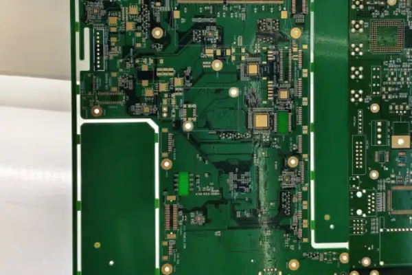
Recently, while discussing AI server PCBs with some hardware friends, I noticed an interesting phenomenon: many people focus on layer count and order. However, what truly tests a manufacturer is their ability to handle the unseen details.
I’ve seen some products with impressive design parameters that performed poorly in actual applications. Sometimes, problems arise in the most basic lamination process. The difference in the coefficients of thermal expansion between different materials is more subtle than imagined. During a factory visit, I once saw technicians repeatedly testing lamination parameters more than ten times before finalizing the solution.
When choosing a PCB supplier, I prioritize the rigor of their quality control processes. I once worked with a small factory whose prices were very competitive, but the delivered products always had minor deformation issues. Later, we discovered that their aging test process was inadequate.
Many manufacturers now advertise their ability to produce high-end HDI boards, but few can actually consistently control the precision of multiple lamination processes. One client, attracted by a lower price, chose a new factory, only to find during mass production that misalignment of the inner layers rendered the entire batch of boards unusable, resulting in higher costs.
Material stability is the key factor determining the upper limit. Adjusting the formulation of high-end resin materials often requires accumulating a large amount of experimental data, which cannot be solved by simple imitation.
Truly excellent PCB manufacturers establish their own failure analysis databases, turning each case into an opportunity to optimize the process. This ability for continuous improvement is more important than simply pursuing technical parameters; after all, reliability is the lifeline of industrial products.
I think many people’s understanding of AI servers is still superficial. When people talk about high-performance computing, they only focus on the GPU chip itself, ignoring the crucial factors that truly determine whether computing power can be fully realized—the circuit boards and interconnect layers that support the chip.
I’ve seen too many top-tier servers perform poorly in real-world operation, and the problem often lies in the signal transmission process (link/stage). Even the most powerful GPU, if it encounters a poorly designed circuit board, is like a sports car driving on a bumpy road—it simply can’t accelerate. This is especially true when handling massively parallel computing, where thousands of computing units work simultaneously, placing extremely stringent requirements on power stability and signal synchronization.
Last year, I debugged a cluster where the same A100 chip performed with up to 30% different performance on servers from different manufacturers. Disassembly revealed that the difference mainly stemmed from the circuit design of the GPU accelerator cards. Some manufacturers, in an effort to save costs, are still using the motherboard design approach of ordinary servers for AI servers, which is completely unacceptable. When eight GPUs are running at full speed simultaneously, the current fluctuations are comparable to the instantaneous startup of a small factory; ordinary power supply designs simply cannot withstand such an impact.
The truly professional approach is to design the entire system as an organism. Starting with the bottom-level packaging substrate, thermal expansion coefficient matching must be considered; otherwise, solder joints may crack when the chip operates at 70-80 degrees Celsius. The middle-layer PCB requires impedance control like designing precision instruments; even a difference of a few ohms can cause signal distortion. The most extreme case I’ve seen was a clock signal missynchronization that doubled the inference task’s time.
Some teams are now investing more of their budget in infrastructure optimization. This includes using thicker copper foil to reduce impedance, shielding and isolating critical signal lines, and even designing independent power supply modules for different computing units. These improvements may seem insignificant individually, but combined, they can improve system stability by an order of magnitude.
Ultimately, the competition in AI servers has shifted from front-end computing power to back-end engineering implementation. Like assembling a high-performance race car, a powerful engine alone isn’t enough; a matching transmission system and chassis tuning are also necessary. The idea that simply stacking the most powerful chips will win the race is increasingly unworkable in practice.
Every time I see those complex server configuration diagrams, I wonder if people are complicating a simple problem. Last week, while helping a friend’s company debug their AI server, I discovered that their expensively purchased equipment was being slowed down by a single, ordinary motherboard.
The core of an AI server is to facilitate smoother data flow, not to pile on the most expensive components. Those CPUs and GPUs touted as high-end, if not properly coordinated through motherboard design, are like building an eight-lane highway but leaving only a single lane at the entrance. I’ve seen too many companies blindly pursue top-of-the-line GPUs while neglecting the quality of the PCBs connecting these chips, resulting in idle computing resources.
The real performance bottlenecks are these seemingly insignificant connecting components. For example, if the switching chip, which coordinates multiple GPU modules, has substandard surrounding circuit board materials, high-speed signal transmission will be like a traffic jam, constantly retransmitting data. In this situation, even the best processor won’t perform as expected.
Interestingly, many manufacturers only emphasize processor performance in their marketing, rarely mentioning the underlying architecture supporting these chips. This is like boasting about the power of a sports car engine without mentioning whether the gearbox is compatible. Especially now, with AI computing demanding increasingly higher data transmission speeds, ordinary circuit boards simply cannot withstand continuous high-load operation.
I remember once during debugging, I discovered frequent system errors, and the problem turned out to be a seemingly ordinary power management board. Because it had to power multiple GPU modules simultaneously, the board’s thermal design was inadequate, leading to unstable voltage. Replacing it with a board with better thermal conductivity solved the problem.
Ultimately, the reliability of an AI server depends on its weakest link. Instead of obsessing over the parameters of a single chip, focus on the overall system’s synergy. After all, even the most powerful CPU needs a suitable motherboard to work with, and even the most advanced GPU relies on a high-quality PCB for connection. Next time you choose equipment, asking about the details of these connecting components might be more valuable than simply looking at the processor model.
I’ve been closely following the changes in the AI server field lately. Many people might think AI is all about software—algorithms and models are the key. But if you think about it carefully, you’ll find that hardware is just as important as software.
Take the PCB, for example. Traditionally, it’s just a board connecting electronic components, but now it has become one of the key factors affecting the performance of the entire system.
Especially as AI models grow larger and require increasingly more computing power, the demands on servers rise accordingly.
I remember chatting with a hardware friend once, and he mentioned that the biggest headache when designing AI servers is handling high-speed signal transmission. The sheer volume of data means even minor interference can degrade performance.
This makes PCB quality extremely important—not just material selection, but also wiring precision and even heat dissipation design.
Furthermore, the trend is towards more companies customizing their own AI chips, such as Google’s TPU or Amazon’s Inferentia. These chips have different hardware requirements, further driving innovation in PCB technology.
I think this reflects a deeper shift: in the past, hardware development often followed general needs, but now, with the emergence of specific applications like AI, hardware design is becoming more personalized and scenario-based.
For example, if you look at high-end AI servers, you’ll find their PCB designs are vastly different from ordinary servers—more layers, denser wiring, and more sophisticated materials.
The underlying reason is that AI tasks have extremely high latency and bandwidth requirements, which ordinary designs simply cannot meet.
So you see, while everyone talks about how powerful AI algorithms are, actually running these algorithms relies on the underlying hardware.
And the PCB, as the bridge connecting various chips, is playing an increasingly crucial role.
Sometimes I think this is a characteristic of technological development—the more fundamental something is, the more easily it is redefined during changes.
Previously, no one would have imagined that a circuit board could have so many variations, but now it has become one of the key factors determining the upper limit of computing power.
Of course, this also brings new challenges to hardware companies, because customer demands are becoming increasingly diverse, requiring sufficiently flexible design capabilities to keep up.
However, from another perspective, this change is quite interesting; it has revitalized the previously traditional hardware industry.
Anyway, I think the competition in AI servers will definitely become increasingly fierce in the next few years, and the innovation speed of PCBs, as a crucial component, will likely accelerate.
After all, the demand for computing power is there; if the hardware can’t keep up, even the most powerful software is useless.
Every time I see discussions about the internal structure of AI servers, I think about how many people overlook the most fundamental element: the platform that supports these complex calculations, especially the seemingly insignificant yet crucial GPU module board. This component is like the skeleton of the entire system; if it’s not robust enough, even the most powerful chip won’t perform to its full potential.
I’ve seen many projects focus too much on the GPU’s computing power during initial planning, neglecting the importance of the PCB as the supporting platform. As a result, various stability issues arise during actual deployment. Sometimes, a seemingly simple signal interference problem might require a complete redesign of the circuit layout. This made me realize that every aspect of AI hardware needs equal attention.
Speaking of the specific manufacturing process, the core circuit boards that connect to the GPU do require special treatment, especially when handling high-speed signals. Ordinary materials are often insufficient. I remember a project I participated in where improper material selection caused signal attenuation to exceed expectations. The problem was only solved by switching to a substrate specifically designed for high-speed applications. These details often determine the success or failure of the entire system.
More The design of the PCB layer is also a very interesting topic. Modern AI accelerator cards often integrate multiple GPUs, which places higher demands on the number of layers and the PCB structure. I appreciate the use of a stepped design approach, optimizing signal paths through interconnects at different levels. Although this increases manufacturing complexity, the investment is worthwhile in terms of long-term operational stability.
Another often overlooked point is the coordination between thermal design and circuit layout. In high-power computing environments, focusing only on chip heat dissipation while neglecting the PCB’s own thermal management can easily lead to localized overheating. I recommend considering the overall heat flow path during the design phase, ensuring the thermal solution and circuit layout form an organic whole.
In my experience, the best design often doesn’t pursue the ultimate in a single metric, but rather finds a balance between performance stability and cost. Sometimes, a seemingly ordinary design can bring more reliable performance—this is probably the most interesting aspect of engineering practice.
Every time I see articles discussing AI server PCB materials and getting bogged down in Df/Dk values, I want to laugh. Do you really think reducing dielectric loss by a fraction of a second can solve signal integrity issues? After working on over a dozen AI server projects, I’ve realized that copper foil selection is the truly underestimated key factor. Last year, while debugging a training cluster, I encountered a strange problem—with the same design, some nodes could reach 400Gbps, while others frequently experienced packet loss. After two weeks of troubleshooting, I discovered the issue stemmed from different batches of copper foil. To control costs, the supplier had secretly mixed in ordinary copper foil, causing some boards to exceed the surface roughness standard by 3 micrometers. This imperceptible difference resulted in a 15% attenuation of high-frequency signals. Replacing the entire line with the specified low-roughness copper foil immediately resolved the problem. The microstructure of the copper foil directly affects conductivity under the skin effect, especially in PAM4 signal systems above 112Gbps. Excessive roughness exacerbates signal edge jitter. This is like a sudden layer of fine sand on a highway; although it appears smooth, the tire grip has subtly decreased.
Currently, there’s a misconception in the industry that glass cloth is always considered a secondary component. However, when the number of PCB layers exceeds 30, the coefficient of thermal expansion of the glass cloth directly determines whether the board can withstand long-term high-load operation. I’ve seen too many cases of microcracks in the inner layers caused by CTE mismatch, ultimately forcing the scrapping of entire batches of boards worth millions. For example, in heat dissipation cycles with temperature differences exceeding 80°C, if the difference in the coefficient of thermal expansion between the glass cloth and the copper foil exceeds 2 ppm/°C, stress cracks will form at the blind vias after 3,000 thermal cycles. This damage spreads in a spiderweb pattern during X-ray inspection and is initially undetectable by conventional electrical tests.
Speaking of ultra-thin materials, everyone is currently chasing Japanese manufacturers’ copper foil, but have you tried domestic alternatives? Last month, we tested an 8μm copper foil from a local manufacturer on a 108-layer board, and it actually performed more stably than imported products—because their roughening process better matches the flow characteristics of the modified epoxy resin. Of course, this customized solution requires repeated adjustments to the lamination parameters with the factory; it’s not something you can just buy a standard product for. During actual lamination, the temperature rise curve must be controlled within the range of 2-3°C per minute to allow the resin to fully fill the microcavities formed by the uneven surface of the copper foil. We used scanning electron microscopy to compare and found that the nodular crystal distribution of domestically produced copper foil was more uniform, which allowed us to control the dielectric layer thickness fluctuation within ±1.5μm.
The real test of design skill lies in balancing material performance and processing difficulty. For example, using T-glass can indeed improve performance, but the yield rate may drop below 60%. In this case, we need to judge whether it is worth sacrificing production capacity for those slight parameters. Once, to meet a project deadline, we deliberately chose the more mature E-glass and delivered samples three weeks ahead of schedule by optimizing the wiring rules. Specifically, we avoided the stress concentration zone of 15mm on the board edge for critical signal lines and used a 45° oblique wire arrangement to offset the difference in strength between the warp and weft directions. This empirical adjustment allowed us to achieve more stable impedance control on ordinary materials than on high-end materials.
I think the biggest problem in the industry right now is that there is too much reliance on parameter specifications. I’ve seen too many teams take the impressive data provided by material suppliers and start working directly, only to fail during actual assembly due to compatibility issues. I recently helped a friend troubleshoot a case. They were using Low-DK PCBs with impressive specifications, but the issue stemmed from electromagnetic interference (EMI) generated when the PCB resonated with other components inside the server chassis. This kind of dynamic problem is rarely mentioned in the specifications. For example, when a cooling fan’s specific speed coincides with the PCB’s natural frequency, it can induce millimeter-level mechanical vibrations. These micro-vibrations can cause periodic fluctuations in transmission line capacitance.
Ultimately, AI server PCB design is more of an empirical science. Instead of blindly pursuing the latest materials, it’s better to first thoroughly understand the limitations of existing processes.
Sometimes, fully exploring the potential of ordinary materials is more reliable than risking using immature new technologies. Just like an experienced chef can create a delicious dish from ordinary ingredients, the key lies in controlling the heat, not blindly pursuing rare ingredients. Our team is currently building a materials failure case library, recording the performance of each material under extreme conditions as a “failure map.”
I always laugh when I see articles discussing AI server hardware emphasizing how powerful the technical parameters are. Anyone who has actually deployed such systems knows that even the most powerful hardware is only part of the basic configuration.
I’ve seen too many teams pour their budgets into purchasing top-of-the-line GPUs, only to see overall efficiency decline.
I remember last year helping a company optimize its architecture. They were using flagship-level accelerator cards, but data processing speeds just wouldn’t improve. Later, we discovered the problem lay in the carrier board’s signal transmission design. Those modules supposedly supporting high-speed communication were experiencing a surge in packet retransmission rates due to impedance mismatch issues. On the surface, each GPU seemed to be running at full capacity, but in reality, a third of the time was spent processing error correction.
Many manufacturers like to boast about the number of high-end materials used in their AI server PCBs. However, I believe that more layers actually increase the likelihood of problems. I once tested a 26-layer accelerator card, and after 72 hours of continuous operation, uneven heat dissipation caused micro-deformation, leading to poor contact between the GPU and memory. This kind of problem is impossible to detect in a laboratory environment.
Truly stable systems often need to find a balance between performance and reliability. For example, some mid-range carrier boards, although theoretically having 15% less bandwidth than top-tier models, excel in signal integrity control, resulting in more stable actual throughput.
Some customers are obsessed with the computing power figures of individual GPUs, neglecting the efficiency of cluster collaboration. During the debugging of an eight-card system, I found that although each accelerator card scored impressively individually, due to a design flaw in the switching module, the latency fluctuations during data synchronization between GPUs were unbearable.
Ultimately, hardware is just a tool; the key is the overall architecture’s compatibility. Like building blocks, simply stacking the most expensive parts doesn’t create a skyscraper. Sometimes, a simplified design can bring more predictable performance, which is what truly deserves attention in engineering practice.
That day, while debugging a newly designed board in the lab, I suddenly realized an interesting phenomenon—engineers designing AI server PCBs seem to be caught in a vicious cycle. Everyone is frantically pursuing higher-layer HDI designs and impressive numbers on material specifications for lower losses, neglecting the most fundamental aspects. I’ve seen too many teams pour their budgets into high-end materials, only to have the entire batch of boards experience inexplicable signal interference due to improper grounding.
A project I participated in last year left a particularly deep impression on me. The client insisted on using a major manufacturer’s latest ultra-low-loss substrate, but during the first batch of sample testing, the power supply noise was actually 30% higher than with ordinary materials. Later, we discovered the problem lay in a very small detail—in pursuit of higher wiring density, they placed several critical decoupling capacitors directly below the heatsink holes. This seemingly insignificant layout error directly compromised power integrity, yet no one noticed this detail during initial simulations.
In fact, the most dangerous thing in AI hardware development is this kind of putting the cart before the horse. Now, the industry is full of talk about 16-layer and 24-layer boards, but few are willing to spend time studying basic topologies. I’ve handled many rework cases where the problem stemmed from the simplest impedance matching. A client once brought me two PCBs from different manufacturers, asking why the one with worse specifications actually had better transmission stability. Upon closer inspection, I discovered the secret to the winning board lay in its more efficient use of equal-length traces—although the material was ordinary, the length error of each differential pair was controlled within 5 mils.
Recently, while evaluating suppliers for a friend’s company, I encountered a similar issue. Both companies could provide so-called high-end AI server PCBs, but one overemphasized material specifications, while the other showcased their special optimization solutions for heat dissipation. We ultimately chose the latter because they could clearly explain the actual impact of each via location on thermal management, rather than just discussing theoretical values. This reminded me of my early experience designing communication base stations—sometimes solving signal integrity problems doesn’t require cutting-edge technology, but simply a thorough understanding of existing stack-up solutions.
The true test of an engineer’s skill often lies not in using the most expensive materials, but in creating the most stable design within a limited budget. Just last week, I saw an interesting design where they improved high-frequency performance by 15% on ordinary FR4 material by optimizing copper foil roughness. This pragmatic approach demonstrates technical strength more effectively than blindly chasing new technologies, since the reliability of AI servers ultimately depends on actual operational performance, not on fancy data sheets provided by material suppliers. I always laugh when I see promotional videos for AI servers that claim to deliver astronomical computing power. They love to show off the flashing lights in the racks but rarely mention the thing behind the scenes that truly determines success or failure—the PCB board that houses all the computing cores. Do you know what’s most ironic? Those trillions of calculations per second are actually built on the most basic laws of physics, and the power supply is the most vulnerable link.
I’ve seen too many teams spend all their energy on algorithm optimization, only to stumble on the simplest power supply problem. One image recognition project’s AI server frequently made misjudgments during testing; it was later discovered that a faulty capacitor selection caused the processor’s response speed to lag when voltage fluctuated.
The power consumption fluctuations of AI chips now are like a rollercoaster—one second they might be in standby mode, and the next they’re running at full load. This instantaneous surge of current is like a mini-hurricane for the power system. No matter how perfect the power layer design is, if the decoupling capacitors aren’t keeping up, the entire system will suffer.
The real test of an engineer’s skill is how to make those seemingly ordinary capacitors function at critical moments. Many people believe that simply piling on components solves the problem, but layout is more important than quantity. Placing a high-frequency capacitor three centimeters away from the chip might not be as effective as placing a regular capacitor right next to the pins. Current doesn’t wait for you; it needs the shortest path.
I remember once disassembling an AI server from a major international manufacturer; their PCB layout was like a work of art. The copper foil on the power path was noticeably thicker, and the capacitors at critical nodes were arranged as neatly as piano keys. This reflects a deep understanding of current characteristics—the voltage drop generated when a large current flows through a conductor can significantly reduce chip performance.
Thermal design is another crucial aspect. The heat generated by these high-power chips must ultimately be conducted away through the PCB. I’ve seen designs that, in pursuit of layer compression, completely block out heat dissipation channels, resulting in machines throttling after less than ten minutes of operation.
Ultimately, designing an AI server PCB is like building a track for a group of sprinters. You need to ensure their explosive power at the start while considering stability during continuous running; any flawed detail will prevent even the most powerful computing capabilities from being realized.
Sometimes I feel that this industry is too focused on cutting-edge technology and has forgotten to look back at these fundamental aspects. True performance breakthroughs often lie hidden in seemingly ordinary power supply designs and heat dissipation solutions. Teams that master capacitor placement are the ultimate winners.
What do you think? Have you encountered similar situations?
I think many people’s understanding of AI servers is somewhat skewed. They focus on fancy algorithms and software architectures, neglecting the most fundamental element—the PCB. You might think a circuit board can’t be that technically complex, but anyone who has actually worked with hardware knows it’s the key to system stability. I’ve seen many projects suffer from frequent system failures due to poor PCB design.
Take impedance control, for example. It’s not as simple as just drawing a few lines. High-frequency signals are particularly sensitive during transmission; a difference of a fraction of a millimeter in line width can cause signal reflection problems. Once, our team was debugging an AI server project. Even though all the chip parameters were correct, data transmission was unstable. We later discovered that the impedance near a via on the PCB wasn’t properly matched.
Signal integrity is even more of a headache. Modern AI servers handle data streams of tens of Gbps. At this speed, any interference on the PCB can cause data packets to malfunction. Some engineers like to cram high-speed lines too close together, resulting in severe crosstalk and a chaotic, noisy environment.
In fact, good PCB design is like building a highway for data; it requires both a smooth surface and adequate safety barriers. Manufacturers who boast about using top-tier chips but are unwilling to invest in PCB design often perform only moderately in real-world applications.
I increasingly feel that AI hardware development shouldn’t be judged solely by surface-level specifications. Sometimes, the most basic material choices and wiring techniques reveal a team’s true capabilities. After all, even the most sophisticated AI algorithms need a reliable circuit board to support their computational power.
Recently, I chatted with some hardware friends about the current AI boom and noticed an interesting phenomenon: everyone is discussing the power of GPUs and the size of model parameters, but few pay attention to the foundation supporting these behemoths—the PCBs lying in the chassis. If you think about it carefully, with each iteration and upgrade of an AI server, it’s actually these seemingly insignificant circuit boards that bear the brunt of the stress.
I remember last year when I was helping a data center with an upgrade, their existing ordinary servers frequently experienced signal attenuation when handling AI loads. Later, we switched to a server model specifically optimized for AI. The most obvious improvement was the redesign of the PCB layers and materials. This made me realize that when data needs to travel between GPUs at speeds of hundreds of gigabytes per second, traditional circuit board designs can no longer keep up with the demands.
A friend who works in R&D shared their experimental data with me: when training large language models, the need to frequently synchronize parameters between multiple GPUs places extremely high demands on interconnect bandwidth. If the PCB impedance control is not done well, or if the heat dissipation design is flawed, the efficiency of the entire system will be significantly reduced. They had tested AI servers from different manufacturers and found that performance differences largely stemmed from the design details of the circuit boards.
Many manufacturers are now promoting so-called “wireless” architectures, which is indeed a direction. But I think what’s more important is how to make the PCB itself the main channel for data transmission. Like urban traffic, instead of constantly building overpasses (cables), it’s better to design the main roads (PCBs) to be wider and smarter. After all, in AI computing scenarios, data flow is no longer a simple point-to-point transmission, but a complex network of interactions. For example, in the latest AI servers, the PCB needs to integrate thousands of high-speed differential pairs, and the loss of each channel must be controlled within 0.5dB/inch. This places unprecedented precision requirements on wiring and lamination processes.
I’ve noticed some startups starting to focus on the substrate of the PCB, such as trying new resin materials to improve high-frequency performance. This approach is clever because instead of patching things up within the existing framework, it’s better to fundamentally rethink material selection. This reminds me of the transition from LCD to OLED screens when smartphones first became widespread—sometimes breakthroughs are hidden at the most basic level. Specifically, they are testing composite materials with low dielectric constant (Dk) and low loss factor (Df), which can maintain stable performance above 40GHz, laying the foundation for future terabit-level interconnects.
Of course, the challenges are significant. As the number of layers increases, heat dissipation and mechanical strength must be reconsidered. Once, I visited a supplier’s factory and saw them testing high-multilayer boards: not only must signal integrity be guaranteed, but they must also withstand long-term high-load operation. This is like building a sports car—it needs to be both fast and durable. Their thermal management solution includes embedded copper pillars and microchannel liquid cooling technology, ensuring an operating temperature below 85°C even with a heat density of 500W/cm².
Looking to the future, I believe the evolution of AI servers will increasingly rely on breakthroughs in PCB technology. As computing power density continues to increase, how to arrange more computing units within a limited space while ensuring their efficient collaboration is essentially an art of hardware layout. Perhaps in a few years, we will see server architectures completely different from today’s—PCBs may no longer be simple connection carriers, but will become true “neural network skeletons.” For example, through 3D stacking technology and through-silicon vias (TSVs), a single substrate can support the optoelectronic hybrid interconnection of heterogeneous computing units, achieving integrated memory and computing.
The other day, while looking through old photos, I suddenly realized an interesting phenomenon—ten years ago, we were still discussing whether mobile phones could replace computers for office work! Now even roadside stalls use QR codes for payment. This speed of technological penetration has given me a new perspective on the currently hotly debated topic of AI. Many people imagine AI as a magic wand floating in the clouds, but it’s more like the blood flowing through countless physical devices, and the vascular system carrying this blood is those seemingly ordinary circuit boards.
I remember visiting a data center last year, and an engineer pointed to the blue-glowing devices in the racks, saying that one row was dedicated to medical image analysis, and another row was responsible for training autonomous driving models. Looking closer, I realized that the internal structure of each server was far more complex than I had imagined, especially those boards covered with intricate circuitry that had to simultaneously handle high-frequency signal transmission and heat dissipation challenges. This reminded me of when I was a child assembling a radio; breaking a single wire would ruin the whole thing. Now, these circuits handling massive amounts of computation have almost zero fault tolerance.
A friend who works in hardware complained to me that when they were testing a new model, they found that conventional cooling solutions couldn’t handle the heat generated by high-intensity computation. They had to adjust the layout of the components on the board to solve the problem. These details may seem insignificant to outsiders, but they directly affect the stability of the entire system. It’s like building a house; if the foundation is crooked, no matter how beautiful the decorations are, it’s all for nothing.
I’ve observed a phenomenon: many discussions focus on algorithm optimization, but when it comes to actual implementation, hardware bottlenecks often become an invisible ceiling. For example, some AI applications require real-time processing of massive amounts of data. If the signal transmission speed inside the server can’t keep up, even the smartest algorithm will be stuck waiting. It’s like putting a bicycle chain on a sports car—it looks cool, but it’s frustrating to run.
Recently, I’ve noticed some manufacturers starting to experiment with new materials for circuit boards, which is an interesting direction. Traditional materials are prone to deformation under high loads, like a chocolate cake under high heat, but the application of innovative materials could potentially increase the durability of the entire system by an order of magnitude. However, such attempts need to balance cost and performance; after all, businesses won’t just pay for concepts.
Ultimately, technological development is always a spiral process. Before the widespread adoption of personal computers, some people doubted whether ordinary households needed computers. Looking back now, that doubt seems so short-sighted. For the rapidly evolving AI infrastructure, perhaps we should take a longer-term view; every improvement today paves the way for future possibilities.
Every time I see teardown diagrams of high-end AI servers, I always think about one question: why are some manufacturers willing to spend three times the cost to customize special PCBs? There’s actually an easily overlooked logic behind this—when computing power density exceeds a certain critical point, conventional designs become ineffective.
The most extreme example I’ve seen is a single, palm-sized board integrating four H100 chips. Engineers had to design each chip individually. The power supply module is like providing four high-powered engines with their own dedicated fuel systems. This design is completely invisible in ordinary servers because the power consumption curve of a typical CPU is relatively flat, while an AI chip can experience instantaneous load changes, such as jumping from 200 watts to 700 watts within milliseconds. This kind of instantaneous load change causes the copper layers of a traditional PCB to deform slightly, like a heated wire.
Speaking of material selection, there’s an interesting phenomenon in the industry: Even though it’s known that M9 grade boards are ten times more expensive than ordinary FR4, leading manufacturers are still vying to use them. At a technology exhibition last year, a senior engineer gave an analogy—it’s like driving on a highway. Ordinary materials are like a gravel road; at 150 km/h, the car will become unstable, while ultra-low loss materials are like an asphalt racetrack, allowing signals to travel at 0.9 times the speed of light without distortion. Especially for clock signals that require long-distance transmission, a difference of milliseconds can lead to vastly different results.
Electromagnetic compatibility (EMC) issues are actually more challenging than imagined. Once, during testing of a server, we discovered that the GPU’s bit error rate spiked whenever the server room air conditioning was activated. We later found a flaw in the power supply filter module’s grounding design; the return current path was detoured, like a river suddenly changing course, easily causing flooding. The final solution was to add a copper foil mesh to the back of the PCB, providing a shortcut for interference currents. This detail, invisible on the schematics, directly determines system stability.
Innovations in heat dissipation design are also interesting. The most cutting-edge approach now is to embed microchannels inside the PCB, like capillaries running through the entire board. During a lab visit, I saw them demonstrate using a semi-transparent composite material. When hot water flowed through, it was clear how heat was instantly carried away from under the chip. The temperature difference between the inlet and outlet was less than 3 degrees Celsius. While this design is difficult to manufacture, it’s far more fundamentally effective than external heat sinks for AI training clusters operating at full load for extended periods.
Ultimately, AI server PCBs are no longer simply connection carriers; they’re more like the nervous system of a precision instrument, needing to conduct signals, resist interference, and manage energy flow. Behind those seemingly over-designed choices lies hard-won experience gained through painful lessons.
Circuit boards are more than just that green board in a phone
From disassembling old routers to visiting electronics manufacturing plants, I gradually realized
As an electronics enthusiast, I’ve come to understand firsthand the impact of
- 중소규모 배치 생산 전문가
- 고정밀 PCB 제작 및 자동화된 조립
- OEM/ODM 전자 프로젝트를 위한 신뢰할 수 있는 파트너
영업 시간: (월~토) 9:00~18:30