

What Documents Are Required for PCB Production: A Field Guide From Real Industrial Weighing Controller PCB Projects
Many engineers focus too much on technical parameters early on and overlook
I recently dug out an old project board I did a few years ago, and looking at the densely packed circuits on it suddenly brought back some memories. I remember when I first started learning electronic design, I always felt that turning circuit diagrams into physical objects was a particularly magical thing, especially for those boards that required multilayer structures.
Once, to rush a prototype, I spent an afternoon chatting with the masters at a local PCB factory. In that workshop filled with the smell of chemicals, the veteran craftsman pointed to the boards being laminated and said, “Don’t be fooled by how thin this thing is; it’s just a card in the end. There are over a dozen layers of intricate details hidden inside and out.” This reminded me of my later experience working on four-layer PCBs—just getting the inner layers aligned took three reworks. Every time I saw a board with misalignment after etching, I wanted to smash my microscope.
Many people’s impression of multilayer PCBs is still stuck on the idea that “the more layers, the more advanced.” But what truly determines performance are often those unseen details: for example, poor control of the prepreg’s flowability can lead to uneven interlayer thickness, and incorrect drilling parameters can damage the copper foil. These intricacies hidden in the manufacturing process are far more crucial than simply stacking layers.
I experienced this deeply last year when helping a friend modify a drone flight control board. The original design used a six-layer board, but it was later discovered that by adjusting the copper plating of the power layers, a four-layer structure could achieve the same anti-interference effect. This made me realize that sometimes blindly pursuing a higher layer count can mask the real problem—like focusing on painting the walls during home renovations while forgetting to check the structural integrity of the load-bearing walls.
Now, I can’t help but laugh when I see advertisements using “20-layer PCB” as a selling point. The number of layers is never the goal; the key is whether each layer can work together seamlessly. Just like a good team doesn’t need a large number of members, the important thing is whether the members can form effective connections. Next time you design a circuit, ask yourself: is this extra layer to solve a problem, or just to satisfy vanity?
I’ve always felt that many people overcomplicate multilayer board manufacturing. In fact, the fate of the entire board is determined from the very first core. I remember once visiting a factory and seeing workers moving those copper-clad laminates, and I suddenly realized that these seemingly ordinary materials are the starting point of the whole story.
You might wonder why the core needs to be pre-cured. This is like building a house—you need to lay a solid foundation first. If the foundation layer is unstable, all sorts of problems will arise during the lamination process. I’ve seen novice engineers choose inferior cores to save costs, resulting in delamination and scrapping of the board after lamination.
When it comes to copper foil selection, many people only focus on thickness while ignoring surface treatment. Once, we tested copper foil from different manufacturers and found that even with the same thickness, differences in roughness could lead to drastically different signal integrity. These details are often invisible on schematics.
The most fascinating part of the lamination process is the slow melting of the translucent adhesive sheet at high temperatures. It acts like glue, bonding the core layers together, but even slight deviations in temperature control can cause uneven resin flow. I’ve personally witnessed cases where inner layer circuitry was deformed due to excessively rapid heating—it was truly heartbreaking.
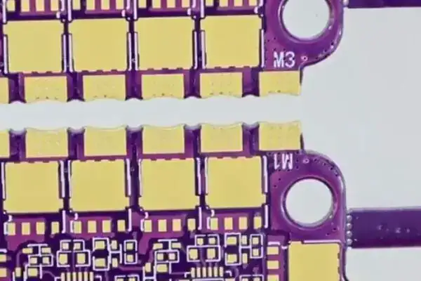
Actually, the best way to understand multilayer PCB manufacturing processes isn’t by looking at flowcharts, but by touching the difference between the board before and after lamination. When you feel how the smooth copper foil and solid cores solidify into a unified whole, you truly understand what “layers interlocking” means. This tactile experience is far more intuitive than any textbook diagram.
Sometimes I feel that board manufacturing is quite similar to cooking; a slight difference in heat can completely change the flavor. The only difference is that we’re using temperature profiles and pressure parameters, not seasonings.
I’ve seen many engineers neglect manufacturing processes during the design phase. Once, our team took on a project where the client insisted on using exceptionally thick copper foil for the power layer. The resulting sample showed severely wrinkled copper foil, resembling crumpled paper. This problem often stems from not considering the differences in thermal expansion coefficients during lamination. In fact, manufacturing multilayer boards is like assembling building blocks, requiring precise alignment.
Many people think that once they’ve drawn the circuitry and handed it over to the factory, everything is fine. But after working on several projects, you’ll find that the same design can produce vastly different results in different factories. I remember once designing a board that required an extremely thin dielectric layer to meet impedance requirements. During testing, we discovered signal integrity issues, later finding that uneven pressure during lamination caused variations in dielectric layer thickness.
My current habit is to hold a brief conference call with the manufacturing plant’s technical staff early in the design process. We go over key parameters such as linewidth, spacing, and dielectric thickness, and listen to their actual production experience. Once, when we wanted to use a new type of prepreg material, the factory’s process engineer directly reminded us that this material had strong fluidity during high-temperature pressing, requiring design adjustments to compensate for this. This avoided potential quality problems.
In fact, understanding manufacturing processes isn’t about becoming a production expert, but about making designs more practical. For example, when choosing via types, knowing the cost difference between mechanical drilling and laser drilling allows for optimized design solutions while ensuring performance. Sometimes, slightly adjusting the wiring can save a lot of trouble later, which is much more cost-effective than reworking after problems arise.
I think the thing designers should avoid most is working in isolation. With new materials and processes constantly emerging, maintaining a learning attitude is important, but even more important is applying theoretical knowledge to specific designs. After all, even the best ideas need manufacturing processes to become usable products.
I’ve seen many people who are particularly curious about the circuit board manufacturing process. Actually, the production process of multilayer PCBs is quite interesting. It’s not like stacking layers like making a cake; it’s more like playing a jigsaw puzzle. Every time I see those complex circuit patterns, I think engineers have perfectly combined art and technology.
I remember once visiting a factory and seeing workers processing a board that was about to be completed. The dense network of lines reminded me of a city’s transportation network, except here the “roads” are paved with copper foil. One of the most critical steps in the manufacturing process is ensuring the alignment precision between each layer; even a millimeter’s difference can ruin the entire board.
Speaking of multilayer PCB manufacturing, what I find most fascinating is its “inside-out” construction method. It starts with the core layer in the center and expands outwards like building blocks. This process requires extremely precise temperature control and pressure adjustment; otherwise, air bubbles or poor adhesion between layers can easily occur.
I once encountered a particularly interesting example. A friend designed an audio processing board, but the first batch always had noise. It was later discovered that the signal and power lines on one layer were too close together, causing interference. After readjusting the wiring spacing, the problem was solved. This illustrates that even seemingly simple layout details can have a significant impact on actual production.
Now, many electronic products are pursuing thinner and lighter designs, which places higher demands on multilayer board manufacturing. I’ve noticed that some manufacturers are starting to use more precise laser drilling technology to handle those micro-holes that are almost invisible to the naked eye. This technological advancement allows designers to achieve more complex circuit layouts.
In fact, observing a finished circuit board reveals many details about the manufacturing process. For example, the smoothness of the edges and the flatness of the hole walls reflect the factory’s craftsmanship. Sometimes, you can even determine the surface treatment process from the color of the solder pads.
I think understanding these manufacturing details is particularly helpful for designers. When you understand the process limitations of each step, drawing schematics becomes much more targeted. After all, even the best design needs to be feasible.
Recently, I’ve seen some emerging flexible circuit board technologies, and I feel this will be the next direction of development. Traditional rigid circuit boards do have limitations in certain special scenarios, while flexible substrates may open up new application areas. However, these new materials present entirely new challenges to the manufacturing process, requiring the entire industry to explore solutions.
Every time I encounter a new circuit board design, I pay special attention to its interlayer structure. Some designs seem simple but actually contain hidden intricacies, such as those cleverly utilizing intermediate layers for heat dissipation or shielding. These details often determine the final performance of the product.
Speaking of quality control, I think the most easily overlooked aspect is material consistency. Different batches of substrates may have slight differences, and these differences are amplified when multilayer boards are stacked. Good manufacturers have strict incoming material inspection processes to ensure that each batch of materials meets standards.
I have always believed that circuit board manufacturing is an important bridge connecting creativity and reality. A good design needs to be transformed into a reliable product through excellent craftsmanship. This process requires close cooperation between designers and manufacturers. Both parties must understand each other’s working characteristics and limitations to create truly excellent products.
Watching a shiny substrate slowly transform into a fully functional circuit board is like watching a seed grow into a large tree. Every step is important and indispensable, and there is an interrelationship between the preceding and following processes. This is probably the charm of manufacturing.
When I first started learning circuit design, I always thought multilayer boards were something very mysterious. Back then, when I saw other people’s drawings of six-layer and eight-layer boards, I wondered—isn’t that just gluing several double-sided boards together? Later, after actually participating in a high-speed signal processing project, I realized how complex it was.
I remember being most impressed by the alignment process when I first saw the factory’s production workshop. Workers stacked dozens of paper-thin inner core boards together, then meticulously adjusted their positions using an optical positioning system. A difference of just a few micrometers could ruin the entire batch. This precision requirement reminded me of attaching airplane wings when building models, except here you can’t just use glue.
Many people think the difficulty of multilayer boards lies in the number of layers, but the real challenge is how to integrate these independent copper foil layers into a unified structure. I once witnessed the lamination process firsthand; the prepreg slowly melted and flowed under high temperature and pressure, filling the gaps between the circuits. The whole process was like making a mille-feuille cake, except that each layer had to be absolutely flat.
The material selection process is also quite interesting. Prepregs from different manufacturers vary greatly in fluidity; some are like honey, slowly seeping through, while others are like water, easily becoming uncontrollable. We once changed suppliers, causing the impedance values of an entire batch of boards to exceed the standard; we later discovered it was due to a subtle change in the dielectric thickness.
The drilling process requires more experience than you might imagine. Once, while monitoring production at a factory, I noticed a foreman adjusting the drill bit speed. Upon inquiry, I learned that different holes in different locations require different parameters—through holes near the board edge are prone to edge chipping, while blind holes in the middle are difficult to drill through. These details are completely absent from textbooks.
What surprised me most was the significant difference between impedance calculations in the design phase and actual production. Theoretically, the calculated striplines could deviate in production due to copper foil roughness, dielectric uniformity, and even the thickness of the green ink. Now, when communicating with engineers, I specifically emphasize impedance strip testing.
The most fascinating aspect of multilayer board manufacturing is that there’s never a perfect solution. Each project requires balancing specific signal requirements, cost budgets, and delivery dates. For example, sometimes, to control costs, we suggest clients change a ten-layer board to an eight-layer structure with two partially buried blind vias, which can actually save a considerable amount of money.
Looking back now, I realize how incredibly helpful understanding of manufacturing processes is for design. At least I no longer encounter situations where differential lines cross segmented areas and I blame the manufacturer for poor workmanship. After all, a good circuit board is the result of collaborative effort between design and manufacturing.
Every time I see those circuit boards covered in intricate circuitry, I wonder how they transform from a pile of raw materials into complex, multi-layered structures. Especially those seemingly simple through-holes, which actually bear the crucial responsibility of connecting different layers. I’ve seen workers in factories handling these details; they have to ensure every step is just right. For example, after drilling holes in insulating material, the hole walls must be treated extremely carefully to guarantee subsequent conductivity; otherwise, the entire board might be unusable.
I remember once visiting a workshop where a foreman pointed to a board that had just had holes drilled and said, “Look, these holes are still insulating. To make them conductive, they need special treatment first. A chemical solution is poured in, allowing copper to slowly deposit on the hole walls.” This process sounds simple, but in practice, temperature and time must be strictly controlled. Even a slight deviation can affect the reliability of the final product. That’s when I understood why some cheap circuit boards break down so quickly—it’s likely because they cut corners in this step.
Many people think that circuit formation is simply printed on by a machine, but it’s not that simple. First, photolithography is used to… The designed pattern is transferred to the board, and then the copper layer that needs to be retained is thickened through electroplating. The other areas are then etched away with chemical solutions. I’ve seen workers adjust the etching solution concentration; too high a concentration damages the lines that should be preserved, while too low a concentration leaves excess copper that can’t be cleaned. This balance requires experience and cannot be achieved solely through automated equipment.
Another small detail is the treatment of the solder mask layer. Don’t underestimate this seemingly simple application of green solder mask; it must be precisely applied over the lines while leaving space for solder joints. I’ve seen some shoddy factories cover the solder pads to save time, resulting in impossible soldering during assembly. These seemingly insignificant steps are actually the best indicator of a manufacturer’s professionalism.
Ultimately, manufacturing multilayer boards is like assembling building blocks; every step must be perfectly executed. From drilling to copper plating, from wiring to protection, nothing is dispensable. But what impresses me most is that many manufacturers, in order to meet deadlines, omit the repeated inspections that are essential in traditional processes, directly leading to a shortened product lifespan. Sometimes, going slower allows for greater longevity.
I’ve seen many people think of multilayer board manufacturing as incredibly mysterious and complex, but in reality, it boils down to just a few things. Take the inner layer fabrication as an example; the key is accurately transferring the pattern onto the copper surface.
I remember once visiting a factory to see them making circuit boards. Workers were applying photosensitive film to the substrate. The roll of pale yellow film unfurled evenly in the machine, like putting a protective suit on the circuit board. The flatness of the film application directly affects the subsequent image quality; this step, seemingly simple, requires a great deal of experience.
Imaging processes are becoming increasingly intelligent; LDI equipment can directly transfer patterns using laser scanning. However, traditional exposure machines also have their advantages, especially in terms of cost-effectiveness when producing large batches of standard boards. The choice between methods depends on specific needs; there’s no need to blindly pursue the latest technology.
The chemicals in the etching tank do have a strong smell, but watching the exposed copper foil precisely etch out the circuit outlines is always amazing; the precision brought about by the chemical reaction is astonishing. Once, I discovered burrs on the edges of a batch of boards, which turned out to be caused by fluctuations in the chemical concentration—so regularly checking solution parameters is crucial.
What impressed me most was the change after the browning treatment. The originally shiny copper surface turned a matte chocolate color, with a slightly frosted feel. This roughness is particularly critical for subsequent lamination, like adding an anti-slip mat between different floors. One customer once neglected this step, resulting in boards that delaminated during high-temperature testing.
In fact, the manufacturing process of multilayer boards is like building with blocks; each step lays the foundation for the final performance. Sometimes, the most inconspicuous details determine success or failure, such as the purity of the water in the cleaning process or the temperature and humidity control in the workshop. These seemingly trivial matters are precisely the key to ensuring yield.
A truly good board isn’t one that excels in any one aspect, but rather one where all processes perform consistently well. Just like a band performance, every musician needs to keep up with the rhythm.
I’ve always found the manufacturing process of multilayer boards particularly interesting. Many people might think it’s simply a matter of gluing several single-sided boards together, but it’s far more complex.
Take the drilling process, for example. Sometimes, seeing those densely packed tiny holes, you wonder how they precisely connect the circuitry of different layers. I’ve seen some factories pre-mark each layer with points, these points being as crucial as coordinates on a map. After all the layers are laminated together, technicians use X-ray equipment to locate these points, ensuring that the subsequent drilling positions are absolutely accurate.
Speaking of the lamination process for multilayer boards, I think the most technically demanding aspect is temperature control. Too high a temperature will cause material deformation, while too low a temperature will affect the adhesion. Once, I visited a factory and witnessed them adjusting the temperature profile of the laminating machine; the level of detail was like conducting a scientific experiment.
Regarding drilling technology, I’ve found that many people don’t understand the difference between mechanical drilling and laser drilling. Simply put, mechanical drilling is suitable for ordinary through holes, while laser drilling is better suited for handling tiny blind holes. I remember once receiving a sample board with laser-drilled holes finer than a human hair—it was truly astonishing how advanced the technology is now.
Before entering this industry, I never imagined cleanliness could be so important. I once saw workers undergoing several dust removal procedures before entering the workshop, even having to be careful about their breathing. Later, I understood that even a tiny speck of dust falling between the layers could ruin the entire board.
What I find most interesting is observing the changes in resin material at different temperatures. At room temperature, it’s solid; after heating, it becomes fluid, filling the gaps; and after cooling, it returns to a solid state, firmly bonding the layers together. This process is like witnessing the transformation of a material.
Speaking of the manufacturing process of multilayer boards, I particularly enjoy observing the workers’ handling of the boards. They treat each board like a work of art, proceeding with utmost care at every step. Sometimes I think it’s this attention to detail that ensures the reliability of the final product.
What I admire most about this industry is its spirit of continuous innovation. Every time I attend a trade show, I see new processes and equipment emerging, making the manufacturing of multilayer boards more precise and efficient. This makes me believe that future electronic products will become more powerful and reliable thanks to these technological advancements.
Many engineers focus too much on technical parameters early on and overlook
As someone who has worked in PCB outsourcing for years, I’ve found
Cramming a camera, amplifier, dual-mic array, and Wi-Fi radio into a palm-sized
- 중소규모 배치 생산 전문가
- 고정밀 PCB 제작 및 자동화된 조립
- OEM/ODM 전자 프로젝트를 위한 신뢰할 수 있는 파트너
영업 시간: (월~토) 9:00~18:30
Get quote, solution or any question, Andre always here to help