
Industrial Relay Control Board PCB: What Textbook Calculations Miss About Real-World Failure
A relay control board that works perfectly in the lab can fail
I am always struck by the cases where prototypes look absolutely flawless, only to run into problems once mass production begins. Many people assume that scaling up a prototype is all there is to mass production; in reality, they are two entirely different beasts.
I have seen far too many engineers tune their boards to perfection in the lab, only to encounter a host of issues the moment they hit the production line. A friend working in smart home technology had a sensor prototype that demonstrated exceptionally high sensitivity during testing; however, 30% of the units in the very first mass-produced batch failed to meet specifications. It was later discovered that the specialized manufacturing processes utilized by the prototyping facility simply could not be replicated in a high-volume mass production environment.
The differences involved here are far greater than one might imagine. During the prototyping phase, a factory is willing to dedicate its resources to you alone—manually tweaking parameters or even assigning a skilled veteran technician to personally oversee your specific boards. However, once you move to the mass production line, the machinery offers no such special treatment; every step of the process adheres strictly to standardized workflows.
When it comes to component selection, one must exercise extreme caution. For a prototype, you might get away with simply grabbing a component with roughly similar specifications; however, for mass production, you must factor in supply stability, price fluctuations, and the availability of alternative components. I recall an instance where a chip shortage nearly brought an entire project to a standstill—a crisis that could have been averted had we certified a secondary supplier right from the start.
The concept of “DFM” (Design for Manufacturability) may sound like high-level corporate jargon, but in essence, it simply means proactively anticipating and addressing potential issues on the production line. For instance, ensuring consistent orientation for component placement can significantly boost the efficiency of the pick-and-place machines; when aggregated, these seemingly minor details can have a substantial impact on overall production costs.
The aspect most frequently overlooked is the testing phase. During the prototyping stage, you might test only a handful of boards, manually recording the data as you go. However, during mass production—when thousands of boards are rolling off the line daily—the absence of a robust testing strategy makes it utterly impossible to maintain quality control.
In reality, the most critical shift required when transitioning from prototyping to mass production is a change in mindset. The former prioritizes pushing performance to its absolute limits, whereas the latter demands a balance between cost-efficiency and stability, all while ensuring performance remains uncompromised. Striking this precise balance is the true test of an engineer’s expertise.
Nowadays, whenever I embark on a new project, I make a point of involving my colleagues from the production line in the design reviews. Although this adds a bit of extra time upfront, it helps us avoid stumbling into major pitfalls down the road. After all, no one wants to see a product they’ve meticulously designed end up tarnishing the company’s reputation due to manufacturing defects.
Working on PCBs—from the initial prototyping phase to full-scale mass production—feels very much like stepping out of a laboratory and onto a battlefield. When I first started creating PCB prototypes, my sole focus was simply getting the functionality to work; as long as the traces were connected and the signals were flowing, I felt like I had done enough. Back then, I wouldn’t even give a second thought to things like AOI (Automated Optical Inspection) or complex testing protocols, assuming those were just unnecessary hassles that only massive corporations needed to worry about.
However, once I began working directly with mass production, I realized just how naive my earlier assumptions had been. On one occasion, we produced a small batch of boards that appeared flawless to the naked eye; yet, when they were installed into the actual equipment, we discovered that the impedance on a specific batch of boards was completely off. We eventually traced the issue back to the substrate supplier, who had secretly switched the material batch without informing us. Although the technical specifications on paper looked identical, the actual performance exhibited subtle—yet critical—differences.
These discrepancies between PCB prototyping and mass production can be truly grueling to navigate. During the prototyping phase, you might only be producing a handful of boards, so if a problem arises, you can simply fix it manually on the spot. But during mass production, every single board must undergo a rigorous validation process—particularly through methods like AOI, which can detect defects that are completely invisible to the human eye.
Consequently, I now place a tremendous emphasis on designing the testing protocols themselves. For instance, even when working on a small-batch run, I proactively consider exactly what testing methods will be required once we scale up to mass production. Some factories, in an effort to cut corners, might suggest simplifying the testing procedures; however, I’ve learned that doing so is almost invariably tantamount to planting a time bomb that will eventually blow up in your face.
Ultimately, the most critical factor is cultivating a comprehensive “quality-first” mindset. From the very first prototype, you must keep in mind that this design may eventually be replicated tens of thousands of times; any shortcuts you take—or effort you skimp on—today will inevitably come back to haunt you, demanding to be repaid with interest, further down the line.
I recall a specific instance where we were developing a batch of industrial control boards for a client. During the prototyping phase, we insisted on conducting rigorous high-temperature and low-temperature cycling tests—a step that, at the time, our engineers felt was completely superfluous. As it happened, the start of mass production coincided with a relocation of the assembly line. Consequently, the circuit boards were subjected to extreme temperature fluctuations during transit. However—thanks to the relevant testing we had conducted beforehand—this entire batch of boards miraculously suffered zero failures.
This goes to show that good habits must be cultivated right from the small-batch prototyping stage. Waiting until you’ve truly entered the mass production phase to try and play catch-up is simply too costly.
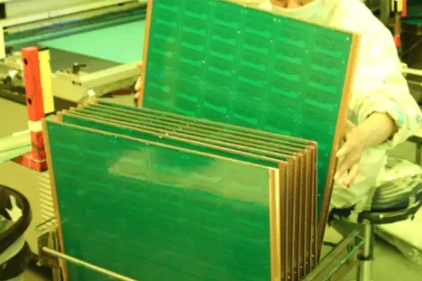
While recently tidying up my studio, I stumbled upon a stack of comparison photos showing circuit board prototypes side-by-side with their mass-produced counterparts. Looking at these boards, I suddenly realized that many people might not fully grasp what the differences between a PCB prototype and a mass-produced unit actually entail.
The prototyping process is actually quite fascinating. Receiving samples of a new design feels a bit like opening a “mystery box”—filled with both eager anticipation and a touch of nervousness. I recall one instance where, in an effort to validate a specific interface design, I had to iterate through three separate prototype runs before finally getting it right; each time required a complete readjustment of the board layout. Such iterative revision is utterly inconceivable during large-scale manufacturing, as a production line simply cannot be brought to a halt to wait around for the sake of a single project.
Flying probe testing proves particularly useful during the prototyping phase. It requires no specialized test fixtures; a few probes moving back and forth across the board are sufficient to complete basic connectivity checks. Although it cannot match the speed of the dedicated testing equipment used in mass production, it is more than adequate for validating the underlying design concepts.
Once you truly transition into the mass production phase, you’ll discover that your entire mindset must shift. The prototyping phase focuses on the question: “Can this design be realized?” Mass production, however, demands that you consider: “Can this design be manufactured reliably—a thousand times over, or even ten thousand?” I once worked on a project where the prototypes performed flawlessly; yet, when we reached mass production, supply fluctuations regarding a single component forced us to recalibrate parameters across the entire assembly line.
The distinction between prototypes and mass-produced units is not merely a difference in quantity; it represents a fundamental difference in mindset. During prototyping, you have the freedom to let your imagination run wild and experiment with various solutions. In the mass production phase, however, every single detail must undergo rigorous scrutiny—because any minor issue, when multiplied by the sheer volume of units, can quickly escalate into a major catastrophe.
Working with circuit boards is a rather interesting endeavor. When you first start out making prototypes, your primary objective is speed—you just want to get it up and running. You aren’t overly particular about whether the soldering is absolutely perfect or if the components are perfectly aligned; after all, it’s just a handful of boards that can easily be handled manually. At this stage, your sole concerns are whether the indicator lights turn on and whether the program executes correctly. You simply don’t have the time—or the means—to meticulously inspect for minute soldering defects, such as voids beneath a BGA package or cold solder joints.
But when it comes time to enter true mass production—well, that’s an entirely different ballgame. You have to consider how to guarantee the reliability of every single board when you’re dealing with thousands upon thousands of them. This is where automated machinery becomes indispensable. In-Circuit Testing (ICT), for instance—an “in-line” testing method—can simultaneously probe a multitude of test points at lightning speed. However, you shouldn’t expect it to catch absolutely everything; it serves primarily as a static inspector. For dynamic performance—how the board behaves while operational—you’ll need to rely on other diagnostic methods.
My primary focus is on how to intercept issues at the earliest possible stage, rather than waiting until the very end to hunt for defects. Take Automated X-ray Inspection (AXI), for example: it’s like giving the circuit board a CT scan. It provides crystal-clear visibility into the quality—good or bad—of solder joints hidden beneath components. This is especially critical now that 3D AXI has become the standard; it can even detect voids within the solder itself—a capability of immense importance for ensuring long-term product reliability.
The entire mindset must shift as you transition from the prototyping phase to mass production. The former is about trial and error; the latter is about error prevention. During the prototyping stage, you can tolerate a certain failure rate—after all, the quantities are small, and adjustments can be made quickly. However, in mass production, a single oversight can trigger massive rework requirements, resulting in staggering financial losses. Therefore, the true test of one’s expertise lies in anticipating every conceivable scenario during the design phase and validating them proactively through various means—rather than waiting until the boards have already been manufactured to attempt a belated “fix.” By then, the cost of remediation is simply too high.
Ultimately, prototyping is about exploration, whereas mass production is about commitment. The former permits the unexpected; the latter demands absolute predictability. Navigating this fundamental transition is, without a doubt, the most challenging aspect of the entire process.
Working with circuit boards is a fascinating endeavor. When I first started out making prototypes, I felt as though I had it all figured out—wasn’t it simply a matter of drawing up the schematics and sending them off to a fabrication house? However, the moment I held the physical board in my hands for the very first time, I realized just how wrong I was.
I recall one particular board where, in an effort to conserve space, I placed several components far too close together. The prototype looked absolutely flawless on the surface; yet, once we moved into mass production, problems immediately arose. The automated pick-and-place machines simply couldn’t position the components accurately. We were ultimately forced to redesign the board—a setback that cost us a full two weeks of delay. That experience taught me a valuable lesson: the so-called “perfection” observed during the prototyping stage often conceals a multitude of hidden pitfalls.
It wasn’t until we truly embarked on mass production that I realized my previous “small-scale” experiences were woefully inadequate. One of the veteran technicians on the production line offered a particularly vivid analogy: “Prototyping is like embroidery; mass production is like weaving.” The former is about meticulous, fine-grained craftsmanship; the latter is about rhythm and flow. On an assembly line, the seamless coordination of every single stage is far more critical than simply ensuring that any one individual board looks aesthetically pleasing. When it comes to process differences, the most obvious distinction lies in the etching stage: prototype shops can fine-tune the chemical solutions on the fly, whereas mass production lines must maintain a fixed concentration. Sometimes, for the sake of efficiency, one is forced to sacrifice a bit of precision; in such cases, the shortfall must be compensated for through design and material choices—for instance, by selecting a more stable substrate or by widening the spacing between circuit traces.
The biggest headache arises when dealing with boards that require special processing. I recall an instance where a client insisted on using a specific imported ink; however, during mass production, we discovered it was completely incompatible with high-speed printing equipment. Ultimately, we had to make a last-minute switch to a similar domestic product. This entire adaptation process—transitioning from prototyping to mass production—truly requires a continuous cycle of trial and error.
Nowadays, whenever I see newcomers excitedly poring over their first prototype boards, I am reminded of all the pitfalls I stumbled into myself. In reality, the most critical requirement for the journey from prototype to mass production is not the pursuit of perfection, but rather the ability to strike a balance between the ideal and the practical. That is the true test of an engineer’s competence.
When it comes to circuit board manufacturing, prototyping and mass production are, in fact, two entirely different beasts. Many people assume that prototyping is merely small-scale production; however, holding this view makes one highly susceptible to costly errors. I made this very mistake myself when I first ventured into hardware design, and it wasn’t until I had suffered a few setbacks that the reality finally sank in.
I recall one instance where a prototype board performed flawlessly, only to encounter issues the moment we transitioned to the mass production phase. We eventually discovered that the package of a specific component—which posed no problem when hand-soldered during prototyping—could not be reliably gripped by the automated pick-and-place machines used in mass production. This is a textbook example of failing to consider DFM (Design for Manufacturability)—designing solely with functional implementation in mind, without regard for the manufacturing process.
Prototyping serves primarily as a means to validate whether a concept is functionally viable. During this stage, you can boldly experiment with various approaches. For instance, in a recent project of mine, I went through three different layout iterations during the prototyping phase before finally settling on the most optimal configuration.
However, once you enter the mass production phase, you must shift your mindset. The focus then shifts to maximizing production line efficiency while minimizing costs. A practical example illustrates this point: we once designed a board that passed every test perfectly during prototyping; yet, during mass production, we discovered that a specific capacitor was positioned too close to a connector. Consequently, an extra few seconds had to be added to the assembly time for every single board just to adjust the pick-and-place sequence.
DFM is not merely a checklist to be reviewed after the design is complete; rather, the feasibility of manufacturing must be taken into account from the very moment you draw the first trace. The habit I have cultivated is this: whenever I finish laying out a specific module, I immediately ask myself, “Is this layout conducive to efficient operation on an automated pick-and-place machine?” Are the test points easily accessible to probes? Such details may seem trivial.
A truly professional team will simulate mass-production conditions right from the prototyping stage. For instance, we deliberately select the exact same PCB substrate materials used in mass production.
The transition from prototyping to mass production is akin to moving from the laboratory to the marketplace. This process demands that designers possess a genuine understanding of how the production line operates. Nowadays, whenever I review a design, I ask myself: Will this design create complications for the manufacturing department during large-scale production?
Ultimately, success in hardware innovation often comes down to more than just whose design looks the coolest.
I have seen far too many teams make the same mistake during the PCB development process: they treat prototyping as if it were merely a small-batch production run. In reality, these are two entirely different things. The core value of prototyping lies in validating the feasibility of a design, not in striving for absolute perfection. I recall one team that, in pursuit of a flawless prototype, spent two whole months repeatedly tweaking their design—only to encounter unexpected thermal dissipation issues once they finally reached mass production.
What truly matters is fully exposing potential issues during the prototyping phase. On one occasion, we designed a board that performed flawlessly in simulation software; however, when the physical prototype was produced, we discovered severe interference affecting the high-frequency signals. Had we not conducted physical testing, this problem might have gone undetected until customer complaints started rolling in. The lead times for prototypes are typically quite short; paradoxically, this compels the team to make rapid decisions rather than getting bogged down in an endless loop of optimization.
Once the process reaches the mass production stage, the entire logic shifts completely. The focus at this point turns to stability and consistency. I once worked on a project where a last-minute change in the supplier for a single component during mass production resulted in compatibility issues across the entire batch of products. This lesson taught me a profound truth: design changes should be avoided as much as possible during the mass production phase—because every single modification has the potential to trigger a chain reaction.
The nature of testing also changes significantly. During the prototyping phase, we might only need to verify basic functionality; however, testing during mass production must cover a wide range of extreme conditions. We once overlooked the impact of temperature and humidity on a specific chip, which subsequently led to widespread product failures in the southern market. Such issues are difficult to detect during the prototyping phase because the testing conditions are typically much more lenient.
The ideal approach is to manage prototyping and mass production as two distinct, independent processes. During the prototyping phase, one should be bold enough to experiment with various solutions—even if some ideas appear somewhat unpolished. Conversely, once the transition to mass production occurs, attention must be focused squarely on process control and supply chain management. The transition between these two phases requires clearly defined milestones, rather than a vague, nebulous handover. Some engineers are always tempted to solve every problem all at once; however, in practice, a better approach is to tackle issues in stages. During the prototyping phase, the primary focus should be on technical feasibility, reserving cost and efficiency optimization for the mass production stage. This division of labor allows the team to remain more focused and makes it easier to achieve substantive progress at each specific stage.
When it comes to circuit board manufacturing—having personally experienced the entire journey from prototyping to small-batch production—I’ve noticed that many people tend to overlook a critical point: the differences between a PCB prototype and mass production are not merely a matter of quantity; rather, they represent a fundamental shift in the entire production logic.
During the prototyping phase, our focus tends to be heavily centered on functional verification, and we are relatively less sensitive to cost considerations. I recall one instance where, in order to test a specific impedance requirement, we insisted on proceeding with a particular design—even though we knew full well it would incur additional expenses—simply because we were only producing a handful of sample boards. However, once we transitioned into the small-batch production phase, we discovered that those “additional costs” which had seemed perfectly acceptable during prototyping were now multiplying exponentially.
I had a particularly profound realization regarding the selection of PCB substrate materials. During the prototyping phase, we typically use standard FR-4 material; however, when scaling up to a small batch of 50 boards, our supplier recommended switching to a more cost-effective alternative. This single adjustment alone resulted in significant cost savings. While such a modification might seem negligible in the context of large-scale mass production, for small-batch runs, it constitutes a tangible and substantial cost optimization.
A veteran technician on the production line once told me that, when dealing with small-batch manufacturing, the biggest headache is frequent line changeovers. They would much rather take on a month-long continuous order than have to switch between different board specifications every single day. This made me realize that the practical realities of the production floor must be taken into account right from the design stage. For instance, striving to standardize board thickness and minimizing requirements for specialized processes—these seemingly minor design decisions can have a direct impact on the final quotation.
I recently assisted a friend’s company with a project where they originally intended to produce 200 boards featuring blind and buried vias. I suggested a slight adjustment to the design, replacing some of the blind/buried via structures with standard through-holes. Although this increased the board thickness by 0.2 millimeters, the overall cost dropped by nearly 30%. This kind of trade-off is particularly crucial in small-batch production, as the surcharges associated with specialized processes can become prohibitively high as production volume increases.
In reality, the most significant shift required when transitioning from prototyping to small-batch production is a change in mindset. During the prototyping phase, one can pursue peak performance without compromise; however, for small-batch production, one must begin to balance manufacturability with economic viability. It is akin to the difference between a bespoke suit and ready-to-wear clothing: the former allows for the pursuit of a perfect fit regardless of cost, while the latter requires finding the optimal solution within the constraints of standard sizing.
I have now cultivated a habit: after completing functional verification, I invariably invite production engineers to review the design with me. They are consistently able to offer suggestions for improvement from a manufacturing perspective—such as adjusting routing density to ensure more uniform etching, or optimizing the panelization layout to maximize material utilization. These insights, born of practical experience, often prove far more effective than any standard design guidelines.
Ultimately, the essence of the transition from PCB prototyping to mass production lies in shifting from a technology-centric approach to a business-centric one. A successful product requires not only robust functionality but also a reasonable manufacturing cost. This is especially true for small-batch projects; how effectively this transitional phase is managed directly determines whether the product can successfully make the leap from the laboratory to the marketplace.
I still vividly recall the thrill I felt the first time I held a sample of a circuit board I had designed myself. Back then—having just learned the basics of schematic capture—I was eager to rush my designs to a prototyping house to fabricate test boards, which I would then debug to verify the validity and feasibility of my concepts. The result? While the functionality was successfully realized, the cost was shockingly high—hardly surprising, given that I was producing only a handful of boards at a time! It was only later, as I gained exposure to a wider range of projects, that I came to understand that the distinction between PCB prototyping and mass production involves far more than just a simple difference in quantity. The etching process tends to be somewhat more flexible during the prototyping phase; since the volume is low, engineers might manually tweak parameters to achieve specific aesthetic or functional details—such as line precision or surface finish quality. However, once mass production begins, the machines churn out thousands upon thousands of units; consequently, every single parameter must be locked down rigidly beforehand. Otherwise, a tiny deviation at the start can lead to catastrophic errors down the line! I once worked on a project where we overlooked this critical point, resulting in the entire first batch of mass-produced goods being scrapped—a devastating financial loss.
Let’s further explore the differences between prototyping and mass production. Prototyping is akin to conducting experiments in a laboratory; it offers ample room for trial and error, allowing for iterative design revisions until the desired result is achieved. Mass production, conversely, resembles a factory assembly line, prioritizing maximum stability and efficiency. Attempting to alter the design at that stage? The associated costs would be astronomical! For this reason, many companies opt for a small-batch pilot run first to validate the maturity of their manufacturing processes before scaling up to full-volume production.
The lamination process follows a similar logic. During prototyping, a small-scale press might be used to process just a few boards at a time, making it relatively easy to control temperature and pressure. However, when switching to a large-scale, multi-opening press for mass production, the uniformity of heat distribution becomes a critical challenge—otherwise, some boards might end up with uncured adhesive while others are completely scorched! This necessitates extensive upfront simulation modeling and physical testing by engineers to ensure a foolproof outcome.
In my view, the most difficult aspect of the transition from prototyping to mass production is not the technology itself, but rather the required shift in mindset. During prototyping, our primary focus is simply: “Can we actually build this?” During mass production, however, the focus shifts to: “How can we build this quickly, cost-effectively, and consistently?” This demands that engineers possess expertise not only in design but also in materials science, equipment operation, and even supply chain management; otherwise, even the most brilliant concept could stall out during the final stretch of implementation.
Looking back now, the pitfalls we encountered have actually become invaluable learning experiences. At the very least, they taught me that there are no shortcuts in the electronics manufacturing industry; only by thoroughly mastering every single stage of the process can one produce truly reliable products.
When it comes to manufacturing circuit boards, I’ve seen far too many people treat the prototyping phase as if it were merely a small-batch production run—a mindset that sets them off on the wrong track right from the start.
I recall helping a friend with a smart home project last year; during the prototyping phase, they became fixated on ensuring that every single solder pad was perfectly symmetrical, leading them to go through seven or eight design revisions. In reality, the primary focus at that stage should have been on validating whether the circuit’s functionality met the required specifications—not on obsessing over manufacturing process details that are only relevant once mass production begins. For instance, one might use flying leads to temporarily bridge key signal points for functional verification, or employ adjustable resistors to assess the impact of varying parameters on circuit performance. These temporary adjustment techniques are invaluable during the prototyping phase, enabling rapid validation of design hypotheses.
The essence of prototyping lies in validating design concepts—much like a painter first sketches a rough draft. It is my habit during the initial prototyping run to deliberately leave several optional component footprints open, allowing for flexible adjustments during testing. On one occasion, simply by having reserved an extra spot for a capacitor, we successfully resolved a signal interference issue; had this problem gone undetected until the mass production stage, the financial losses would have been substantial. This design flexibility also extends to reserving test points and debugging interfaces to facilitate signal measurement using tools such as oscilloscopes or logic analyzers. Sometimes, I even designate specific “cut zones” on the board to allow for rapid modification of circuit traces during testing.
Once the project truly transitions into the mass production phase, the entire mindset must shift. At this stage, the workers on the assembly line cannot be expected to possess the same intimate knowledge of every minute detail as the design engineers; consequently, the process documentation must be written with the precision of a culinary recipe. For example, it is essential to clearly specify the mounting orientation for each component, as well as the precise soldering duration and temperature parameters; furthermore, one must consider the operational ergonomics and convenience for workers at each station within the assembly line workflow.
I learned a particularly profound lesson from a past project: we had a circuit board where a heat dissipation issue was successfully resolved during the prototyping phase through the skilled manual soldering of a veteran technician. However, when we moved to mass production, the new workers were unable to replicate that same result. We eventually discovered that the soldering temperature profile required precise control—a detail that no one had paid any attention to during the prototyping stage. This experience served as a stark reminder that, even during prototyping, we must simulate mass production conditions—for instance, by utilizing the exact same soldering equipment and process parameters intended for the final mass production run.
Nowadays, I place particular emphasis on meticulous data recording during the transition from prototyping to mass production. Seemingly trivial data points—such as the thermal expansion coefficient of the PCB substrate material—can, in a mass production environment, ultimately determine the overall yield rate of an entire batch of boards. It is also crucial to document the impact of batch-to-batch variations in components on overall performance; such data is indispensable for the subsequent optimization of the manufacturing process.
When discussing the differences between PCB prototyping and mass production, the most significant distinction lies in the underlying mindset. During the prototyping phase, one is free to let their imagination run wild and experiment with a wide array of creative concepts; conversely, during mass production, it becomes imperative to establish a rigorous framework of quality control checkpoints. For instance, prior to commencing mass production, one must formulate detailed inspection standards encompassing various stages, including electrical performance testing, visual inspection, and reliability verification.
A project I am currently working on—an industrial controller—serves as a quintessential example of this dynamic. During the prototyping phase, we experimented with three different solder mask colors to evaluate their thermal dissipation performance; however, for mass production, we will select only the single most optimal solution. This selection process requires a comprehensive assessment of various factors, including thermal performance, cost control, and supply chain stability.
In truth, a skilled engineer should act much like a film director: the prototyping stage serves as the rehearsal—a time when you can call “cut” and start over at any moment—whereas mass production is the live performance, which must be executed flawlessly from start to finish. During the rehearsal phase, the goal is to identify and resolve as many issues as possible—including design flaws, manufacturing challenges, and supply chain risks—before the curtain rises on the main show.
I have come to increasingly feel that striving for absolute perfection during the prototyping stage can actually be a waste of resources. I have seen instances where individuals spent exorbitant sums pursuing “military-grade” standards during prototyping, only to find—once they reached the mass production stage—that they could not find a suitable manufacturer willing to take on the project due to the prohibitively high costs involved. The sensible approach is to select an appropriate prototyping standard based on the product’s specific positioning; after all, the standards required for consumer electronics differ vastly from those required for medical devices.
The truly intelligent strategy is to build a certain degree of flexibility into the prototyping phase, while focusing one’s primary efforts on establishing a robust and reliable manufacturing process. After all, even the most brilliant design ultimately relies on a stable manufacturing process to realize its full value. This entails selecting the right contract manufacturer, establishing a rigorous quality control system, and formulating comprehensive contingency plans for production.
The business of designing and manufacturing circuit boards is actually quite fascinating. When I first started out, I used to think that prototyping and mass production were essentially the same thing—merely a matter of producing a few boards versus producing a large quantity. In reality, however, nothing could be further from the truth.
I have encountered numerous situations where clients were absolutely delighted with their prototype boards, only to run into significant problems once they transitioned to mass production. For instance, we once handled a small-batch order for a medical device using high-frequency PCB laminates. It wasn’t until we were ready to proceed with full-scale production that we discovered the supplier had a strict Minimum Order Quantity (MOQ) requirement. Consequently, the cost of the excess material we were forced to order just to meet that MOQ was entirely amortized across that initial production run, causing the unit price per board to skyrocket overnight.
In fact, when analyzing the differences between PCB prototyping and mass production, the most distinct divergence lies in the way costs are allocated. During the prototyping phase, fixed costs—such as engineering design fees and tooling expenses—must be amortized across a very small batch of boards; naturally, this results in a unit price that appears shockingly high. However, once you transition to mass production, these initial upfront investments can be spread out across thousands or even tens of thousands of boards, significantly lightening the cost burden on each individual unit.
Another point that many people tend to overlook is the potential variation in surface finish processes between the prototyping and mass production stages. During the prototyping phase, manual tinning is often employed; while the results may look excellent, the thermal stress variations encountered on an automated production line can have a significant impact—particularly on certain specialized material combinations. Sometimes, it even becomes necessary to completely overhaul the surface finish strategy to ensure viability.
The most challenging aspect of handling small-batch orders is this awkward “in-between” status: you neither benefit from the cost advantages of large-scale procurement nor avoid the risks associated with material waste. I recall a client who placed an order for just 50 boards; however, due to minimum order quantity requirements for the raw PCB laminates, the actual material utilized amounted to less than one-third of what was purchased. The remainder simply became dead inventory—a pure cost burden.
Consequently, my advice to clients now is this: if you are confident in your product’s direction, plan your initial mass production run with a reasonable quantity. Do not jeopardize the entire project’s cost structure just to save a trivial amount on prototyping fees. After all, during the transition from a few boards to a few hundred, the reduction in unit cost is most pronounced with each additional unit produced; once you cross a certain critical threshold, however, the cost-efficiency gains tend to diminish.
Of course, every project is unique; the key lies in assessing your specific requirements and market expectations. Sometimes, making a slightly higher initial investment can actually pave the way for smoother, large-scale production down the line.
Over my years in the electronics industry, I have observed a particularly interesting phenomenon: many people assume that transitioning from prototyping to mass production is merely a simple process of scaling up. In reality, the underlying logic behind these two modes of operation is fundamentally different.
I remember when we were developing our first smart home controller, the prototyping phase went incredibly smoothly. The prototyping facility delivered five sets of boards to us within just three days, and they passed all our functional tests without a single issue. The team was ecstatic, convinced we were ready to dive straight into mass production.
However, our very first mass production run—an order for 500 boards—proved to be a major stumbling block. During the soldering process, a specific capacitor kept “tombstoning” (standing on end), resulting in a rework rate of 15% and nearly bringing the entire production line to a standstill. We eventually discovered that the design of the solder pads was incompatible with wave soldering—an issue that simply never manifested during the manual soldering used in the prototyping phase.
This illustrates the fundamental difference between prototyping and mass production: the former serves to validate the design concept, while the latter tests the stability and robustness of the manufacturing process.
I now place immense emphasis on the Design for Manufacturability (DFM) review stage. Before releasing any board design for fabrication, I require our engineers to cross-reference every detail against our manufacturing process guidelines. For instance, we verify whether component spacing meets the requirements for automated pick-and-place machines, and whether the solder pad dimensions are compatible with various soldering techniques. These details might seem trivial during the prototyping phase, but in the context of mass production, any minor oversight can quickly escalate into a systemic production failure. On one occasion, in an effort to cut costs, we reduced the PCB thickness from 1.6mm to 1.2mm. The result was widespread board warping during the through-hole component insertion stage; we ultimately had to revert to the original specifications to resolve the issue.
Nowadays, I tend to view prototypes as a form of “stress test”—not merely for verifying functionality, but also for anticipating potential pitfalls that might arise during mass production.
Recently, while developing a wireless module, we deliberately tested three different RF chips during the prototyping phase. Although this incurred slightly higher costs upfront, it allowed us to immediately select the most stable solution for mass production, thereby saving a significant amount of time on debugging later on.
Ultimately, the transition from producing a handful of boards to thousands of boards is a test of the entire supply chain’s collaborative capabilities—it is not merely a matter concerning the production line itself.
On another occasion, to fulfill a rush order, we temporarily switched PCB material suppliers. Although the technical parameters appeared identical on paper, the actual Tg value was lower than specified. This led to delamination issues during the reflow soldering process; had our inline AOI system not detected the anomaly in time, the entire batch of boards would have had to be scrapped.
I have since developed a habit: prior to every mass production run, I set aside two “first-off” samples in my office so that I can readily compare them against the original prototypes whenever necessary.
In truth, what I fear most is that “good enough” mentality—the assumption that simply because a prototype works, the mass-produced version will be trouble-free. The truly reliable approach is to factor in mass production requirements right from the prototyping stage—for instance, ensuring that selected components are readily available for procurement and that the PCB pad layout is compatible with automated assembly processes. Investing a little extra effort in these preliminary stages can spare you a great deal of trouble down the road.
We have recently been experimenting with a new strategy: designing key component footprints to be “compatible” across multiple options. This ensures that even if a specific component model goes out of stock, we can quickly switch to an alternative solution without disrupting production.
At the end of the day, hardware development is an iterative process of encountering and overcoming obstacles. What truly matters is that, with each iteration—whether during prototyping or mass production—we learn something new from the discrepancies we encounter.
Having worked in electronics design for so many years, I have come to realize that many people tend to oversimplify the process of PCB prototyping. Whenever I see someone on the team excitedly holding up a few prototype boards and declaring that the design is “flawless,” I can’t help but feel the urge to temper their enthusiasm with a dose of reality. Prototyping and mass production are two entirely different beasts; the disconnect between these two stages often remains hidden until the moment mass production actually begins.
I recall a project we worked on last year where the performance during the prototyping phase was absolutely flawless. Yet, the moment we transitioned to mass production, problems began to surface—specifically, the impedance matching across the boards went completely haywire. We later discovered that the PCB material supplier had been switched to a cheaper alternative, resulting in unacceptably high fluctuations in the material’s dielectric constant. Issues of this nature are virtually impossible to detect during the prototyping phase, simply because prototype manufacturers invariably utilize top-tier materials.
Nowadays, I place a particularly strong emphasis on supplier selection during the prototyping stage. Many people assume that finding just any cheap vendor will suffice—after all, they reason, you’re only making a handful of boards. However, my experience tells me that it is absolutely essential to partner with manufacturers capable of accurately simulating mass-production processes. For instance: Can etching precision be maintained consistently? Will there be any deviations in solder mask thickness? These minute details ultimately determine whether your design can successfully transition into mass production.
On one occasion, in a rush to meet a tight deadline, we simply scoured Taobao to find the cheapest prototyping service available. While they did indeed produce the prototypes quite quickly, we discovered during the mass-production phase that their process parameters diverged drastically from those of our chosen contract manufacturer. The sheer effort required to recalibrate the production line alone cost us a two-week delay—a financial loss that, no matter how you calculate it, was simply massive.
Speaking of the differences between PCB prototyping and mass production, I believe the most easily overlooked aspect is the testing phase. During prototyping, testing might be limited to a simple continuity check, or at most, a basic functional test. However, for mass production, you must consider whether your test coverage meets the required standards and whether the testing duration can be kept within a reasonable timeframe. All of these factors need to be planned for as early as the prototyping stage.
Whenever I embark on a new project now, I make a point of specifically requesting a comprehensive process report from the prototyping manufacturer. While the data contained within these reports may appear dry and tedious, it serves as an invaluable tool for predicting potential issues that might arise during mass production. For example: How uniform is the copper thickness? Does the quality of the plated through-hole walls meet the required specifications? These seemingly subtle discrepancies often prove to be the deciding factors in the ultimate success or failure of a mass-production run.
Ultimately, the true purpose of prototyping should not merely be to validate the correctness of the circuit design itself, but—more importantly—to verify that your design can be manufactured reliably and consistently. Embracing this shift in perspective is crucial, as it enables you to sidestep numerous pitfalls associated with mass production right from the very early stages of development.
A relay control board that works perfectly in the lab can fail
A medical pump PCB that performs flawlessly in the lab can produce
The ADAS controller PCB is no longer a passive substrate — it
- 중소규모 배치 생산 전문가
- 고정밀 PCB 제작 및 자동화된 조립
- OEM/ODM 전자 프로젝트를 위한 신뢰할 수 있는 파트너
영업 시간: (월~토) 9:00~18:30