
Industrial Automation PCB Reliability: How to Achieve 10+ Years of Stable Operation
In the field of industrial automation, people often pay attention to AI
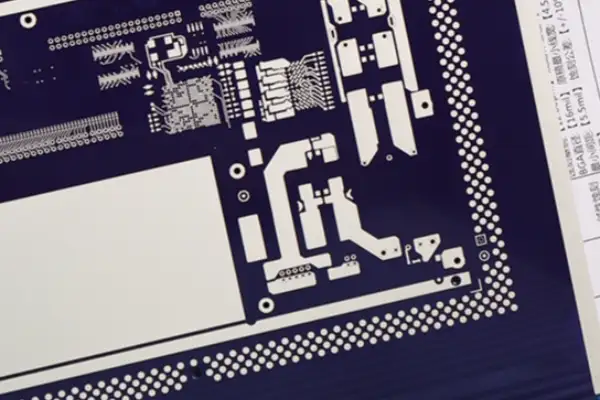
I have always found working in the telecommunications equipment sector to be fascinating. Many people might assume that a PCB is nothing more than a simple green circuit board; in reality, however, it carries the very lifeblood of the entire communication system. For instance, in 5G base station equipment, a single palm-sized PCB might integrate thousands of components; any deviation in even a single signal path could lead to a degradation in the entire system’s performance. This level of precision is akin to building a miniature city on the surface of a fingernail, where the width and spacing of every “street” must be accurate to the micron level.
I recall an instance where we encountered a particularly thorny problem: severe attenuation of high-frequency signals. At the time, some members of the team suggested switching materials, while others proposed redesigning the layout; ultimately, however, we discovered that the root cause lay in impedance matching. This experience made me realize that, sometimes, the most fundamental aspects are actually the most critical. Specifically, measurements taken using a Time-Domain Reflectometer (TDR) revealed that deviations in the calculated width of the transmission lines caused signal reflections whenever the signal encountered a sudden impedance mismatch. These reflected waves then superimposed upon the incident waves, ultimately resulting in compromised signal integrity. Resolving this issue required recalculating the characteristic impedance of the transmission lines and adjusting the ratio between the line width and the dielectric thickness.
The telecommunications industry places demands on reliability that border on the exacting. I have witnessed situations where an entire batch of equipment had to be reworked due to a single, minuscule soldering defect. The resulting loss was not merely financial; it represented a significant waste of time and resources. For example, during the wave soldering process, if the flux activity is insufficient or the preheating temperature is inappropriate, “cold solder joints” may form. Such defects might not immediately manifest during initial testing, but after the equipment has been in operation for an extended period, they can lead to poor electrical contact and, ultimately, total system failure. Many manufacturers today are striving to achieve higher operating frequencies in their applications; however, this pursuit demands the support of increasingly precise manufacturing processes. For instance, micro-via technology can effectively boost routing density, yet it simultaneously increases manufacturing complexity. Taking millimeter-wave band applications as an example: once signal frequencies reach 28 GHz, the precision offered by traditional mechanical drilling is no longer sufficient to meet requirements. Consequently, laser drilling technology—a process that imposes specific demands on the substrate’s coefficient of thermal expansion and glass transition temperature—becomes indispensable.
The testing phase is often the most easily overlooked aspect of the process. Many assume that if the design is sound, everything else will fall into place; in reality, however, testing serves as the true touchstone for verifying a product’s reliability. In practice, we must go beyond standard room-temperature testing to simulate extreme environmental conditions—for instance, by monitoring device performance fluctuations during thermal cycling tests ranging from -40°C to +85°C. Such rigorous testing protocols frequently uncover issues that were difficult to anticipate during the initial design phase.
I particularly admire an approach that integrates testing throughout the entire development lifecycle—specifically, by prioritizing “testability” right from the design stage—as this can prevent a great deal of trouble down the road. For example, designating specific test points during the layout phase or considering the ease of probe contact when selecting component packages may seem like trivial details; however, during the mass production phase, these small considerations can significantly boost testing efficiency.
When it comes to material selection, it is undeniably a process that requires careful trade-offs. High-performance materials often come with a higher price tag; finding the optimal balance between performance and cost is a challenge that puts every engineer’s judgment to the test. Consider PTFE-based substrates, commonly used in high-frequency circuits: while they boast exceptional dielectric constant stability, their cost can be more than ten times that of standard FR-4 materials. Consequently, material selection must be carefully tailored to the specific requirements of each application scenario.
I have recently observed a growing trend toward the adoption of “hybrid lamination” processes. This approach—which simultaneously ensures high performance in critical areas while keeping overall costs in check—is indeed a clever strategy. For instance, one might utilize Rogers 4350B material in the RF section while continuing to use conventional FR-4 for the digital circuitry. By bonding these disparate core materials together through a lamination process, this hybrid structure not only preserves signal integrity but also avoids the significant cost burden associated with using premium-priced materials across the entire board.
Ultimately, the greatest joy in this profession lies in the continuous process of solving new problems; the sense of accomplishment derived from overcoming technical bottlenecks is a reward that few other jobs can offer. Of course, the pressure is also immense; after all, communication equipment directly impacts the network quality experienced by countless households, leaving absolutely no room for negligence. I remember one instance where, in an effort to meet a specific phase noise specification, our team worked continuously for 72 hours straight. When the final test results finally met the target, the sense of elation was truly indescribable.
Sometimes, while debugging equipment late at night—gazing at the stable waveforms displayed on the oscilloscope—I feel that every bit of effort has been worth it. This profound sense of fulfillment is likely the driving force that sustains us and keeps us moving forward. This feeling is particularly strong after completing the debugging of a new base station unit; knowing that hundreds of thousands of users will soon enjoy high-speed network access through this very equipment makes me feel that the significance of this work extends far beyond the technology itself.
I’ve always felt that selecting materials for communication circuit boards is a bit like choosing a pair of shoes—only your feet can truly tell if they fit. Last year, our team encountered a rather interesting situation: a client insisted on using a specific imported substrate—touted as having “perfect” specifications—for their 5G base station antenna boards. However, when the prototypes were tested, we discovered that the signal attenuation was 15% higher than expected. After extensive troubleshooting, we finally pinpointed the problem: the material’s dielectric constant (Dk) fluctuated too drastically with changes in temperature.
This incident taught me a valuable lesson: the “ideal parameters” listed in a datasheet are an entirely different matter from how a material actually performs in a real-world application. For instance, some manufacturers like to boast about how impressive their ultra-low dielectric constant values look on paper; yet, in a field environment, temperature swings can be extreme—plummeting from minus 20 degrees Celsius to soaring up to 70 degrees. In such scenarios, the critical factor is the *stability* of the Dk value, not merely its absolute magnitude. In fact, during high-frequency signal transmission, even a minute drift in the dielectric constant can lead to phase distortion—a particularly critical issue for Massive MIMO systems utilizing large-scale antenna arrays, where such distortion directly compromises the precision of beamforming. We subsequently used a Vector Network Analyzer to scan the material across various temperature gradients; the results revealed that the Dk value began to exhibit nonlinear, abrupt shifts once the temperature reached 40°C—precisely the most sensitive operating range for the millimeter-wave frequency band.
I also recall a visit to a manufacturing plant to observe a mass production run; the workers were grappling with lamination defects caused by a mismatch in the coefficients of thermal expansion (CTE). At the time, an engineer pointed to an X-ray image and explained to me that the shrinkage rates of the two materials differed by just a few parts per million (ppm); during the high-temperature reflow soldering process, this discrepancy created a tension akin to two people pulling a piece of fabric in opposite directions. We eventually resolved the issue by adjusting the resin formulation to flatten out the CTE curve. This case underscored for me that material compatibility must be evaluated at a molecular level—specifically, that a dynamic equilibrium must be achieved between the cross-linking density of the epoxy resin and the shrinkage ratios of the glass fabric along its warp and weft axes. One supplier, by introducing nanoscale silicon microsphere fillers, successfully managed to keep the Z-axis coefficient of thermal expansion (CTE) within 40 ppm/°C. Such optimization of microstructure is often far more critical than the manipulation of macroscopic parameters.
Nowadays, whenever I review a report on new materials, I invariably ask a follow-up question: Under what specific conditions were these data obtained? A dielectric constant (Dk) value derived in a laboratory’s temperature- and humidity-controlled environment might turn out to be a completely different story when the material is deployed on a base station tower. After all, telecommunications equipment must operate continuously for over a decade—enduring everything from torrential downpours to scorching sunlight—so the materials used must truly stand the test of time. We have established an environmental simulation chamber capable of replicating extreme scenarios, such as the salt-laden mist of coastal regions or the dry heat of deserts. We once tested a material that, after 2,000 hours of exposure to 85°C and 85% relative humidity, saw its dielectric loss surge threefold; such accelerated aging tests offer far more practical insight than any promotional brochure ever could.
While recently testing a domestic composite material, we observed an intriguing phenomenon: although its initial dielectric constant was 0.2 points higher than that of its imported counterparts, it actually demonstrated superior stability after undergoing a 2,000-hour aging test. This reminded me of something my physics teacher once said: sometimes, taking things a little slower actually leads to a more stable and reliable outcome. A deeper analysis revealed that the material’s multilayer woven ceramic fiber structure creates a stress-buffering mechanism; during drastic temperature fluctuations, these heterogeneous interfaces effectively dissipate thermal stress—much in the same way that steel reinforcement works synergistically within concrete. Conversely, certain materials that prioritize achieving extreme initial performance often rely on a monolithic crystalline structure, which ironically makes them prone to developing lattice defects during prolonged thermal cycling.
In reality, the greatest pitfall in designing PCBs for telecommunications is the blind pursuit of being the “champion” in a single specific metric. I have witnessed far too many cases where, in an attempt to push the loss factor down to its absolute limit, the manufacturing yield plummeted to below 30%; or where, in the quest for an ultra-low Dk value, a specialized filler was selected that resulted in severe edge chipping during the drilling process. The true test of an engineer’s expertise lies in their ability to strike a proper balance across all performance metrics. For instance, for the millimeter-wave radar boards we are currently developing, we have established a weighted scoring system encompassing twelve distinct parameters—including dielectric thickness tolerance, surface roughness, and copper foil elongation. Although one particular material from a Finnish manufacturer ranked only fifth in terms of its Dk value, it ultimately achieved the highest overall score—a testament to the power of systematic, holistic thinking.
Ultimately, the selection of materials is less of a simple “true or false” question, and much more of a complex multiple-choice problem. Whenever we design a new circuit board, we take our candidate materials and fabricate them into test boards, subjecting them to three months of accelerated aging. Observing the resulting impedance variation curves—rather than simply poring over data sheets—proves to be a far more convincing approach. After all, a telecommunications base station isn’t a laboratory exhibit; it must be capable of withstanding the wind, rain, and frost of the real world. Recently, we’ve even begun incorporating AI algorithms to build predictive models for material defects by analyzing historical failure cases. This data-driven selection method is fundamentally transforming our traditional, experience-based decision-making processes.
I’ve always found the subject of circuit board manufacturing within the telecom industry to be quite fascinating. Many people might assume this line of work is merely a matter of pitting parameters against specifications—but in reality, that couldn’t be further from the truth. I’ve seen far too many engineers pour all their energy into material selection—and while materials are undoubtedly important—they often overlook the seemingly insignificant details embedded within the broader manufacturing process. Take a recent project of ours, for instance: despite utilizing top-tier high-frequency laminate materials, we still encountered signal attenuation issues. We later discovered the culprit was simply an improperly calibrated temperature profile during the lamination process.
Telecom equipment places exceptionally high demands on circuit board stability; after all, a base station is a piece of hardware that, once installed, is expected to remain in service for many years. Sometimes, even a minor deviation in the manufacturing process can necessitate the rework of an entire batch of boards. I recall visiting a factory on one occasion and observing their “hybrid lamination” process; the fact that they had to precisely control even the humidity levels within the workshop left a lasting impression on me. While many manufacturers today are chasing breakthroughs in novel materials, I believe that refining and perfecting the fundamental manufacturing processes yields far more tangible and practical results.
The issue of signal integrity cannot be resolved solely through the use of simulation software. Actual production environments are rife with variables; for instance, even slight non-uniformity in copper plating thickness can compromise impedance control. During one testing phase, we discovered that high-frequency signals were suddenly degrading within a specific frequency band. After extensive troubleshooting, we traced the problem back to fluctuations in the thickness of the immersion gold plating. Such issues are completely invisible on engineering schematics; only engineers with a deep, practical understanding of manufacturing processes can identify them.
I’ve come to increasingly realize that a truly excellent circuit board is the product of a collaborative synergy—a process of mutual adjustment and refinement—between the design team and the manufacturing team. Designers cannot afford to exist solely within the realm of idealized theoretical models; they must possess a firm grasp of the factory’s actual processing capabilities. Conversely, manufacturers cannot blindly adhere to standard operating procedures; they must strive to comprehend the underlying electrical requirements that drive the design. Just the other day, I learned of a project where poor communication between the two parties resulted in the circuit board undergoing five separate revisions before finally meeting specifications—a wasteful expenditure of resources that was truly regrettable.
Ultimately, given the rapid pace of technological iteration within the telecom industry, focusing exclusively on material performance metrics can actually cause one to lose sight of the broader strategic direction. True competitiveness lies in meticulously perfecting every single detail—forming a complete closed loop that spans everything from material properties and manufacturing processes to quality inspection. Behind those base stations that operate stably over the long term, there is often a rigorous manufacturing system providing support, rather than merely a breakthrough in a single specific technology.
While recently discussing a new project with our suppliers, I noticed they have begun integrating process control data directly into our design-side database—an excellent approach. This collaborative model allows designers to view, in real-time, the yield rate for specific trace widths during actual production; it is precisely this kind of synergy that truly enhances the reliability of circuit boards.
After all, telecommunications equipment must be capable of withstanding the elements—wind, sun, and rain—and these circuit boards serve as the cardiovascular system of the entire network.
Having spent years designing PCBs for the telecommunications sector, I have come to a profound realization: many people tend to get fixated on technical parameters right from the start. In reality, those figures written down on paper represent nothing more than the basic entry threshold.
I have encountered far too many engineers who treat IPC standards as if they were gospel, memorizing them verbatim. For instance, on one occasion, a client became obsessively fixated on an impedance deviation of just a few micrometers—a dispute that ultimately delayed the project schedule by two weeks—only for the final product to show absolutely no measurable difference in performance when tested in a real-world environment.
Conversely, the factors that truly impact communication quality are often those easily overlooked details. Take power distribution, for example: we once designed a base station board where every parameter met the required specifications, yet the high-frequency signals remained unstable. We eventually discovered that the issue stemmed from uneven copper foil thickness in a specific corner of the power plane, which prevented the instantaneous current from keeping pace with demand.
Thermal management is another major pitfall. We once designed a router PCB that performed flawlessly in the laboratory; however, after operating continuously for just a few hours in the field, it began dropping data packets. Upon disassembly, we discovered that the placement of the ventilation holes was obstructing the airflow path to a critical chip.
When it comes to designing telecommunications PCBs, I prioritize overall system synergy over the sheer perfection of any single isolated metric. For instance, if you push trace widths to their absolute physical limits in pursuit of extreme impedance precision, only to see your manufacturing yield plummet by half, the trade-off is clearly not worth it.
I generally treat data points such as “solder stub length” merely as reference values. In actual production, different batches of PCB laminate materials from various suppliers will inevitably exhibit subtle variations; rigidly adhering to a single specific number can, ironically, make you more prone to failure.
I have now adopted a mindset where I treat the circuit board as a living organism. The technical standards serve as the skeletal structure, but what truly ensures the equipment operates with stability and resilience is the holistic layout—the intricate network of interconnections that functions as its lifeblood. Sometimes, slightly relaxing the tolerance in one specific area—thereby freeing up that “precision budget”—and reallocating it to more critical aspects, such as signal isolation, can actually yield far superior results.
A recent 5G small-cell base station project I worked on serves as a prime example. On the surface, the impedance control didn’t appear flawless; however, by optimizing power supply filtering and component partitioning, our measured bit error rate proved to be even lower than that of competitors who rigidly adhered to every single parameter specification. Designing PCBs is much like cooking: simply measuring out spices with absolute precision doesn’t guarantee a delicious meal; you must also master the “heat” and the interplay of ingredients.
Ultimately, design standards serve merely as tools to help you avoid obvious errors. A truly exceptional PCB design relies on a deep understanding of the subtle, underlying relationships—such as current flow paths and electromagnetic compatibility.
While recently researching high-frequency PCB design, I observed that many engineers focus excessively on a material’s dielectric constant while overlooking the actual impact that routing topology has on signal quality. I once encountered a perplexing issue while debugging a communication module: despite having selected top-tier high-frequency laminate materials, the signal exhibited inexplicable jitter.
After extensive troubleshooting, I discovered that the root cause lay in the stripline design. In an effort to conserve board real estate, I had routed several critical signal lines on the inner layers; I initially assumed this would provide superior shielding, but the result was actually the opposite—coupling between adjacent layers led to significant signal integrity issues.
I was particularly struck by an incident involving a design flaw in a high-speed interface. Because we failed to adequately account for the impact of via stubs, the rising edge of the signal suffered severe distortion; ultimately, we were forced to completely redesign the board to resolve the issue.
Impedance matching is a concept that is simple to articulate but difficult to execute—particularly in multi-layer PCB designs, where traces on different layers often require distinct calculation models. I’ve noticed that a common mistake among novice engineers is to blindly apply textbook formulas without accounting for the specific characteristics of the actual laminate materials or the inherent variances introduced by the manufacturing process.
I recall visiting the factory of a telecommunications equipment manufacturer on one occasion, where their engineers showed me a fascinating case study: to control impedance fluctuations in critical signals, they went so far as to adjust the concentration parameters of the etching solution. This made me realize that every single detail in the PCB manufacturing process can potentially impact the final impedance accuracy.
My deepest realization in high-frequency circuit design is that theoretical calculations are merely a starting point; true optimization requires continuous adjustment based on actual measurements. For instance, when I was designing a microwave transmission module some time ago, the parameters generated by the simulation software consistently deviated from the results obtained during physical testing. Ultimately, it was through a process of repeated trial and error that we discovered the optimal solution.
Nowadays, whenever I design a new telecommunications circuit board, I pay particular attention to the geometry of the transmission lines; sometimes, a fine-tuning of just a few microns in line width can yield a significant improvement in performance. Although this process of minute adjustment can be tedious, seeing the final, stable signal waveforms makes it all feel entirely worthwhile.
In truth, the longer one works in this field, the more one comes to appreciate the artistry inherent in high-frequency circuit design. It involves more than simply adhering to technical specifications; it demands the ability to exercise flexible judgment based on the specific application scenario. For example, when addressing the issue of “stubs”—unwanted remnants of transmission lines—one must carefully weigh the trade-offs between manufacturing costs and performance requirements to identify the most suitable balance point.
I’ve recently been pondering a specific subject: the PCB boards tucked away inside telecommunications equipment—particularly those sections directly related to power supply management. Many people tend to jump straight into discussing technical parameters and specifications, but I believe that what truly determines whether a board can withstand the rigors of a real-world operating environment are often those subtle details that are easily overlooked.
For instance, I once dismantled a piece of equipment from an old base station and noticed that the power traces on its telecommunications PCBs were laid out in a particularly intriguing manner. Instead of following a rigid, rectilinear pattern, they branched out in a fashion reminiscent of tree limbs. A veteran engineer explained to me that this design serves to distribute the current load—a concept rooted in a simple, pragmatic principle akin to how engineers might excavate diversion channels from a major river to prevent flooding.
Speaking of power management, I have a strong aversion to the practice of cutting corners on PCB layer design solely to save on manufacturing costs. I have witnessed far too many instances where critical areas—which clearly demanded the use of thicker copper traces—were compromised by cost-cutting measures, only to result in voltage fluctuations within just six months of operation. A robust power supply design should function much like the circulatory system supplying blood to the heart: every single “vessel” must remain completely unobstructed.
I recall an occasion at a factory testing site where an engineer pointed to a dense cluster of vias—tiny plated-through holes—located within a heat-intensive zone and remarked, “We call this the ‘Ant Migration’ method of thermal dissipation.” These seemingly inconspicuous little holes actually serve to lower the temperature of critical components by as much as ten degrees Celsius. The engineers even employ special treatments along the edges of the PCB to channel heat outward along the board’s perimeter, rather than allowing it to remain trapped and stifling beneath the integrated circuits. Nowadays, many people place excessive faith in data generated by simulation software; personally, however, I believe that true mastery lies in practical application. I recall meeting an experienced engineer who could determine whether a power plane was uniform simply by running his hand over it—*that* is what I call real skill. He often remarked that no matter how impressive the numerical figures look on paper, nothing beats the tangible reality of a device operating stably and fault-free for three consecutive years.
There is another interesting phenomenon: some manufacturers, in their pursuit of so-called “high-end” fabrication processes, insist on stacking a dozen or more layers onto standard communication boards. Ironically, this often serves only to increase the risk of failure. The truly intelligent approach is to stratify the design based on current magnitude—reinforcing critical sections while appropriately simplifying secondary areas.
I have always viewed PCB design as akin to cooking: if the heat is too low, the dish remains undercooked; if it is too high, it burns. One must find that precise, perfect balance point.
While recently tidying up my studio, I came across several discarded PCB boards from communication devices. As I gazed at the traces—gleaming with a metallic luster—a fascinating concept suddenly struck me: we often visualize high-frequency signal transmission as a stream of traffic flowing along a highway, but in reality, it behaves much more like a signal “surfing” across the surface of the copper foil.
I recall an instance while debugging a 28GHz module where I encountered a baffling anomaly: the impedance matching calculations were flawless, yet the signal quality simply refused to improve. It was only later that I discovered the culprit: microscopic surface irregularities in the copper foil—imperceptible to the naked eye—were wreaking havoc. The surface of standard electrolytic copper resembles wind-swept sand dunes, whereas ultra-flat copper foil is as smooth as a mirror. While this distinction is inconsequential at low frequencies, once the frequency surpasses 10GHz, the signal’s wavelength becomes so short that it is forced to navigate a convoluted path, winding its way around those microscopic undulations.
One of the most persistent headaches in communication equipment design is the issue of heat accumulation. I have witnessed far too many design failures stemming from inadequate thermal management—particularly in boards integrating millimeter-wave antenna arrays. The dielectric materials surrounding high-power components are frequently “baked” to the point of deformation; at times, one can even discern minute wrinkles in the copper foil caused by the stresses of thermal expansion and contraction. This brings us to another critical point: the coefficients of thermal expansion for the various materials involved must be perfectly matched—much like partners performing a synchronized dance—otherwise, temperature fluctuations could literally tear the component solder joints apart. Designing multi-layer PCBs is a true test of one’s technical prowess. Today’s mainstream communication equipment often requires cramming 5G RF modules, Wi-Fi units, and even satellite communication components onto a single PCB. This is akin to having a rock band play simultaneously within a symphony orchestra; the slightest misstep can lead to mutual interference. I typically employ segmented grounding and shielding walls to isolate sensitive areas, but in practice, the layout of every single board requires meticulous re-evaluation.
When it comes to material selection, I don’t believe there is any need to blindly chase after top-tier specifications. I have successfully designed boards operating in the sub-6GHz band using nothing more than standard FR4 material. The key lies in clearly understanding the device’s actual operating environment. For indoor base stations, for instance, certain high-performance resin substrates can actually drive up costs due to “over-engineering.” Of course, for millimeter-wave devices or outdoor base stations, one must dutifully rely on specialized, low-loss materials.
Temperature adaptability is another aspect that is often underestimated. During a field test once, an ambient temperature of minus 20 degrees Celsius caused the dielectric constant of a specific board to drift, resulting in a complete loss of connectivity for the entire device. We later discovered that the glass transition temperature of the substrate material had been selected too low. This experience taught me that when designing PCBs for communication systems, one cannot rely solely on laboratory data; the stability of the system under extreme environmental conditions must also be taken into account.
What truly fascinates me is how, behind these seemingly cold technical parameters, lie hidden the wondrous laws of the physical world. For instance, at high frequencies, current exhibits a “skin effect”—flowing exclusively along a thin layer on the surface of the conductor. This phenomenon actually allows us to enhance performance by optimizing the surface roughness of the copper foil. Perhaps the essence of good engineering design lies in learning to dance *with* physical properties, rather than fighting against them.
Whenever I dismantle the latest 5G base station equipment, a question invariably crosses my mind: Are we spending too much energy chasing after new materials? As I gaze upon those layers upon layers of PCBs, I suddenly recognize a pervasive trend within the industry: the moment high-speed signal transmission is mentioned, everyone rushes to switch to more expensive, high-frequency substrates—as if simply utilizing top-tier materials will magically make all problems vanish into thin air.
In reality, the factors that truly impact signal quality are often those seemingly fundamental design details. I recall a time when I was debugging a communication board; despite having utilized the finest low-loss materials available, a tiny gap in the power plane layout caused the entire system to suffer from inexplicable crosstalk. We subsequently shifted our focus to more pragmatic aspects—such as optimizing routing spacing and grounding schemes—and the resulting improvements proved far more significant than those achieved by merely swapping out materials. I have seen far too many engineers overcomplicate the design of telecommunications PCBs. While it is true that the skin effect becomes a factor at high frequencies, this does not mean we must allow ourselves to be dictated solely by material parameters. Sometimes, a simple adjustment to trace width or a reconfiguration of via placement is all it takes to elevate signal quality to the next level.
A recent project I participated in has further reinforced this conviction. The client initially insisted on using a specific high-end PCB substrate; however, during actual testing, we discovered that a standard FR-4 material—when paired with a meticulously designed stackup structure—actually delivered more stable performance. The key lies not in the material itself, but in how you utilize it.
Ultimately, the core essence of telecommunications equipment lies in reliability and stability, rather than in the blind pursuit of extreme performance metrics. I have come to believe that effective PCB design should be akin to building with blocks: it requires both a solid foundation and the flexibility to adapt. After all, even the most advanced materials cannot salvage a poorly executed layout design.
Nowadays, I approach promotional claims touting “revolutionary materials” with a healthy dose of skepticism. True breakthroughs typically stem from a deep understanding of fundamental principles and the patient refinement of minute details. Rather than blindly following trends, one is better served by calmly and meticulously perfecting every stage of the process—for that is the true bedrock of ensuring high-quality signal transmission.
In the field of industrial automation, people often pay attention to AI
Ever wonder how your phone maintains a stable signal? It relies on
When selecting components for a security monitoring system, most attention goes to
- 중소규모 배치 생산 전문가
- 고정밀 PCB 제작 및 자동화된 조립
- OEM/ODM 전자 프로젝트를 위한 신뢰할 수 있는 파트너
영업 시간: (월~토) 9:00~18:30