
Why the Circuit Board Beneath the Camera Determines Whether Your Surveillance System Holds Up for Years
When selecting components for a security monitoring system, most attention goes to
I’ve seen many people get overly fixated on theoretical parameters when choosing microwave circuit boards. The truth is, high-frequency signal transmission isn’t that mysterious—you’re better off talking to a reliable microwave circuit board manufacturer for ten minutes than staring at complex formulas all day.
I remember last year a client came to me with a simulation report insisting on using a special dielectric material, claiming it would reduce loss by a few tenths of a dB. However, after prototyping, the actual performance was worse than a regular FR4 board. It turned out the conductor surface treatment process wasn’t up to par, and the signal couldn’t propagate smoothly at high frequencies.
What truly affects performance are the easily overlooked details, such as the flatness of the conductor surface. While it seems like just a physical roughness issue, in the millimeter-wave band, it forces the current to take many detours, and this extra loss is far more significant than the attenuation of the dielectric itself.
Sometimes I advise clients to first clarify their application scenario before selecting materials. If it’s for something like a base station filter that requires high temperature stability, then special dielectric materials are indeed necessary. But for ordinary microwave equipment, there’s no need to excessively pursue low-loss parameters. A qualified basic board material combined with a refined manufacturing process is more economical and practical.
The most successful case I’ve handled was a seemingly simple design—the client initially insisted on reducing dielectric loss and tried three or four expensive board materials. Later, we adjusted the conductor trace topology and optimized the grounding spacing, achieving a more stable standing wave ratio than the original plan using the most common materials. High-frequency circuits are like water flowing through pipes; instead of focusing all efforts on finding smoother pipes, it’s better to first smooth out the bends. After all, when signals are transmitted on microwave PCBs, the rationality of the conductor path often determines the final result more than the characteristics of the dielectric material itself.
A common misconception is that people always think reducing losses requires material upgrades, but in actual engineering, reasonable stacking design and processing precision control are more cost-effective solutions. Especially when the frequency exceeds 10GHz, the additional losses caused by conductor roughness can be an order of magnitude higher than dielectric losses.
Recently, I made an interesting discovery: some domestically produced microwave circuit boards exhibit better stability in specific frequency bands than imported brands. This isn’t because the materials themselves are more advanced, but rather because domestic manufacturers are more familiar with local processing techniques and can achieve finer matching between conductors and dielectrics. Ultimately, high-frequency circuits are about synergistic effects; a single point breakthrough is less effective than overall optimization.
I recently worked on some high-frequency circuit design projects and realized that many people misunderstand microwave PCBs. Conventional circuit board design approaches are completely ineffective here – when the signal frequency exceeds the GHz level, even a seemingly ordinary trace becomes a complex electromagnetic field problem.
I remember a client showing me a simulated microstrip line structure and asking why the actual test results deviated so much. The problem was with the ordinary FR4 material he used. The dielectric constant of ordinary PCB materials fluctuates drastically at high frequencies, leading to phase distortion. This is like using a regular ruler to measure nanometer-level precision – it’s simply unreliable. Truly reliable microwave circuit board manufacturers emphasize material stability, such as PTFE substrates or ceramic-filled composite materials; these are the reliable carriers for high-frequency signals.
Another easily overlooked aspect is processing precision. Once, while visiting a professional factory, I saw them using direct laser imaging technology to manufacture microstrip lines with edge precision controlled at the micron level. The workers told me that the jagged edges produced by ordinary etching processes would cause serious edge radiation effects above 10GHz. This reminded me of an early RF project where, to save costs, we chose a cheap processing vendor, resulting in a 30% drop in antenna efficiency – a valuable lesson learned.
The most interesting aspect is the changes in grounding design. In low-frequency circuits, grounding is simply a flat plane, but in the microwave frequency range, the location and density of ground vias directly affect the performance of the coplanar waveguide. I’ve seen some designs where, for aesthetic reasons, the vias were arranged in a neat grid, which introduced periodic resonance. The problem was solved by changing to a random distribution. Sometimes, engineering perfection requires breaking symmetry.
Nowadays, microwave PCBs are more like three-dimensional electromagnetic field sculptures than two-dimensional circuit connections; every corner and every solder pad interacts with electromagnetic waves. This design requires abandoning many traditional ways of thinking, such as excessively pursuing aesthetically pleasing routing or blindly stacking layers. Simple and direct paths are often more effective than complex routing. After all, in the high-frequency world, signals prefer to travel the physically shortest path, not the logically shortest path.
Recently, when testing a 77GHz automotive radar board, I found that even a 5% fluctuation in board thickness would cause the beam direction to deviate by 2 degrees. This level of precision is approaching that of optical instruments. So, don’t ask why microwave circuit boards are several times more expensive than ordinary PCBs – the entire chain, from material selection to manufacturing processes, is paying the price for the capricious nature of electromagnetic waves.
I’ve always found microwave circuit boards quite interesting. When I first started working with them, I thought they were just ordinary PCBs with different materials – but I later realized that wasn’t the case at all. Especially when you need to transmit high-frequency signals stably – a regular circuit board simply can’t handle the signal loss.
I remember once helping a friend debug a radar module – it used ordinary FR4 board material – and the signal attenuation was so bad that it was unusable. Later, we switched to a reliable microwave circuit board manufacturer and had a new prototype made – the results were immediately different – the dielectric constant stability of the material itself directly determines the system performance ceiling.
Many devices are now moving towards higher frequencies – and the design principles of microwave PCBs must change accordingly. Traditional layout methods might work at low frequencies – but at millimeter-wave frequencies, even the bending angle of the wires needs to be recalculated – sometimes the antenna even needs to be integrated directly onto the board. This integrated design exponentially increases the demands on manufacturing processes.
I particularly enjoy observing the details of how different manufacturers handle impedance matching – some use special segmentation in the ground plane – others control characteristic impedance by adjusting the dielectric thickness – these subtle differences are often the key to whether a product can be mass-produced.
Recently, I’ve also been researching how to better integrate RF chips and microwave circuit boards – after all, modern devices are all striving for miniaturization – simply relying on external connectors is no longer sufficient – more sophisticated embedded designs are needed. However, this kind of 3D integration presents new challenges in terms of heat dissipation and stress distribution.
Sometimes, looking at these boards covered with microstrip lines feels quite magical – they’re just copper-clad laminates with dielectric layers – yet they can guide electromagnetic waves to perform various complex tasks. This process of visualizing abstract electromagnetic fields is probably the most fascinating aspect of microwave engineering.
After years of working with microwave circuit boards, I’ve realized that many people focus too much on board material parameters while neglecting the importance of the actual application scenario. I laugh when I see customers comparing prices based solely on Dk values. The dielectric constant of the material does affect circuit dimensions, but if you don’t even understand the basic design principles, even the best substrate is useless. For example, in 24GHz automotive radar applications, even using the most stable Rogers 4350B board material, if the impedance matching design is improper, the standing wave ratio can easily soar to over 3. Not to mention in array antennas with high phase consistency requirements, if the dielectric thickness tolerance exceeds ±5%, it will lead to significant beam pointing deviations.
I remember last year a customer insisted on using the lowest-loss PTFE substrate, but due to mismatched thermal expansion coefficients, the copper foil blistered during soldering. This kind of case is all too common in microwave PCB manufacturing. A good microwave circuit board manufacturer should be like a traditional Chinese medicine doctor – first asking about your frequency range, power requirements, and environmental conditions, instead of immediately pushing so-called high-end materials. Especially in high-power base station amplifier boards, thermal conductivity is often more critical than the loss factor – we once encountered a solution using ordinary FR4 material with thermal conductive adhesive, which dissipated 15% more heat than a high-end ceramic substrate. And for airborne equipment, the Z-axis expansion difference after lamination of different materials under temperature cycling from -55℃ to 125℃ must also be considered.
Millimeter-wave band design is even more interesting. The grounded coplanar waveguide structure seems simple, but the combination of trace width and gap is truly an art. I’ve seen too many engineers get bogged down in theoretical calculations, only to end up with boards that can’t even transmit a signal. Sometimes, adjusting the dielectric thickness by 0.1 millimeters is more effective than switching to expensive substrates. In the microstrip line design of a 77GHz automotive radar, we reduced edge coupling by 8dB by adjusting the dielectric thickness from 0.254mm to 0.203mm. This improvement is comparable to replacing ordinary FR4 with a hydrocarbon ceramic substrate that costs twice as much. Even more impressive, in 60GHz WiGig applications, simply reducing the ground via spacing from λ/4 to λ/8 improved the return loss by 12dB.
Currently, there’s a bad habit in the industry of focusing solely on the Dk value as if it were the only criterion for evaluating microwave circuit boards. However, the real performance is often affected by seemingly insignificant details, such as the precision of the conductor edge processing and the transition design between vias and transmission lines – these are the areas that truly test a manufacturer’s expertise. Our lab scanned the conductors from different manufacturers using a 3D laser profilometer and found that a 3-micron deviation in edge perpendicularity introduced an additional 0.2dB loss in the 40GHz band. Furthermore, using plasma cleaning and chemical plating for the copper foil step treatment in the blind via and transmission line transition area improved the RF impedance continuity by 22%.
On one occasion, we tested samples from different manufacturers and found that a product from a major brand had higher insertion loss than ordinary boards. Upon closer inspection, we discovered that the copper foil roughness on the substrate surface exceeded the specifications. This shows that you shouldn’t blindly trust the numbers on the datasheet; actual prototyping and testing are crucial. Later, using an atomic force microscope, we measured the copper surface Rq value of the sample to be 1.2μm, three times higher than the nominal value – the rough grain structure increased the tortuosity of the current path under the skin effect, resulting in significant eddy current losses in the 10GHz and above frequency bands. Ironically, the Dk value fluctuation of the same batch of boards was within the ideal range of ±0.02.
I believe choosing microwave board materials is like choosing shoes: a good fit is far more important than appearance. Instead of obsessing over those tiny loss factors, it’s better to spend more time optimizing your layout design, because even the best materials can’t compensate for a poor circuit structure. For example, in the double-layer microstrip coupler we designed for satellite communication, changing the right-angle bends to gradual arcs increased the Q factor from 80 to 150. In the high-power combiner of the ground station, changing the straight transmission line to a serpentine layout and optimizing the curvature radius actually increased the peak power capacity by 30%, which is much more effective than simply pursuing low-loss materials.
I recently chatted with a friend who works on microwave circuit boards and found that many people’s understanding of high-frequency PCBs is still at the level of “as long as the wiring isn’t too messy.” In fact, only when you truly start working with GHz-level designs do you realize that the choice of board material is often more critical than the layout.
I remember the first time I tried to design a 2.4GHz wireless module myself, I casually chose a common FR4 board material. During testing, I found that the signal attenuation was particularly severe. Later, I consulted an engineer specializing in microwave PCBs and learned that ordinary board materials have significantly increased dielectric loss at high frequencies, causing the signal to dissipate on the board before it even gets transmitted. This experience taught me a valuable lesson – in high-frequency circuits, sometimes the problem isn’t with your circuit design, but with the choice of basic materials.
Many microwave circuit board manufacturers are now promoting specialized high-frequency board materials, and these materials do indeed offer much better stability in specific frequency bands. For example, some PTFE-based boards, although more expensive, perform completely differently at frequencies above 5GHz. However, it’s also important to note that not all applications require the highest-end materials – if you’re only working on low-frequency applications below 1GHz, ordinary board materials can meet the requirements with proper design.
I’ve seen many engineers fall into the trap of “material fetishism,” thinking that using high-end materials will solve all problems. In reality, even the best microwave PCBs will have problems if the design is flawed. Details such as via treatment and transmission line impedance control often affect the final performance more than the board material itself.
I recently experienced this firsthand while working on a car radar project. Although we used a board material specifically optimized for the 77GHz band, the initial version suffered from poor signal integrity due to an unreasonable grounding via layout. We only achieved the expected performance after optimizing the layout. This experience made me realize that in the field of high-frequency circuit design, theory and practice are truly indispensable. When I first started working with microwave PCB design, I thought it was incredibly mysterious—the way those invisible electromagnetic waves zipped around the circuit board seemed like magic. Later, after working on several antenna integration projects, I realized that the truly troublesome aspects were the seemingly simple physical structures.
For example, we once tried to integrate a microstrip patch antenna directly onto a microwave circuit board. Theoretically, we calculated the dimensions and dielectric constant correctly, but during actual testing, the resonant frequency was always unstable. After much effort, we discovered that the compensation for the T-junction at the edge of the board wasn’t done properly—electromagnetic energy was reflecting back and forth there, completely disrupting the antenna’s operation.
That’s when I realized the importance of electromagnetic simulation tools. I used to think simulation was just a formality, but only after seeing the current distribution map simulated by the software did I realize that those dense grounding vias around the vias weren’t just for show; they provided the lowest impedance path for the return current. Without this detail, even the most precise microwave circuit board design could fail.
Some manufacturers emphasize back-drilling to eliminate stub effects, but in my opinion, this depends on the situation. If the signal frequency isn’t high enough, blindly back-drilling can actually increase costs. The key is understanding the capacitive effect of the vias themselves—the parasitic parameters formed by the anti-pads are sometimes more influential than the stubs themselves.
Recently, I worked on a project that required embedding a planar inverted-F antenna into a mobile device. My deepest realization was that microwave PCB design is completely different from ordinary circuit design. Even just changing the substrate material can completely alter the antenna’s radiation characteristics. Now, when choosing a microwave circuit board manufacturer, I pay special attention to their understanding of electromagnetic compatibility—only manufacturers who can clearly explain the relationship between impedance control and radiation efficiency are worth working with.
Actually, what surprised me most was that sometimes the simplest solutions are the most effective. Once, to improve antenna bandwidth, we tried various multilayer feeding structures, but finally found that slightly adjusting the dielectric thickness yielded immediate results. These small discoveries in practice are more impressive than the theories in textbooks.
I recently chatted with a friend who works in RF engineering and discovered an interesting phenomenon—many people think that microwave circuit boards are just upgraded versions of ordinary PCBs. This idea is quite dangerous. I remember last year a customer came to us with design drawings and insisted on using ordinary FR4 material for the critical parts of their microwave PCB, even when we suggested alternative solutions.
The results showed that the signal attenuation in the samples was so severe that they were practically unusable.
Truly reliable microwave circuit board manufacturers understand how critical material selection is. For example, we previously tested different dielectric constant materials, and the differences in their impact on signal integrity were astonishing.
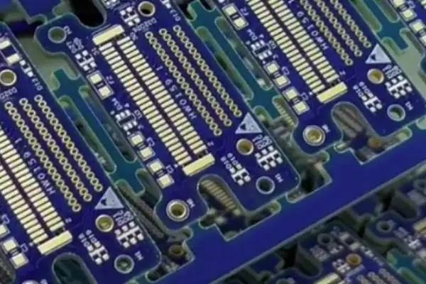
The etching process is often underestimated – the smoothness of the trace edges directly affects the accuracy of impedance control.
Once, we compared the etching results of two different manufacturers and found that one of them produced microstrip lines with jagged, uneven edges, leading to completely uncontrolled standing wave ratios.
The lamination process is an even greater test of technical expertise.
A misalignment of just a few micrometers in a multilayer board can compromise the entire circuit’s performance, so temperature and humidity control in the workshop must be strictly maintained to an almost obsessive degree.
I’ve seen some manufacturers skip the expansion and contraction compensation step to save costs, only to have to scrap entire batches of boards during mass production, resulting in even greater losses.
Now, more and more projects are requiring laser direct imaging technology, which does solve the alignment error problems of traditional exposure methods, but the equipment investment is not insignificant. It all comes down to how manufacturers weigh short-term costs against long-term competitiveness.
Speaking of surface treatment, we recently discovered that chemical immersion silver offers more significant advantages in high-frequency applications than expected. Although oxidation is a troublesome problem, for certain specific applications, this risk is worth taking.
The testing phase is the easiest to be fooled in – using a regular network analyzer to measure microwave frequencies simply doesn’t reveal the true performance. The vector network analyzer in our lab costs enough in annual calibration fees to buy a new device, but this investment is essential, because data credibility is paramount.
The longer I work in this field, the more I realize that microwave circuit board manufacturing is like working with precision instruments; every detail must be meticulously considered. Sometimes customers think we’re being overly critical, but anyone who has actually used precision boards understands that a small difference can lead to a huge discrepancy.
I’ve always felt that choosing a microwave circuit board is a bit like choosing a partner – a flashy appearance doesn’t necessarily mean a good match. Manufacturers who constantly boast about low-loss materials often fail to mention one fact: in practical applications, the stability of the board material is more important than the theoretical parameters.
I remember one time our team chose a high-end PTFE material to achieve an extremely low dielectric constant (Dk), and we ended up making a big mistake. This material was too sensitive to temperature; its performance fluctuated significantly during summer testing. Later, we discovered the problem was a mismatch in the thermal expansion coefficient of the board material. This taught me that instead of obsessing over the tangent delta (Tanδ) value to three decimal places, it’s more important to first confirm the operating temperature range.
Many microwave PCB manufacturers like to exaggerate the capabilities of ceramic-filled materials, but those who actually do RF design know there’s no magic bullet. Last time, for a millimeter-wave project, we tested three different PTFE substrates with varying filler ratios, and the most ordinary hydrocarbon material performed the most stably. The key is to have the manufacturer provide test curves for the actual frequency band; relying solely on datasheets can lead to significant problems.
I’ve seen too many engineers waste time on simulation and optimization while neglecting fundamental issues. For example, the phase consistency of boards from different manufacturers using the same material can vary tenfold, which is far more important than the material’s inherent loss. Once, we received a batch of boards where the microstrip lines had jagged edges, leading to poor VSWR. We traced it back to the manufacturer using dull cutting tools to save costs.
Now, for new projects, I always ask the manufacturer to send sample boards so I can build a test setup and run temperature drift experiments myself. Some manufacturers claim a Tanδ as low as 0.001, but the actual frequency-dependent curve isn’t flat at all. Recently, we found that a certain domestic modified PPO material was more reliable than imported PTFE in the Ka-band, at only one-third the price.
A truly good board material should be like an old friend – not necessarily spectacular, but reliable. For a phased array antenna project, we abandoned materials with slightly better individual specifications and chose a type with better processing compatibility. As a result, the mass production yield increased by 40%. Microwave circuit boards are ultimately meant to be products, not works of art in a laboratory.
Sometimes, watching young colleagues obsess over material parameters makes me laugh. Twenty years ago, we used ordinary FR-4 for 2.4GHz routers, and they ran stably for ten years. Now, everyone wants nano-ceramic materials, but in many scenarios, it’s simply over-engineering. A good microwave circuit board manufacturer should help customers balance performance and cost, not just push expensive materials.
Recently, while trying to combine high-speed digital boards and microwave circuits on the same board, I discovered an interesting phenomenon: some materials with average high-frequency performance are actually more stable in mixed designs because of better thermal expansion matching. This reminds me of what my mentor said – microwave engineering is the art of compromise; textbooks won’t teach you these things.
When selecting components for a security monitoring system, most attention goes to
Behind the mobile signals we rely on daily lies the sophisticated engineering
Many assume that wireless communication PCBs require expensive high-frequency materials. This guide
- 중소규모 배치 생산 전문가
- 고정밀 PCB 제작 및 자동화된 조립
- OEM/ODM 전자 프로젝트를 위한 신뢰할 수 있는 파트너
영업 시간: (월~토) 9:00~18:30