
Incorporating circuit boards is not just assembly, but also considers systemic integration.
We often regard electronic products as a glossy whole, but ignore the
I recently had a conversation with a friend working in the smart wearables sector and noticed an interesting phenomenon: their team spent over six months searching for a semiconductor flex PCB manufacturing partner, encountering numerous pitfalls along the way. The most surprising discovery was that many manufacturers—despite claiming they could handle the work—were unable to guarantee even the most basic flex-cycle durability.
One particular supplier hyped up their samples to the skies; yet, when we received them and performed a simple flex test, micro-cracks immediately appeared. While such issues might be marginally acceptable in the consumer electronics realm, they would be absolutely catastrophic in medical or industrial application scenarios.
In reality, determining whether a manufacturer is reliable doesn’t require counting the number of certifications displayed in their showroom. The true litmus test is whether they dare to grant you full access to their entire production workflow—especially the final stages.
I recall one instance where we were auditing a factory; their engineers led us directly to the equipment zone in a corner of the workshop, pointed to a dynamic flex test currently in progress, and said, “Feel free to adjust the parameters at any time to verify the results yourself.” That level of transparency was far more reassuring than any marketing brochure could ever be.
Many manufacturers today tend to focus heavily on material thermal resistance. While that is certainly important, the more common failure mode in real-world applications is circuit breakage caused by repeated flexing. A truly competent manufacturer should be able to customize a solution based on your specific application scenario—after all, the flex-cycle durability requirements for a smartwatch band are on a completely different magnitude than those for an industrial sensor.
I particularly appreciate suppliers who proactively inquire about the specific usage context of your product. They might even offer recommendations during the design phase regarding specific areas that require reinforced protection. This kind of insight is typically derived from the accumulation of real-world case studies—knowledge that extends far beyond the scope of standard, generic manufacturing protocols. I recall an instance where we encountered a thorny problem: we needed to achieve high-frequency signal transmission on an extremely narrow flexible circuit. At the time, our partner’s engineers immediately pulled out their internal data to demonstrate how different routing layouts impacted signal integrity. This kind of practical, real-world experience proved far more valuable than mere theoretical parameters.
Ultimately, selecting a semiconductor flexible PCB manufacturer is akin to choosing a surgical partner; simply possessing a fine scalpel isn’t enough—what truly matters is the surgeon’s experience and their judgment in the heat of the moment.
Having spent a good number of years navigating the ins and outs of this industry, I’ve observed a rather interesting phenomenon. When the topic of high-precision semiconductor flexible PCB manufacturing arises, many people’s first instinct is to focus on the sophistication of the equipment or the complexity of the processes involved. While that is certainly true, I’ve always felt that the factors truly determining the final quality are often the subtle details—the ones that are easily overlooked.
Take, for instance, the vexing issue of material expansion and contraction. You might invest a fortune in top-tier equipment, and your engineers might calibrate the parameters with absolute precision; yet, once the material passes through the lamination press, its dimensions may shift ever so slightly. This minuscule deviation—this tiny discrepancy—is enough to render all your previous efforts completely futile. This isn’t merely a matter of equipment precision; it is a test of the depth of your understanding regarding the inherent characteristics of the materials you are using.
I recall a specific project where we ran into trouble while attempting to control line widths on a multilayer board. Theoretically, the line widths depicted in the design schematics were flawless. However, on the actual production line, the minute expansion and contraction of each individual material layer compounded upon one another, resulting in final alignment deviations that were virtually imperceptible to the naked eye.
In such situations, those so-called “standard procedures” prove largely ineffective. We were compelled to work side-by-side with our supplier, conducting repeated tests to document the actual behavior of the materials across different batches and varying environmental conditions, gradually—and painstakingly—developing our own proprietary set of compensation techniques. It was an incredibly grueling process.
Speaking of line widths, the industry is currently in a race to achieve ever-finer circuitry. However, I’ve noticed a common misconception: many people assume that simply making the lines thinner is the sole objective.
In reality, stability and consistency are far more critical. What good is it if you manage to achieve a 20-micron line width in one batch, only to see it fluctuate to 30 microns in the next?
It would be far more valuable—and practical—to maintain a stable, consistent line width of 25 microns right from the very start.
When selecting a semiconductor flexible PCB manufacturer to partner with, I place particular emphasis on their mindset and capabilities regarding the resolution of such issues. A truly exceptional manufacturer is not merely a passive executor of instructions.
They are a partner capable of sitting down with you to analyze and pinpoint the root causes of the problems at hand. Sometimes, the root of the problem lies in the front-end design phase.
For instance, if the circuit density in a specific area is excessively high, the subsequent lamination process can easily result in localized deformation due to uneven stress distribution, thereby compromising the final line width precision. Ultimately, this is a systems engineering challenge; every node is intricately interconnected. Merely striving for perfection in a single isolated step holds little significance. The true challenge lies in orchestrating the entire system to work in perfect harmony, while minimizing—or ideally eliminating—uncontrollable variables.
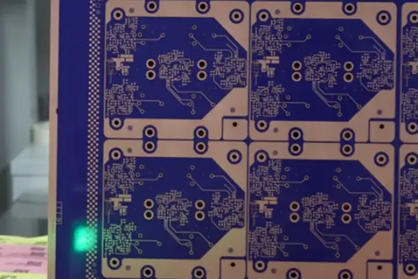
I have always held a deep admiration for manufacturers capable of successfully producing flexible printed circuit boards (PCBs) for semiconductor applications. It wasn’t until I toured the production line of a semiconductor flex PCB manufacturer a few days ago that I truly grasped the magnitude of their expertise. Inside their workshop, the digital readouts on the temperature and humidity monitors were constantly fluctuating—right down to the second decimal place. In such an environment, one feels compelled to regulate even the rhythm of one’s own breathing. The sight of the workers clad in protective suits reminded me of a hospital operating room; yet, instead of wielding scalpels, they were manipulating PCB substrates as thin as sheets of paper. This level of precision transcends the scope of conventional electronics manufacturing.
An engineer there confided in me that their most vexing challenge isn’t circuit design itself, but rather the material’s coefficient of thermal expansion and contraction. While a standard PCB might be rendered useless after being bent just a few times, semiconductor applications demand substrates capable of withstanding tens of thousands of repetitive flex cycles. I recall him holding a semi-finished board up to the light, gesturing as he asked, “Don’t these copper traces look just like a network of blood vessels?” In reality, they are far finer than blood vessels, with the narrowest traces measuring only a few microns in width. At such a microscopic scale, even a speck of dust floating in the air can become a formidable obstacle.
Many people assume that the semiconductor industry is primarily a contest of chip design prowess; however, I believe the true bottleneck lies in the back-end interconnects. Last year, a specific project encountered a critical failure: excessive tolerances in the PCB used during the packaging stage caused frequency drift across an entire batch of chips. The issue was finally resolved only after switching to a supplier capable of performing micron-level compensation. This incident served as a stark reminder that even the most brilliant chip design requires a reliable physical substrate to function effectively.
There is a fascinating trend emerging within the industry right now: some PCB manufacturers are establishing their own dedicated testing laboratories to conduct in-depth research on material fatigue data. They even go so far as to dispatch samples to various climatic zones for testing—ranging from the scorching heat of the desert to the bitter cold of the polar regions. This seemingly “low-tech” approach has, paradoxically, enabled them to accumulate a unique body of proprietary expertise. I once observed them using a high-speed camera to film the bending process of a PCB; when played back in slow motion, the copper foil appeared to ripple and undulate like ocean waves. It was then that I realized the true essence of “flexibility” in this context is not merely softness, but rather a state of elastic precision. Several recent cases have left me particularly astonished, revealing that some manufacturers have already begun utilizing semiconductor fabrication processes to produce circuit boards—for instance, by employing sputtering techniques to deposit copper onto polyimide substrates. While this method entails higher costs, it allows for sub-micron-level precision, making it uniquely suited for high-frequency signal transmission. One of our clients, a radar sensor manufacturer, reported that after switching to this process, their signal loss dropped by a staggering 40%.
In truth, when selecting a supplier, what I value most is not technical specifications, but rather their almost obsessive attention to detail. I once observed a quality inspector examining circuit traces under a microscope; he would scrutinize the same sample three separate times—first to inspect the traces themselves, second to examine the dielectric layer, and third to check for burrs or irregularities along the edges. This level of scrutiny went beyond even the client’s own mandated standards, yet the manufacturer voluntarily implemented this rigorous, three-tiered inspection protocol.
Ultimately, success in this industry boils down to one’s mastery of the microscopic realm. The enterprises truly worthy of trust are those that have internalized micron-level precision until it becomes second nature—a reflex embedded in their very operational DNA. After all, when circuit traces are finer than a human hair, reliability trumps mere cleverness every time.
When selecting a supplier for semiconductor flexible PCBs, I adhere to a specific routine: I first observe how they handle the “invisible risks.” Much like a black hole in the cosmos, the greatest dangers are rarely the obvious ones—such as the quoted price—but rather the quality pitfalls lurking deep within the manufacturing process itself.
I recall visiting the production line of a semiconductor flexible PCB manufacturer that proactively demonstrated their real-time monitoring system for their cleanroom facilities. This experience drove home a crucial realization: true professionalism lies not in merely remedying problems after they occur, but in seamlessly integrating preventive measures into every single detail of the operation. For instance, regarding ionic contamination testing, they retain and archive samples from every production batch for three years, ensuring complete traceability at any given moment.
Some suppliers are prone to boasting about the sophistication of their equipment, yet in practice, they fail to even maintain basic control over material stability. I have encountered instances where ordinary polyimide (PI) was passed off as a high-end material; initial tests appeared flawless, and the deception remained undetected until the client conducted high-temperature aging tests, at which point the substrate delaminated and the underlying issue was finally exposed. Such “hidden costs” are far more insidious than any figure listed on a price quote—for what they ultimately consume is the client’s trust.
Technical parameters such as “inter-layer alignment precision” may sound dry and academic, yet they serve as a critical differentiator between truly professional manufacturers and the rest. A competent supplier will proactively provide detailed data on material expansion and contraction for every batch—going so far as to invite the client to participate in the process calibration and fine-tuning. In contrast, manufacturers lacking such expertise will offer only vague assurances that their products “meet standards,” only to see their production yields fluctuate wildly—like a roller coaster ride—once mass production actually begins.
Nowadays, my partners and I place our primary emphasis on a supplier’s capacity for continuous improvement. For instance, one supplier established a joint laboratory dedicated specifically to researching the stability of high-frequency signal transmission. They even go so far as to frame and display the samples that failed during testing on their walls. This attitude toward problem-solving is far more reassuring than any formal certification.
Ultimately, selecting a supplier is much like assembling a band: simply judging the quality of the instruments is useless; what truly matters is the stability of the live performance. The partners who are proactive in exposing issues and willing to collaborate on process optimization are the ones truly worthy of long-term cooperation. After all, in the realm of precision manufacturing, the losses incurred from a single quality failure far outweigh the meager savings achieved during the procurement phase.
I recently had a conversation with a friend working in chip packaging and stumbled upon an interesting phenomenon: last year, their factory suffered a major setback—all because of a tiny flexible circuit board. They had initially believed that sourcing from a low-cost manufacturer of flexible PCBs for semiconductors would save them money; instead, they ended up losing millions. This incident reminded me of a problem often overlooked within the industry: we are all too prone to focusing our attention solely on the chips themselves, forgetting that the flexible materials connecting those chips are, in fact, the critical factor determining overall system stability.
The specific failure point in that case was quite typical: the supplier used standard additives during the electroplating process, resulting in a highly brittle plating layer. To make matters worse, that particular batch of boards had not undergone adequate thermal shock validation. Can you imagine? Those circuit boards—which appeared capable of bending with perfect ease—actually harbored extremely uneven internal stress distributions when subjected to temperature fluctuations. It was only after switching to a different vendor that they realized a truly reliable manufacturer would tailor their material formulations to suit specific application scenarios—for instance, by optimizing the Coefficient of Thermal Expansion (CTE) to precisely match the thermal expansion characteristics of the chips.
In truth, one can gauge the professionalism of a flexible PCB manufacturer for semiconductors simply by examining the design of their testing protocols. Some manufacturers naively equate testing with nothing more than basic electrical continuity checks; however, truly valuable testing should encompass mechanical fatigue trials, high- and low-temperature cycling, and microscopic structural analysis. I have witnessed technical teams that deliberately subject samples to tens of thousands of flex cycles, subsequently using microscopes to analyze the propagation patterns of cracks within the metal layers. Data derived from such rigorous analysis is infinitely more meaningful than a mere comparison of price quotes.
Nowadays, an increasing number of designs are adopting three-dimensional stacking architectures, which impose even more stringent demands on flexible circuit boards. For instance, in certain routing zones that must traverse the narrow gaps between stacked packages, the board thickness must be strictly controlled to within 0.1 millimeters—all while simultaneously ensuring the uncompromised quality of high-frequency signal transmission. This is precisely where traditional polyimide substrates tend to run into trouble. While newer materials—such as Liquid Crystal Polymer (LCP)—come with a higher price tag, their low moisture absorption and stable dielectric constants genuinely help mitigate a host of latent risks.
There is a subtle detail that many may overlook: failure in flexible PCBs during dynamic applications rarely manifests as a sudden, catastrophic fracture; rather, it typically results from the gradual accumulation of damage. It is much like repeatedly folding a sheet of paper; the crease will first turn white and become pliable before eventually tearing. Consequently, leading-edge manufacturers have begun developing predictive lifespan models. By monitoring trends in the Coefficient of Thermal Expansion (CTE), they can anticipate a product’s durability—a far more intelligent approach than attempting damage control after the fact.
During a recent visit to a research laboratory, I observed engineers utilizing simulation software to model material deformation under extreme temperature conditions. Once the thermal expansion coefficients for the chip, solder balls, and flexible substrate were fed into the system, it became vividly clear exactly where stress concentrations were occurring. While this “digital twin” technology entails a significant upfront investment, the cost pales in comparison to the financial and reputational fallout of a product recall following mass production.
Ultimately, selecting a flexible PCB supplier requires looking beyond the price tag; one must evaluate their accumulated technical expertise with the same scrutiny applied to choosing a strategic business partner. After all, when this thin, flexible circuit board serves as the “vascular system” connecting hundreds of billions of transistors, its reliability directly determines the overall robustness and longevity of the entire system.
Having spent a considerable amount of time in the semiconductor industry, I have gradually come to observe a rather intriguing phenomenon. Many people assume that identifying a reliable manufacturer of flexible semiconductor PCBs simply boils down to scrutinizing technical specifications; in reality, the scope is far broader than that. I have witnessed countless instances where an entire project required extensive rework—particularly those involving boards used in precision testing environments—solely due to an oversight regarding minute details.
I recall one specific instance where a partner supplied a batch of flexible PCBs that appeared flawless to the naked eye and met all specified technical parameters. However, shortly after being installed for machine testing, they began exhibiting signal drift. It took a painstaking troubleshooting process to discover that the culprit was residual ionic contamination on the board’s surface. Although invisible to the human eye, these charged particles—acting like countless tiny conductors in a humid environment—were disrupting the integrity of the test signals. The manufacturer subsequently had to invest significant effort into overhauling their cleaning protocols, bringing their control over ionic contamination to an almost obsessively rigorous standard before the issue was finally resolved.
This experience drove home the realization that “cleanliness” entails far more than simply donning a cleanroom suit. From the airflow dynamics within the manufacturing facility to the precise placement of every tool—and even the specific movements performed by the operators—virtually every detail has the potential to impact the final product. A long-term manufacturing partner of ours once told me that they go so far as to measure the static electricity levels of their packaging materials on a daily basis—all out of fear that even the finest dust particles might adhere to the circuit boards.
High-frequency testing is where a manufacturer’s true expertise is put to the test. Some boards perform flawlessly at room temperature, yet their performance begins to fluctuate the moment they are subjected to alternating cycles of extreme heat and cold. It is akin to putting electronic products through “endurance training”; one must simulate the most rigorous operating environments to uncover any potential weaknesses. I place particular value on a manufacturer’s willingness to invest the time in conducting such destructive testing—companies bold enough to push their products to the absolute limit are often the ones most confident in the quality of their work.
Nowadays, whenever I evaluate a new supplier, I make a point of scrutinizing the minute details of their daily operations. I look at seemingly trivial aspects—such as the frequency with which workers change their gloves, or the airtightness of the material transfer windows. A truly professional team seamlessly integrates a mindset of contamination prevention into every single step of their workflow.
Ultimately, a high-quality flexible printed circuit board (Flex PCB) must not only meet performance specifications but also stand the test of time. After all, semiconductor devices are often expected to remain in service for well over a decade; consequently, even the slightest defect could snowball into a major problem down the road.
During a recent conversation with a friend in the semiconductor industry, I observed an interesting phenomenon: many people assume that selecting a semiconductor Flex PCB manufacturer simply boils down to finding the facility with the newest equipment and the lowest price quote. In reality, however, the factors that truly determine the success of a partnership are often those invisible details—specifically, a manufacturer’s ability to meticulously handle the finer points of the production process.
Take the electroplating stage, for instance. During a tour of a factory’s production line, I noticed a specific detail: the operators, while calibrating the chemical bath concentrations, would adjust the immersion time based on the day’s ambient humidity. This seemingly casual, experience-driven adjustment actually has a direct and significant impact on the adhesion stability of the circuit traces.
The greatest concern with flexible materials is the risk of delamination following repeated bending. I have observed instances where manufacturers, in an effort to cut costs, simplify the via-filling process—a practice that leads to premature aging at the connection points.
I recall a sensor manufacturer once complaining that the flexible PCBs they procured suffered from severe signal attenuation in low-temperature environments. It was later discovered that the issue stemmed from insufficient plating uniformity, which resulted in impedance instability.
Truly professional manufacturers build sufficient process margins into their production workflows rather than rigidly adhering to standard parameters—after all, real-world application scenarios are far more complex than laboratory settings.
Speaking of which, another case comes to mind: a medical device manufacturer required flexible PCBs capable of withstanding hundreds of sterilization cycles daily. At the time, only two suppliers were able to pass the rigorous testing; the key differentiator lay in how they anticipated and managed the material’s thermal expansion and contraction properties.
Sometimes, the most fundamental steps are the ones that truly put a manufacturer’s expertise to the test. Take the seemingly simple via-filling process, for instance: depending on the manufacturer, the resulting product lifespan can vary by a factor of three or more.
In fact, there is a very intuitive way to gauge a supplier’s competence: observe whether they are willing to engage in in-depth discussions regarding past failures. Exceptional manufacturers are often more eager to share their improvement processes than to simply showcase flawless samples.
It is the accumulation of these minute details that ultimately creates the true distinction between manufacturers—for in the realm of precision manufacturing, the margin for error is simply too narrow.
I have long felt that many people’s understanding of flexible PCBs remains limited to the context of foldable smartphone screens. It wasn’t until I worked on a semiconductor testing project last year that I fully realized the truth: while they may both be flexible PCBs, the requirements for consumer electronics are a completely different ballgame compared to those for the semiconductor industry.
I remember a client—a manufacturer of wafer probe cards—coming to us to vent their frustrations. The boards produced by their previous supplier were chronically unstable; issues ranged from alignment deviations to a lack of chemical resistance in the materials. When we took over the project, we discovered that the root cause lay not in the manufacturing processes themselves, but in the underlying mindset. A typical flexible PCB factory might prioritize bend cycles and slimness, whereas the semiconductor industry demands a level of precision on an entirely different plane.
Take environmental control, for instance. I once toured the production line of a truly specialized semiconductor flexible PCB manufacturer; upon entry, one had to don a full anti-static suit and pass through three distinct air shower stages. Their workshop featured real-time temperature and humidity monitoring screens, and even the direction of airflow was clearly marked with arrows—details that ordinary factories wouldn’t even think to consider.
The testing phase presents an even starker contrast. The most extreme example I’ve witnessed involved simulating drastic thermal shock: a board was instantly transferred from an environment of over minus 60 degrees Celsius into one of 150 degrees Celsius, subjected to this grueling cycle hundreds of times over. This wasn’t merely a test; it was practically component torture. Yet, as the client explained, semiconductor equipment typically boasts a lifespan of a decade or more; without this level of rigorous testing, the components simply wouldn’t make the cut.
There was another small detail that I found quite interesting. Ordinary FPC manufacturers love to boast about how incredibly fine a line width they can achieve; however, in the semiconductor sector, stability is actually prized far more highly. I recall a specific project where we could technically have achieved a 20-micron line width, yet the client insisted on using 30 microns. He argued that the additional margin for error was far more critical than chasing after extreme performance parameters—a pragmatic mindset that left a deep impression on me.
Looking back now, if manufacturers claiming to produce high-end flexible PCBs cannot even pass basic chemical resistance tests, they really have no business venturing into the semiconductor field. After all, what is required here isn’t a flashy display of technical prowess, but rather rock-solid reliability; every single stage of the process serves as a rigorous test of the manufacturer’s mastery over minute details.
I recently had a chat with a friend who works in chip design, and he brought up a rather intriguing phenomenon: many people assume that advancements in chip performance are driven solely by upgrades in fabrication process technology. But what is the reality? Quite often, the true bottleneck—the element that actually “chokes” progress—turns out to be those unassuming interconnect components, such as the ultra-thin, ultra-precise flexible circuit boards embedded within high-end chips.
I recall that just last year, our team was evaluating several suppliers for this type of product. We had a specific project requiring a circuit board capable of undergoing multiple flex cycles within an extremely confined space without compromising signal integrity. We reached out to several standard PCB manufacturers, but they all admitted they lacked the capability to fabricate such intricate structures. It wasn’t until we connected with a manufacturer specializing exclusively in semiconductor-grade flexible circuits that the root of the problem became clear: the equipment precision at standard factories simply falls short of the micron-level control requirements demanded by the semiconductor industry.
That experience drove home a critical point for me: not every manufacturer that markets itself as a provider of flexible circuits actually possesses the genuine technical expertise to back up those claims. Some manufacturers are bold enough to accept orders even before they have fully grasped the fundamental material properties involved. Take polyimide, for instance—a commonly used material. The specific formulations and processing techniques employed by different manufacturers can vary wildly. Some versions may exhibit slight deformation when exposed to high temperatures, leading to signal distortion; conversely, a professional manufacturer of semiconductor-grade flexible PCBs will utilize specialized curing processes to ensure that dimensional stability remains tightly controlled within an extremely narrow tolerance range. The most extreme example I have ever encountered involved a mobile phone manufacturer that, in pursuit of a slim and lightweight design, adopted a substandard flexible connector. This resulted in an entire batch of products suffering from intermittent screen flickering issues. A subsequent teardown revealed that microscopic cracks had formed in the conductive traces at the flex points. While such a problem might merely degrade the user experience in standard consumer electronics, in the fields of medical devices or industrial control systems, it could pose a fatal safety hazard.
Nowadays, the demand for flexibility across many industries is no longer limited to simple bendability. For instance, automotive electronics require flexible circuits capable of withstanding high temperatures and high humidity, while wearable devices demand ultra-thin, stretchable substrates. Meeting these requirements necessitates that manufacturers possess a deep foundation in materials science, rather than simply recycling the manufacturing processes used for traditional rigid PCBs.
When selecting a supplier, what I value most is their willingness to engage in frank and open discussions regarding technical details. On one occasion, while touring a company’s production line, they proactively demonstrated how they conduct micron-level circuit inspections within a cleanroom environment. This level of meticulous attention to detail is far more convincing than any marketing collateral; after all, in the realm of precision manufacturing, a lapse in oversight at any single stage can lead to the complete failure of the final product.
I have observed many engineers struggle when it comes to selecting suppliers for semiconductor flexible PCBs. Sometimes, people fall into a common trap: assuming that the more advanced a manufacturer’s equipment is, the greater their overall capabilities must be. In reality, the true determinants of a successful partnership are often those invisible details that go unnoticed at first glance.
I recall a project last year that required a micro-pitch circuit design. We reached out to a semiconductor flexible PCB manufacturer that boasted ownership of state-of-the-art exposure machines. The samples they presented were indeed stunning, featuring trace widths as fine as one-third the thickness of a human hair. However, during the actual prototyping phase, we encountered a curious phenomenon: the exact same design file produced micron-level dimensional deviations across different production batches. It was only after visiting their factory that we discovered the root cause: although they claimed to operate a Class 10,000 cleanroom, fluctuations in temperature and humidity were significantly compromising the dimensional stability of the substrate material.
This experience brings to mind a contrasting case involving an established manufacturer that held ISO 13485 certification; they inspired a far greater sense of confidence. Their engineers proactively advised us that, beyond the trace widths specified in our design schematics, we needed to incorporate a margin for dynamic compensation. This is because flexible substrates undergo a phenomenon known as “stress relaxation” during the chemical etching process—a critical consideration, particularly in the context of semiconductor test probes.
Consequently, I now place a particular emphasis on evaluating a manufacturer’s depth of understanding regarding fundamental manufacturing processes. For instance, do they fully grasp the differences in shrinkage rates among various polyimide film materials when subjected to high temperatures? Can they devise a layered lamination strategy tailored to the unique structural requirements of a specific probe card? Such details often serve as a far more accurate gauge of a supplier’s true capabilities than mere equipment specifications.
A supplier I recently collaborated with left a profound impression on me. They have even established a comprehensive materials database, enabling them to recommend the optimal coverlay thickness based on the specific operating environment of the client’s product. On one occasion, a bending zone in our design required parameters that pushed the boundaries of conventional standards; their technical director personally led his team in developing three distinct stress simulation models to address the challenge.
Ultimately, selecting a flexible PCB supplier is akin to choosing a business partner; simply vetting their certifications and credentials is far from sufficient. You must assess their willingness to invest the time required to truly understand the logic behind your product, and their ability to offer expert guidance during critical junctures. After all, even the highest-tier ISO certification pales in comparison to the focused dedication of an engineer meticulously examining your circuitry under a magnifying glass.
Having spent over a decade in this industry, I have observed that many people’s understanding of flexible PCBs remains rooted in traditional paradigms. There is a common misconception that a flexible circuit board is adequate as long as it bends; in reality, the requirements are far more complex—particularly when integrating flexible circuitry with semiconductor technologies.
Take, for instance, a recent project we undertook where a client needed to embed sensors into a medical device. Standard flexible PCBs simply could not meet the specifications. This was because the device’s operating environment involved significant temperature fluctuations, coupled with extremely stringent demands for signal stability. It was in this context that the true value of a semiconductor-grade flexible PCB became evident.
I recall an interesting phenomenon I’ve frequently encountered: many engineers, during the initial design phase, tend to default to standard, off-the-shelf solutions—only to discover critical flaws once they reach the testing stage. On one occasion, we assisted a client in a redesign process, replacing their generic flexible PCB with a custom-engineered version; this single change elevated the reliability of the entire system to an entirely new level. This outcome was not merely a matter of material selection; it represented a fundamental shift in design philosophy.
When it comes to selecting a manufacturer, I believe the most critical criterion is whether they possess genuine R&D capabilities. While the market is currently flooded with manufacturers capable of producing flexible PCBs…
…very few truly possess a deep understanding of the specific requirements inherent to semiconductor applications. Some manufacturers may boast state-of-the-art equipment, yet their engineering teams lack a sufficiently profound grasp of semiconductor characteristics. This disconnect inevitably leads to performance issues once the product is deployed in real-world applications.
I have witnessed countless instances where product failures stemmed directly from a manufacturer’s inadequate understanding of materials science. For example, in high-frequency operating environments, standard polyimide materials simply cannot withstand the demands; specialized, modified materials are absolutely essential.
This is not merely a matter of cost; it is, fundamentally, a matter of accumulated technical expertise. In fact, many innovations today stem from cross-disciplinary applications. Take wearable devices, for instance: they must be lightweight, thin, and flexible, yet simultaneously guarantee high-quality signal transmission. This places extremely high demands on manufacturers.
We recently collaborated with a semiconductor company to develop a new product. Their initial concept was quite simple: they merely wanted a flexible connector board. However, after engaging in in-depth discussions, we discovered that what they truly required was a solution capable of handling high-frequency signal transmission. Such a gap between initial perception and actual need is a common occurrence in many projects.
I believe that when selecting a manufacturer, one should not focus solely on price quotes and equipment lists. What matters more is whether they can genuinely understand your specific requirements. Some manufacturers, despite their modest scale, possess profound expertise in niche fields and are therefore better positioned to provide highly specialized solutions. After all, in this industry, experience often counts for more than equipment.
We often regard electronic products as a glossy whole, but ignore the
Many assume that choosing China for PCB assembly is solely about saving
As an electronics engineer, I often view the Bare PCB as the
- 小・中ロット生産のエキスパート
- 高精度PCB製造と自動アセンブリ
- OEM/ODM電子プロジェクトの信頼できるパートナー
営業時間:(月~土)9:00~18:30