

What Documents Are Required for PCB Production: A Field Guide From Real Industrial Weighing Controller PCB Projects
Many engineers focus too much on technical parameters early on and overlook
Energy Storage System PCB: What a Decade of Field Operation Actually Demands
A conversation with a friend managing a new energy project surfaced a recurring complaint: a board in their energy storage system was failing repeatedly. The board in question was a PCB designed for energy management — and the failures were not random. They were systematic, driven by design and material decisions that had not accounted for what the operating environment would impose over time.
Many people assume that an energy storage system PCB is just a more robust version of a standard circuit board. The core task — storing and releasing electrical energy — sounds straightforward. But the power levels, the operating durations, and the environmental conditions that storage systems face make this a significantly more demanding engineering problem than it appears.
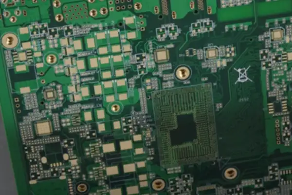
What the Operating Environment Actually Imposes
A large commercial or industrial energy storage station can experience instantaneous charge and discharge currents that are substantial. The copper conductors carrying those currents must do so with controlled resistive loss and heat generation. If the conductor path is undersized, thermally inadequate, or geometrically inefficient, the consequences range from accelerated aging of nearby materials to progressive thermal damage.
The BMS board that monitors and controls the battery pack adds a different dimension: it must measure cell voltages accurately in the same environment where large currents are switching. The magnetic fields produced by rapid current changes couple into any conductor loop in their vicinity. A BMS measurement path that forms a closed area — even a small one — in the plane of this magnetic field will have interference induced into it. If the interference magnitude approaches the signal magnitude, measurement errors follow. State-of-charge estimation errors accumulate, affecting charge efficiency and, potentially, safety margins.
Outdoor energy storage systems — utility-scale, commercial building, or grid support installations — operate across temperature ranges that can span one hundred degrees Celsius or more between seasonal extremes. The board must survive that temperature range not just at the material level but at the mechanical level: every thermal cycle stresses the solder joints that attach components to the board. After thousands of cycles, solder joint fatigue accumulates. Internal conductors that are imperfectly bonded to their dielectric develop micro-scale separations that progressively worsen. Failure occurs long after the last person inspected the hardware.
Material Selection for Long Service Life
Standard FR4 is adequate for many applications. For energy storage PCBs expected to operate for ten or more years in thermally variable environments, the glass transition temperature of the material is a relevant parameter. Below the glass transition temperature, the material behaves mechanically as a solid with relatively low thermal expansion. Above it, expansion accelerates significantly. If the glass transition temperature is too close to the operating environment’s maximum temperature, the board spends significant time in a mechanically softened state during peak load periods. Cumulative dimensional change — even very small — affects solder joint geometry over time.
High-Tg materials address this by raising the transition point above any temperature the system will realistically reach. The cost is higher material cost and sometimes more demanding processing requirements. For a system designed for a fifteen-year service life deployed in an outdoor industrial environment, the material cost difference is not the meaningful variable. The failure cost — replacement, system downtime, escalating maintenance — is.
A field observation during renovation of a storage facility that had been operating for over a decade was instructive. Some boards in the installation used premium materials and showed essentially no visible aging. Adjacent boards that had used cost-reduced alternatives showed visible discoloration and, in cross-section, early-stage delamination. The electrical performance of the degraded boards was still within specification at the time of inspection. But delamination that is progressing will eventually affect electrical performance, and it is a nonlinear process — the rate of degradation accelerates as the damage accumulates.
Surface finish selection for long-term reliability follows similar logic. ENIG provides consistently solderable surfaces that do not oxidize during storage. In high-humidity coastal environments, the finish choice affects corrosion resistance at connector and solder pad surfaces that will experience moisture exposure over the product’s life. These are not dramatic single-event failures — they are gradual degradation paths whose cumulative effect becomes visible years after installation.
BMS Signal Integrity: The Detail That Determines Accuracy
Analog measurement circuit layout is one of the most consequential and least discussed aspects of BMS PCB design. The accuracy of the voltage and current measurements that the BMS uses to estimate state of charge, state of health, and safety conditions depends entirely on the quality of the signal path from sensor to converter.
Star-topology grounding — routing each sensitive measurement circuit’s analog reference connection to a single common point, rather than sharing a ground conductor with other circuits — minimizes the error contributed by ground potential differences between measurement points. This is well established in precision analog design. Its implementation in BMS PCB layout is frequently compromised by density constraints or by designers who have not prioritized it.
The power supply network for analog measurement circuits should be isolated from the digital supply network. The switching noise present on a digital supply rail — generated by processor activity, memory access, and communication interface operation — can reach tens of millivolts in amplitude. If this noise appears in the analog measurement supply, it is indistinguishable from the signal being measured. A simple magnetic bead or small series resistor at the supply input to the analog circuit section, with adequate local bypass capacitance, provides effective isolation at low cost. Neglecting this isolation is a common source of measurement noise that is difficult to trace after the board is assembled.
High-Voltage Isolation at System Voltages
Systems operating at 1500V or higher introduce failure mechanisms that do not appear at lower voltages. Standard dielectric materials at normal spacing can exhibit partial discharge — localized ionization events within the dielectric or at air gaps that do not immediately cause complete breakdown but progressively erode the insulation. Partial discharge can occur at voltages well below the material’s nominal dielectric breakdown strength.
The mechanism is subtle. A small void in the dielectric, or an air gap between a conductor and the substrate surface, can experience local electric field intensification sufficient to cause ionization. The discharge energy is small; the current instruments used in production testing may not detect it. But each discharge event chemically degrades the surrounding material. The degraded region has reduced dielectric strength, which makes subsequent discharges more likely and more energetic. The process is self-amplifying until macroscopic failure occurs.
For energy storage systems operating at high voltage, the relevant specification is not just dielectric breakdown voltage but resistance to partial discharge over the expected service life. This requires selecting materials with high Comparative Tracking Index (CTI) ratings and specified partial discharge inception voltages, maintaining adequate creepage and clearance distances in the PCB layout, and performing partial discharge testing as part of qualification rather than inferring performance from static high-voltage tests. A board that passes a short-duration high-voltage hipot test may still be susceptible to partial discharge degradation under sustained operating voltage over years.
One failure analysis report on a converter board from an energy storage installation showed exactly this mode. The board had passed all production electrical tests. Cross-section analysis after field failure revealed a region of carbonized dielectric adjacent to a high-voltage conductor. The creepage distance at that location was within the standard specification for the rated voltage — but the design standard had been written for indoor, controlled-environment installations. The actual installation’s higher humidity created conditions where effective creepage distance was reduced. The margin that existed in the specification did not exist in the field.
Matching the Manufacturing Partner to the Application
Suppliers who produce commodity PCBs competently are not necessarily equipped to produce energy storage system PCBs reliably. The questions that distinguish capable suppliers for this application are specific to it.
Can the supplier demonstrate their process capability for high-voltage isolation design? Do they have experience with the creepage and clearance requirements applicable to the voltage class of the system? What is their approach to incoming material inspection for high-Tg laminates — do they test and document actual Tg values per lot, or do they accept the nominal specification from the material data sheet?
Thermal management capability — thermal via design, copper plane distribution, interface to external cooling — requires process understanding that goes beyond standard PCB production. A supplier who has produced boards for high-power applications where junction temperature management was a design driver has accumulated knowledge that a supplier working primarily on signal-level boards has not.
The conversation about a specific project should address the operating environment explicitly: geographic location, expected temperature range, humidity conditions, vibration profile if relevant. Suppliers who engage with this information to recommend material selections and processing specifications are providing engineering value. Suppliers who respond with a standard offerings list regardless of application context are not.
Long-Term Partnership and Supply Chain Stability
Energy storage projects have capital deployment timelines measured in years and asset lifetimes measured in decades. The PCB supplier relationship spans this period. A supplier who provides responsive engineering support during design validation, maintains process stability across production runs over multiple years, and manages material supply chains proactively during periods of shortage contributes to project success in ways that unit price comparison does not capture.
The supply disruptions that periodically affect specialty laminate materials — high-Tg FR4, low-loss materials for specific impedance targets — affect all buyers, but their impact on projects is modulated by how well the supplier has managed their material inventory and supply relationships. A supplier with strong upstream relationships and proactive inventory management can maintain delivery commitments during shortage periods that cause disruption for others.
The boards in an energy storage installation will carry current, manage battery safety, and enable system monitoring for the duration of the project’s service life. They will not be accessible for routine inspection. Problems that develop slowly over years become visible only when they have progressed far enough to affect system performance. The investment in getting the design right, the material selection right, and the manufacturing partner right pays back over the entire service period — not just in the first year after installation.
Many engineers focus too much on technical parameters early on and overlook
As someone who has worked in PCB outsourcing for years, I’ve found
Cramming a camera, amplifier, dual-mic array, and Wi-Fi radio into a palm-sized
- 小・中ロット生産のエキスパート
- 高精度PCB製造と自動アセンブリ
- OEM/ODM電子プロジェクトの信頼できるパートナー
営業時間:(月~土)9:00~18:30
Get quote, solution or any question, Andre always here to help