

What Documents Are Required for PCB Production: A Field Guide From Real Industrial Weighing Controller PCB Projects
Many engineers focus too much on technical parameters early on and overlook
Electric Vehicle Control PCB: Managing High Current, High Voltage, and Long-Term Reliability in One Board
Taking apart an old electric bicycle controller and finding a board with burned traces and bulged capacitors is a useful reminder of what happens when power electronics outpace their substrates. The difference between that failure and the control boards in current electric vehicles is not just scale — it is the entire engineering framework brought to bear on the problem.
Modern EV powertrains operate at current levels that reach hundreds of amperes during acceleration and regenerative braking, on voltage platforms that are increasingly standardized at 800 volts or above. Ordinary PCB copper traces cannot carry these loads without unacceptable resistive heating and voltage drop. The design of boards for these applications is a discipline that combines electrical engineering, materials science, thermal physics, and mechanical reliability into a single integrated problem.
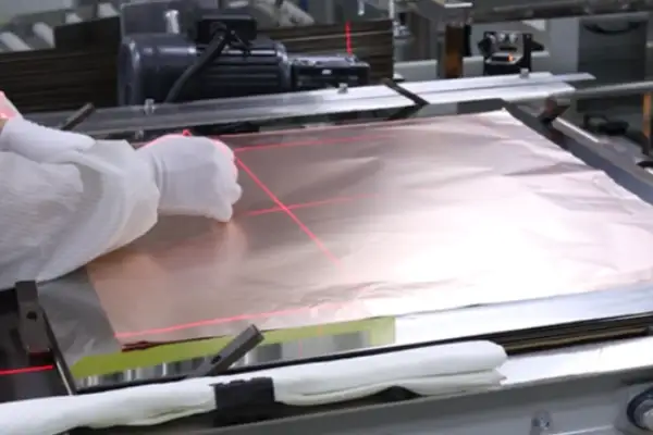
The Transformation of PCB’s Role in EVs
In the era of combustion engines, the PCB was a connecting substrate — a way to wire components together inexpensively. That role ended when electric drivetrains made the PCB central to the vehicle’s energy conversion chain.
The battery management system board monitors cell voltages at millivolt resolution, estimates state of charge, and controls charge and discharge profiles across the entire cycle of vehicle operation. The motor controller board converts DC bus voltage to three-phase AC with precise timing and amplitude control. The onboard charger converts grid AC to the DC voltage level of the battery pack. Each of these functions demands a board that is not simply adequate but performs reliably under the sustained electrical and mechanical stress of vehicle deployment.
This shift explains why the value attributed to high-quality EV control PCBs has increased as a fraction of system cost. A BMS board failure does not just disable one feature; it can render the vehicle unable to operate or, in more serious cases, allow battery conditions that create safety risk. The board’s quality is tied directly to the vehicle’s safety profile.
Copper Thickness Is Not the Complete Answer
The most common oversimplification in high-current PCB design is treating copper thickness as the primary variable to increase. Adding copper does reduce resistive loss and the heat generated in power paths. But beyond a certain thickness, the incremental benefit of additional copper is offset by the additional challenges it creates.
Very thick copper in a PCB stackup increases the thermal expansion coefficient differential between the copper and the dielectric material. During the thermal cycles that characterize EV operation — warm startup, full-power operation, cooling during parking — this differential generates mechanical stress at the copper-dielectric interface. After sufficient cycles, microscopic delamination or cracking can develop. The board that performed correctly when new degrades in ways that are not visible in standard electrical testing.
A more effective approach to high-current path design focuses on layout geometry before copper thickness. The current path should be as short and direct as possible. Right-angle bends and routing detours introduce local current density peaks that create localized heating. Spreading the current across multiple parallel conductors — rather than concentrating it in a single thick trace — achieves lower effective resistance and better thermal distribution simultaneously.
One concrete case: a design using 4-oz copper with a layout that allowed excessive trace length and several direction changes showed thermal hotspots at specific locations during high-load testing. A redesign that reorganized current flow paths and distributed the load differently, while using 2-oz copper, produced better thermal uniformity and lower peak temperatures. The additional copper weight was not the limiting factor; the current path geometry was.
BMS Signal Integrity in a High-Noise Environment
The BMS board faces one of the most demanding mixed-signal design problems in automotive electronics. It must measure battery cell voltages at millivolt resolution in an environment where high-current switching events in adjacent circuits generate electromagnetic disturbance that can easily reach tens of millivolts. The measurement must be accurate; the control decisions based on it affect battery longevity and safety.
Routing sensitive analog measurement paths in close proximity to high-current switching loops is the most common BMS design error. The di/dt in a fast-switching power loop generates a magnetic field that induces voltage in any loop formed by adjacent signal conductors. If the measurement path forms a closed loop — even a small one — with area in the plane of that magnetic field, the induced voltage adds to the measured signal as noise.
The design countermeasures are established: maintain complete physical separation between analog measurement circuits and power switching sections; use differential signal paths for all cell voltage measurements to reject common-mode interference; provide each functional supply domain with its own bypass network referenced to a single ground point; avoid routing measurement signal lines across power plane splits, which disrupts the return current path and creates the ground loops that admit noise.
For 800V system architectures, high-voltage isolation requirements become another design constraint. The creepage distance between conductors at different voltage potentials must meet IEC 60664 clearance and creepage requirements for the pollution degree and overvoltage category applicable to the installation. This is not a conservative adjustment to standard design rules — it is a different calculation entirely, and the required distances are substantially larger than what is appropriate for low-voltage circuits. Placing high-voltage isolation requirements into the board design without understanding this calculation produces boards that meet normal electrical tests but fail under high-voltage stress in field conditions.
Thermal Path Design From First Principles
Power semiconductors generate heat at their junctions. The thermal path from the junction through the component package, through the solder joint and PCB, to the cooling interface determines the junction temperature that the device operates at under load. Junction temperature directly affects device reliability and longevity: every 10 degrees Celsius increase in steady-state junction temperature roughly halves the expected lifetime of semiconductor junctions.
Thermal via arrays placed immediately beneath power component pads create low-resistance heat conduction paths through the PCB to its back surface. The effectiveness of these arrays depends on via diameter, spacing, and plating thickness. Underfilled vias or vias with thin plating walls conduct heat inefficiently. Good thermal via design requires specifying not just the via pattern geometry but the plating requirements needed for the thermal resistance calculation to be valid.
Metal base substrates — aluminum or copper — are used in some high-power applications because their thermal conductivity is orders of magnitude higher than FR4. The tradeoff is that electrical isolation must be maintained between the metal base and any electrically active conductors, which requires a thin dielectric layer whose thermal resistance limits the overall thermal path conductance. Embedded copper blocks or coin inserts in standard multilayer substrates offer an intermediate solution: local regions of high thermal conductance at the specific locations where power devices are mounted.
The mechanical dimension of thermal design is easy to overlook. The EV powertrain environment includes vibration from road surface, drivetrain operation, and wind. Components with significant mass — large capacitors, inductors, connector assemblies — apply mechanical force to their solder joints during vibration. If the board’s resonant frequency coincides with a vibration frequency present in the vehicle, amplitude is amplified and fatigue accumulation accelerates. Component placement and mechanical fastening must account for the vibration environment, not just the electrical requirements.
Manufacturing Standards and Their Meaning
IATF 16949 certification is often cited as a quality indicator for automotive PCB suppliers. The certification is meaningful — it establishes that a supplier’s production management system meets requirements that the automotive industry has determined are necessary for consistent quality. But it describes process management, not technical capability.
The engineering questions that reveal genuine automotive PCB competence go beyond certification: What experience does this supplier have with thick copper etching, and what line width tolerance control can they demonstrate? How do they handle high-voltage isolation design reviews? What lamination process adjustments do they make for asymmetric stackups with mixed copper weights? What failure modes have they encountered in automotive programs, and what process changes resulted?
Suppliers who can answer these questions with specific examples — not general assurances — have built the experience base that automotive programs require. A supplier’s willingness to describe a problem they encountered and how they resolved it tells more about their engineering capability than a capabilities list.
The Long-Term Reliability Perspective
Electric vehicles are consumer products with manufacturer warranty periods and expected service lives measured in years, deployed in environmental conditions ranging from arctic winters to desert summers. A PCB that meets all specifications at the end of production must still meet them after a decade of operation.
This demands thinking about material aging, solder joint fatigue accumulation, connector contact degradation, and coating integrity in ways that are not captured by standard product testing. The relevant engineering knowledge is accumulated through field return analysis on prior programs, through accelerated life testing that models specific failure mechanisms, and through collaboration with suppliers who have enough automotive program experience to have encountered these failure modes.
The board is not visible from outside the vehicle. Its quality does not appear in marketing materials. But it determines whether the energy stored in the battery pack reaches the motor efficiently and safely, whether the regenerative braking captures energy reliably, and whether the system operates correctly across the full service life the vehicle is designed for. That invisible function is the foundation on which everything else depends.
Many engineers focus too much on technical parameters early on and overlook
As someone who has worked in PCB outsourcing for years, I’ve found
Cramming a camera, amplifier, dual-mic array, and Wi-Fi radio into a palm-sized
- 小・中ロット生産のエキスパート
- 高精度PCB製造と自動アセンブリ
- OEM/ODM電子プロジェクトの信頼できるパートナー
営業時間:(月~土)9:00~18:30
Get quote, solution or any question, Andre always here to help