
How to Choose an Excellent Semiconductor Flex PCB Manufacturer?
While collaborating with a smart wearables team to select a semiconductor flex
Lately, I’ve been giving a lot of thought to the subject of circuit board thermal management. Sometimes, I observe engineers racking their brains—tweaking heat sink shapes or fan speeds—just to shave off a few degrees of temperature difference; yet, the most fundamental issue may actually lie within the circuit board’s own thermal conduction pathway.
I recall a situation I encountered last year while debugging a motor driver board. After the device had been running for just half an hour, the MOSFET temperatures skyrocketed to critical levels. I tried swapping in three different heat sinks, but none yielded any significant improvement. It wasn’t until I sent the aluminum-based PCB to a laboratory for thermal imaging analysis that I discovered the root of the problem lay in the insulating layer material. Although its nominal thermal conductivity met the required specifications, actual testing revealed that heat was getting “stuck” between the components and the metal substrate, unable to flow outward.
This design concept—circuit boards featuring a metal baseplate—is truly fascinating. It essentially lays down a “highway” for heat-generating components, allowing heat to be rapidly conducted from the chips to the metal base, and subsequently dissipated into the environment via the heat sink. However, whether this thermal pathway remains unobstructed depends critically on the performance of the insulating layer—the key gatekeeper in this process.
During a visit to a PCB製造 facility, I witnessed a comparative experiment: two aluminum-based PCBs of identical specifications were tested side-by-side. The board utilizing a standard epoxy resin insulating layer exhibited chip temperatures that were more than ten degrees higher than the board utilizing a ceramic-filled insulating material. This reminded me of my childhood winters: although a traditional cotton-padded jacket might be thick and bulky, it offers less thermal insulation than a down jacket—precisely because the thermal conductivity of down feathers is much closer to that of air. The selection of the insulating layer follows the same logic: thicker isn’t necessarily better; rather, the goal is to strike a balance between thermal conductivity and dielectric strength.
Nowadays, many manufacturers are beginning to focus on the peel strength of insulated metal substrates. After all, if the bond between the copper foil and the insulating layer is weak, even the most sophisticated thermal design is rendered useless. I have encountered instances where inexpensive circuit boards developed blistering in their traces after a period of use—a phenomenon caused by a mismatch in the thermal expansion coefficients of the materials under high-temperature conditions.
In practical applications, there is another easily overlooked detail: the drilling process for metal substrates. While standard FR4 boards can be processed directly using CNC drilling machines, aluminum-based substrates require specialized carbide drill bits, necessitating specific adjustments to both spindle speed and feed rate. On one occasion, a prototype board suffered a short circuit during installation because drilling burrs had not been properly removed; consequently, the insulating layer was punctured by a mounting screw.
Speaking of thermal dissipation paths, I like to visualize the process as a relay race. Heat originates at the chip and is successively transferred through the solder, copper foil, insulating layer, and metal base layer; every single stage of this journey must perform flawlessly. Among these stages, the insulating layer often represents the segment of the track most prone to becoming a thermal bottleneck.
During recent testing of novel Gallium Nitride (GaN) devices, we observed an interesting phenomenon: when the switching frequency exceeded 100 kHz, traditional thermal grease would undergo curing shrinkage, creating microscopic voids that actually increased the interfacial thermal resistance. It was only after switching to phase-change thermal interface materials that the temperature profile finally stabilized. This demonstrates that as power density continues to rise, the thermal management of every single connection point requires a thorough re-evaluation.
In fact, observing the evolution of computer motherboards offers valuable insights. From early single-sided layouts to modern multi-layer boards featuring embedded copper blocks for heat dissipation, the fundamental objective remains the same: optimizing the thermal flow path. Perhaps the future holds even more intelligent thermal management solutions—such as embedding miniature heat pipes directly within the insulating layer, or utilizing “smart” materials with variable thermal conductivity.
Whenever I disassemble imported electronic equipment, I invariably notice that their circuit boards prioritize a holistic, systemic approach to thermal design. Rather than simply stacking up high-conductivity materials, they focus on configuring the thermal resistance at each stage in the most rational and balanced manner possible. This, perhaps, is precisely where we can learn from them: thermal management is not a solo act performed by a single component, but rather a collaborative effort involving the entire system working in concert. Gazing at the remnants of disassembled circuit boards scattered across my workbench, I was struck by a sudden realization: thermal design is much like controlling the heat in cooking—one must adjust the heat transfer method based on the specific characteristics of the “ingredients” at hand. Sometimes, a shift in perspective proves far more effective than blindly attempting to boost cooling capacity; for instance, by converting a concentrated heat source into a distributed layout, or by utilizing the metal substrate itself as an auxiliary heat-dissipation surface.
These experiences have taught me a fundamental lesson: effective thermal management is not about fighting against the laws of physics, but rather about learning to work with them. Much like flood control—which cannot rely solely on erecting barriers—heat must be allowed to flow naturally along a carefully engineered path.
While working on circuit designs, I’ve observed an interesting phenomenon: the moment thermal management is mentioned, many people immediately gravitate toward copper substrates. It is true, of course—and common knowledge—that copper possesses exceptional thermal conductivity; however, the reality of the situation is often far more complex than one might initially imagine.
A project from last year stands out vividly in my memory. Our team was designing a portable outdoor power supply unit, and in our initial pursuit of optimal thermal performance, we opted directly for a copper substrate. However, during the prototype testing phase, we encountered a significant issue: while the heat dissipation was indeed outstanding, the total weight of the device exceeded our projected target by nearly 40%—a catastrophic outcome for a product designed with portability in mind.
We subsequently re-evaluated our requirements and discovered that an aluminum substrate—paired with a specially treated insulating layer—would be entirely sufficient to meet our specifications. Here lies a subtle detail that many tend to overlook: the thermal conductivity of the insulating layer often proves to be a greater bottleneck than that of the metal substrate itself. We tested various grades of insulating materials and found that, provided the appropriate dielectric medium is selected, the overall thermal performance of an aluminum-based board can closely rival that of a copper-based board.
When it comes to cost, I believe one must look beyond the unit price of the raw materials. On a previous project, we selected a low-cost substrate in an effort to trim the budget; however, once we entered mass production, we struggled to achieve an acceptable yield rate, and the subsequent costs incurred from rework and repairs ultimately proved to be even higher. This is particularly true for specialized materials such as Insulated Metal Base PCBs; while the apparent price difference on paper might seem to be a mere 20% to 30%, the hidden costs stemming from increased processing complexity and higher scrap rates often end up far exceeding initial expectations.
Nowadays, whenever I am tasked with selecting materials for a new project, my first step is to clearly define the device’s actual operating environment. If the device requires frequent mobility, the lightweight advantage of an aluminum substrate becomes the obvious choice; conversely, if it is a stationary device with extreme thermal management requirements, then the additional investment in a copper substrate is well justified. The key lies in finding the optimal balance between performance and cost—rather than blindly chasing after the theoretically “best” technical specifications. I recently handled a particularly interesting case: the client initially insisted on using a high-specification copper-based substrate. We suggested, however, that they first try optimizing their circuit layout. As it turned out, simply by rearranging the placement of a few heat-generating components, we were able to meet all temperature requirements using a standard aluminum-based substrate. This experience reinforced my conviction that effective design must always take a holistic, system-level approach.
I remember being quite surprised the first time I encountered an insulated metal substrate in the lab—it was remarkable that such a thin layer of material could withstand such drastic temperature fluctuations. As I gained more experience with them, however, I realized that their underlying design is far more complex than it appears on the surface.
I recall a specific project involving the use of aluminum substrates for automotive equipment testing, which yielded some fascinating results. Initially, the engineers were primarily concerned about heat dissipation; however, after extensive troubleshooting, they discovered that the true bottleneck—the critical limiting factor—was actually the stability of the insulating layer.
While disassembling samples on one occasion, I noticed a subtle but significant detail: the insulating layers on substrates intended for industrial equipment were substantially thicker and more robust than those found in consumer electronics. This disparity, in fact, reflects the distinct reliability demands imposed by these different application environments.
Nowadays, when discussing these types of materials, many people tend to focus exclusively on thermal conductivity parameters. However, based on my observations, the factor that truly determines a product’s longevity is the performance of the insulating layer under conditions of thermal cycling—the repeated transition between hot and cold extremes. Consider, for instance, an electric vehicle parked outdoors during a northern winter; the circuit boards within that vehicle must endure temperature fluctuations far more severe than those typically simulated in a laboratory setting.
The most extreme case I have ever encountered involved a custom-built experimental apparatus commissioned by a research institution. The device was required to operate continuously within a vacuum environment; however, the insulating layer of the standard substrate initially selected developed microscopic cracks due to the extreme temperature differentials. The issue was ultimately resolved only after switching to a specially treated metal substrate. This experience served as a stark reminder that material selection cannot be based solely on standard technical specifications.
What I find most fascinating about these materials is their inherent adaptability. For example, even within the automotive sector, the requirements for LED headlights differ completely from those for high-power electric motors. The former prioritizes uniform heat dissipation, whereas the latter demands the ability to withstand the thermal stress generated by sudden, high-magnitude current surges.
I recently applied this same line of reasoning while helping a friend upgrade his home audio system. Although the power output was relatively modest, I opted for a copper-based substrate featuring a thick insulating layer to ensure optimal sound quality and stability. The results exceeded our expectations, reinforcing my belief that, on occasion, deliberately exceeding standard specifications can actually lead to a superior user experience. Ultimately, material design must always return to the context of real-world application scenarios. Take outdoor LED displays and medical equipment, for instance: although both utilize metal substrates, the former must account for rainwater erosion, while the latter demands absolute reliability over long-term operation. Such contextual differences are often far more critical than mere technical specifications.
Whenever I test these materials, I am reminded that “high performance”—so-called—is not about blindly maximizing a single metric, but rather about identifying the most balanced solution within a specific operating environment. After all, the variables encountered in the real world are far more numerous and complex than those found in a controlled laboratory setting.
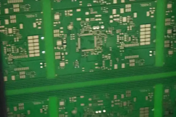
I’ve recently been pondering a rather interesting trend: an increasing number of electronic products are now incorporating circuit boards featuring a metal baseplate. In the past, we typically envisioned a circuit board as nothing more than a thin, green sheet; today, however, the landscape has shifted. This is particularly evident in high-power devices, where you will often discover that the PCBs are mounted atop a substantial, heavy-duty metal base.
I recall an instance last year when I was helping a friend repair a piece of stage lighting equipment; I opened it up to take a look inside. The circuit board was mounted directly onto an aluminum heat sink. At the time, I thought it was an incredibly clever design. Heat generated by the chips was transferred directly into the metal substrate, completely eliminating the need for additional heat fins. The underlying design philosophy behind these “Insulated Metal Base PCBs” is, in fact, quite intuitive.
However, metal substrates are not a universal panacea. I learned this the hard way once while designing a circuit for high-frequency signal processing. Although the thermal dissipation was excellent, the inherent characteristics of the metal substrate significantly compromised signal integrity. I ultimately had to switch to a specialized composite substrate to resolve the issue. Thus, the choice of substrate must always be dictated by the specific requirements of the application scenario.
Nowadays, whenever engineers think about thermal management, their first instinct is often to add fans or heat sinks. In reality, addressing the problem at its source can be far more effective. By mounting heat-generating components directly onto a metal substrate, the efficiency of heat conduction is vastly improved. I’ve even conducted comparative tests: under identical power loads, a circuit utilizing a metal substrate ran more than ten degrees cooler than one built on a standard FR-4 board.
The selection of the metal material itself is another fascinating aspect. Aluminum is inexpensive and lightweight, though its thermal conductivity is merely average. Copper offers superior thermal conductivity, but it comes with increased weight and higher costs. In certain specialized applications, stainless steel may be employed; while its thermal conductivity is somewhat lower, it boasts excellent corrosion resistance. Ultimately, the choice requires a careful balancing act based on the specific demands of the project.
Designing the insulating layer is also a technical art form in itself; if it is too thick, it will impede thermal conduction. If the insulating layer is too thin, there is a risk of insufficient electrical isolation. I’ve seen instances where manufacturers, in pursuit of maximum heat dissipation, made the insulating layer exceptionally thin. The result was system failure when the devices were exposed to humid environments. Striking the right balance here is absolutely critical.
Nowadays, an increasing number of industrial devices are utilizing PCBs equipped with metal baseplates—particularly high-power motor drivers and power supply units. After all, reliability takes precedence over everything else.
However, to be honest, I believe this design philosophy could stand to be more widely adopted. Many consumer electronics products are now drawing increasingly higher power loads.
If the concept of metal-substrate design had been embraced sooner, the service life of many products could likely have been extended significantly.
When I first started working with Insulated Metal Base PCBs, I was a bit confused; I assumed that heat dissipation relied solely on that metal baseplate. It wasn’t until later that I realized the truly fascinating element is actually that thin insulating layer sandwiched in the middle. This layer has to simultaneously contain the electrical current—preventing it from straying—while rapidly channeling heat away. It’s almost like asking a goalkeeper to double as a delivery courier.
I recall a specific instance during material testing where we discovered that even a slight tweak to the insulating layer’s chemical formulation could result in a massive difference in thermal conductivity. Sometimes, in the quest for superior thermal performance, one ends up sacrificing dielectric strength; navigating this inherent trade-off often proves to be a major headache in real-world projects.
In fact, many manufacturers are currently experimenting with novel composite materials—for instance, by embedding ceramic particles within a resin matrix. This approach preserves the material’s flexibility while simultaneously boosting heat dissipation efficiency, though it does, admittedly, drive up production costs significantly.
I find it particularly instructive to observe how the insulating layer performs under varying temperature conditions. Some materials perform admirably at room temperature but begin to falter once exposed to high-temperature environments; issues related to material aging—particularly after prolonged operation—can become quite pronounced.
When selecting a substrate, one cannot simply look at the thermal conductivity parameters in isolation; the specific application environment must also be taken into account. If the device is destined for an environment subject to significant vibration, for instance, one must prioritize the adhesion strength between the insulating layer and the metal base to prevent delamination from occurring during operation.
The most extreme case I’ve ever witnessed involved a manufacturer who, in an attempt to cut costs, made the insulating layer excessively thin. During the final assembly and testing phase, the layer suffered a complete dielectric breakdown, rendering the entire PCB board—and the device—useless. Such cautionary tales serve as a stark reminder that one simply cannot compromise on the critical parameters of layer thickness and voltage withstand capability.
A truly effective design ensures that heat flows smoothly through the insulating layer to reach the metal baseplate, all while providing robust protection for the electrical circuitry. Achieving this delicate balance requires the materials engineer to possess a deep and nuanced understanding of interfacial characteristics. Sometimes I feel that the most fascinating aspect of this industry lies in the handling of unseen details. A minor tweak in processing can potentially double the lifespan of an entire circuit board—though, of course, it could just as easily backfire. It all comes down to whether one’s accumulated experience is truly up to the task.
When working on LED projects, I initially found myself somewhat conflicted regarding the choice of insulated metal substrates. Many people would immediately recommend aluminum substrates; looking at the datasheets, the parameters certainly seemed impressive, and the price was right. However, I soon discovered that in real-world applications, aluminum isn’t always the optimal choice.
On one occasion, we designed an outdoor lighting product utilizing an aluminum substrate. After operating for a period in an environment with significant temperature fluctuations, microscopic cracks began to appear in the solder joints. Subsequent inspection revealed that this was a stress-related issue caused by a mismatch in the coefficients of thermal expansion. Although the numerical difference was merely a few parts per million (ppm), its impact during prolonged thermal cycling proved to be far from negligible.
Copper-based insulated metal substrates have left a particularly strong impression on me; their heat dissipation efficiency is truly exceptional, especially when handling high-power LEDs. However, cost remains a very real concern. We once utilized copper substrates in a medical device project; although the unit cost was significantly higher, the overall reliability of the system saw a marked improvement, thereby minimizing the hassle of future maintenance.
In truth, selecting a metal substrate shouldn’t be based solely on thermal conductivity; one must also consider the overall system compatibility. I’ve seen far too many teams fixate on material parameters while overlooking actual assembly conditions. For instance, I once observed a peer working in a high-vibration environment who found that using an iron-based substrate actually yielded a more stable solution than the designs optimized purely for heat dissipation.
Nowadays, when designing, I place a greater emphasis on overall balance. Sometimes—particularly in standard LED applications—moderating the heat dissipation requirements to opt for a more cost-effective solution can actually free up budget to optimize other components of the system. This shift in mindset has helped me avoid a great deal of unnecessary “performance overkill.”
Every project presents a unique set of requirements; there is no single “universal” insulated metal substrate that fits every scenario. The key lies in understanding the specific environment in which your product will operate, as well as identifying which requirements are absolutely non-negotiable. This approach is far more meaningful than simply comparing raw material parameters.
While recently researching various circuit designs, I stumbled upon a rather interesting phenomenon. Whenever the topic of heat dissipation arises, many people’s immediate instinct is to add a cooling fan or swap in a larger heatsink—yet they often overlook the most fundamental element of all: the circuit board itself, which serves as the very foundation supporting every component.
I recall an instance where I helped a friend repair a burnt-out LED driver. Upon opening it up, I discovered that the tiny power module had been soldered directly onto a standard fiberglass PCB—the underside of which had been scorched yellow by the heat. In situations like this, the issue can be effectively resolved by using a circuit board with a metal substrate—specifically, one featuring a specialized insulating layer sandwiched within its structure. The true brilliance of this design lies in its ability to channel heat directly from the heat-generating components down to the metal base below, rather than allowing it to remain trapped and recirculate within the thin circuit layers.
Currently, a common practice in the market involves utilizing ceramic sheets as an intermediate thermal barrier. While this approach is indeed effective, the associated costs are prohibitively high. I personally believe that the more probable direction for the future involves the development of novel composite materials—materials capable of maintaining sufficient electrical insulation strength while simultaneously facilitating the unimpeded transfer of heat. I have occasionally observed products where, in the pursuit of ultimate thermal dissipation performance, designers have adopted overly complex multi-layer structures—a choice that ultimately introduces unnecessary costs and creates additional potential points of failure.
A friend of mine who works in the industrial power supply sector once shared his insights with me; they had conducted tests to evaluate the impact of various baseplate materials on temperature rise. Their findings revealed that, provided the appropriate insulating dielectric is selected, even the most common aluminum materials can yield satisfactory thermal dissipation results. The critical factor is ensuring that the entire thermal conduction path remains unobstructed—flowing seamlessly from the semiconductor chip to the copper circuit traces, through the intermediate insulating layer, and finally reaching the metal baseplate.
I have encountered certain designs where, in an effort to achieve a slimmer profile, the thickness of the insulating layer was excessively reduced. This practice is, in fact, quite hazardous. After all, the primary objective of a circuit board is to guarantee safe and reliable electrical isolation; thermal dissipation efficiency is a secondary consideration. The ideal scenario involves striking an optimal balance between maintaining adequate safety clearances and ensuring effective thermal conductivity.
Many consumer electronics products are currently trending toward miniaturization, a shift that imposes increasingly stringent demands on thermal management systems. Traditional thermal dissipation methods are becoming inadequate to meet these evolving requirements, necessitating a search for breakthroughs at the fundamental material level. This might involve developing novel substrate materials with superior thermal conductivity characteristics, or optimizing the design of existing composite structures.
There is actually a very intuitive method for assessing whether a circuit board’s thermal design is sound: simply touch the baseplate after the device has been powered on and operating for a period of time. If localized “hot spots” are detected, it indicates that the heat is not being dissipated uniformly across the surface; conversely, if the entire baseplate feels hot to the touch—yet the electronic components continue to function normally—it suggests, at the very least, that the thermal dissipation pathway is open and effective.
I believe that the future holds great promise for the convergence of intelligent thermal control technologies and novel substrate materials. By continuously monitoring temperature fluctuations at critical nodes to dynamically adjust the circuit’s operational parameters—and by coupling this with a superior thermal baseplate design—we should be able to resolve many of the overheating issues that plague current electronic devices. However, such advancements remain a subject for the future; for the time being, the most practical and prudent approach is to focus on perfecting the fundamental thermal dissipation structures we have at our disposal today. It always feels like such a waste whenever I see electronic devices that have failed prematurely due to poor thermal management. In many cases, simply giving a bit more thought to thermal management during the initial design phase—and selecting more suitable PCB materials—could have prevented these issues entirely. After all, a solid foundational design can significantly extend a product’s lifespan.
Speaking of which, this reminds me of my past experiences modifying vintage audio equipment. After fitting the amplifier tubes with appropriate metal heat sinks, I found that even after running continuously for several hours, the device’s casing remained merely warm to the touch. This kind of tangible, practical improvement feels far more meaningful than any amount of fancy technical jargon.
Perhaps we shouldn’t always be chasing the latest technological concepts; instead, we should focus on fully optimizing and mastering the tools and materials we already have at our disposal. Fundamental tasks—such as selecting the right PCB substrate—are often far more effective at solving real-world problems than the relentless pursuit of cutting-edge technology.
Of course, that’s just my personal opinion!
I’ve recently been pondering a specific issue: Why do some circuit boards overheat easily, even when they are populated with the highest-quality components? I eventually realized that the root cause often lies not with the chips themselves, but elsewhere. Many people get hung up right from the start on the choice between aluminum substrates (which are cheaper) and copper substrates (which offer better performance). In reality, the issue is far more nuanced than that.
I recall helping a friend last year with an LED driver design project. His original design utilized a standard FR4 substrate. During testing, the temperature skyrocketed straight to 90°C. We decided to try switching to a metal-core substrate featuring a specialized insulating layer—a layer so thin it was almost invisible to the naked eye. The thermal conductivity improvement was immediate and dramatic; the temperature dropped by over 20°C.
While the choice of metal base is certainly important, the factor that truly determines the upper limit of thermal dissipation is often that intermediate insulating layer. To cut costs, some manufacturers use standard epoxy resins, which are prone to aging and cracking under high-temperature conditions. Consequently, I now place a much greater emphasis on the long-term stability of the insulating layer. After all, no one wants a product to fail after just six months of use.
During a factory tour on one occasion, I witnessed a fascinating demonstration: using aluminum substrates of identical thickness, the thermal conductivity coefficients varied by more than threefold depending solely on the insulating material used. This experience drove home the point that one cannot simply judge a substrate based on its metal composition alone. Nowadays, whenever I encounter a project involving high thermal loads, my first step is to request detailed specifications regarding the insulating layer from the supplier.
In the realm of high-end applications, the choice has long since evolved beyond a simple “either/or” binary. For instance, certain medical devices now employ composite metal substrates featuring a high-conductivity ceramic layer sandwiched in between. Although this approach entails higher manufacturing costs, it offers a comprehensive solution that simultaneously addresses both thermal dissipation and electromagnetic shielding requirements. I’ve recently been experimenting with incorporating nanomaterials into the insulating layer. Preliminary tests indicate an improvement in thermal conductivity. However, the manufacturing process is indeed quite challenging. This may well be a promising avenue for future exploration.
Ultimately, selecting a substrate is much like getting fitted for eyeglasses: more expensive doesn’t necessarily mean better. The critical factor is how well it aligns with your specific requirements. The next time you face a thermal management challenge, take a closer look at that unassuming insulating layer—it might just hold the key to solving the problem.
I’ve long felt that many people’s understanding of metal substrates remains limited to their thermal dissipation capabilities. In reality, what fascinates me most about these boards is their structural design—specifically, that thin insulating layer.
I recall an interesting phenomenon I encountered while troubleshooting a client’s industrial control motherboard. Both designs utilized an Insulated Metal Base PCB architecture; however, boards from one supplier consistently suffered from signal interference in high-temperature environments, while those from another remained remarkably stable. Upon disassembly and comparison, we discovered the root cause lay in the dielectric layer situated between the metal base and the copper foil.
An effective insulating layer should be as versatile as a Swiss Army knife: it must ensure reliable electrical isolation, facilitate efficient thermal conduction, and withstand mechanical stress—all simultaneously.
A common misconception is that a thicker substrate is inherently superior. In truth, the primary factor influencing performance is the compatibility of the thermal expansion coefficients across the various material layers.
The most ingenious solution I’ve ever encountered involved doping the insulating layer with ceramic fillers—a technique that not only kept costs in check but also enhanced dielectric strength.
An increasing number of LED automotive lighting modules are now adopting this composite metal substrate structure, precisely because it resolves the inherent conflict between thermal dissipation and electrical insulation.
While disassembling a stage lighting fixture from a certain brand recently, I noticed that they had even innovated within the insulating layer itself—varying its thickness across different regions to achieve localized thermal control.
This design philosophy is far more sophisticated than simply “stacking materials” indiscriminately. Naturally, however, such boards impose much stricter demands on the manufacturing process. Particular care must be taken during the drilling phase, as standard drill bits can easily induce micro-cracks along the edges of the insulating layer.
Some manufacturers employ a stepped-drilling technique to circumvent this specific issue.
Ultimately, the true value of a metal substrate lies not in the performance parameters of any single component, but in the synergistic interplay of the entire system. Much like building with blocks, every material layer must find its optimal place within the structure. Recently, while conducting experiments using metal substrates of various materials paired with insulating layers of identical specifications, I discovered that the potential for optimizing thermal conduction paths is far greater than I had previously imagined.
Perhaps that is precisely where the true allure of engineering design lies—the ability to consistently uncover new possibilities within frameworks that, at first glance, appear rigid and fixed.
After years of working with printed circuit boards, I’ve come to a profound realization: metal substrates are incredibly finicky beasts to handle. Just last week, I took on a project for automotive headlights; the client insisted—adamantly—that I use an aluminum substrate, claiming it offered superior heat dissipation. The drilling phase that followed nearly drove me to an early grave.
Standard drill bits simply don’t stand a chance against aluminum substrates; they dull and become useless after just a few passes. You have to go out of your way to source specialized bits with carbide coatings. What’s even more of a headache is the need to blast the bit with a stream of cooling air while drilling—otherwise, it gets so scorching hot you could fry an egg on it. And don’t even get me started on copper substrates; that stuff is as hard as solid rock. Sometimes, I’m truly tempted to just hurl the schematics right back in the client’s face and say, “Fine, if you think you can do better, be my guest!”
In reality, effective heat dissipation boils down to how you manipulate that insulating layer. I’ve seen far too many people get fixated solely on thermal conductivity ratings, completely overlooking the critical impact that the thickness of the insulating layer has on heat dissipation. Sure, making it thinner might seem like a good idea, but if the dielectric strength isn’t sufficient to withstand the voltage, the moment you power it up, it’ll just go up in smoke. What’s the point of all that effort if it ends in total failure? Last year, a client in the power supply sector insisted on shaving the insulating layer down to a mere 0.05 millimeters; during testing, the circuit suffered a complete dielectric breakdown, rendering the entire batch of boards utterly useless.
Nowadays, whenever I encounter engineers who constantly spout off about theoretical “Rth” (thermal resistance) parameters, I can’t help but chuckle. Theoretical data might look gorgeous on paper, but once you hit the production line, it’s nothing but a minefield of potential pitfalls. Take thermal conduction, for instance: what good does it do to obsess solely over the thermal paste? If the metal substrate doesn’t make firm, flush contact with the heat sink—leaving a tiny air gap in between—then even the most advanced thermal interface material in the world is completely worthless.
On one occasion, I helped a factory revamp the inspection equipment on their assembly line. Their original circuit boards were running so hot you could practically roast sweet potatoes on them. I instructed them to thicken the copper foil layer to 4 ounces and swap out the insulating layer for a high-thermal-conductivity material. After two weeks of tweaking and fine-tuning, we managed to slash the operating temperature by over ten degrees Celsius. When the boss later handed me my bonus envelope, he kept muttering to himself, “We really should have brought in someone who actually understands the realities of manufacturing a long time ago.”
Surface finishing is another absolute minefield. I once dealt with a cocky rookie who insisted on tin-plating an aluminum substrate—claiming it would “look nicer.” The moment it went into the reflow oven for baking, the insulating layer completely blistered and bubbled up. This type of metal substrate simply cannot withstand the rigors of high-temperature processing. You absolutely must employ chemical immersion gold plating or an anti-oxidation treatment; while the upfront cost is higher, it ensures that your entire effort doesn’t go to waste.
Ultimately, mastering metal-based PCBs requires the approach of a seasoned traditional Chinese medicine practitioner—one must observe, listen, inquire, and palpate. Merely knowing how to read schematics isn’t enough; you need to know exactly when to replace a drill bit, how to calibrate the milling cutter’s speed, and even keep a mental note of the humidity levels in the workshop. As for those who merely clutch their theoretical manuals while issuing orders from the sidelines—I suggest they go spend three months working on the actual production line before they offer another word of advice.
Nowadays, when selecting materials, I’d rather spend a little extra to source from a reliable supplier. The last time I tried to save a buck on substrates, drilling caused shards to scatter everywhere; the cleanup costs ended up exceeding the cost of the materials themselves. I’ve seen plenty of corners being cut in this industry, but in the end, it’s always the person doing the cutting who suffers the consequences.
Oh, and if I encounter a client who insists on pushing thermal dissipation to its absolute limits, I’ll recommend they give Insulated Metal Base PCBs a try. The price might make your wallet ache, but at least it’ll save you from pulling out a few more strands of hair in frustration—wouldn’t you agree?
While collaborating with a smart wearables team to select a semiconductor flex
We often regard electronic products as a glossy whole, but ignore the
Many assume that choosing China for PCB assembly is solely about saving
- 小・中ロット生産のエキスパート
- 高精度PCB製造と自動アセンブリ
- OEM/ODM電子プロジェクトの信頼できるパートナー
営業時間:(月~土)9:00~18:30