
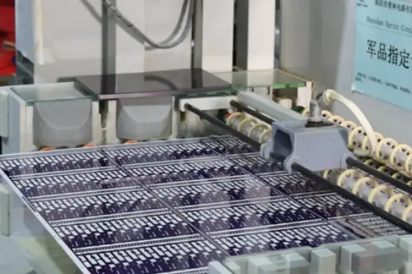
Industrial Automation PCB Reliability: How to Achieve 10+ Years of Stable Operation
In the field of industrial automation, people often pay attention to AI
I have long felt that people harbor a certain misconception regarding the gold-colored connectors found on PCBs. Upon seeing a shiny Gold Finger PCB, they often assume it is crafted from solid pure gold. In reality, these are two entirely different matters.
I have seen people show off their RAM sticks to me, boasting that they are made of “real gold.” That particular luster does indeed tend to create such an illusion. However, you must understand that pure gold is inherently too soft. If these contact points were truly made of pure gold, they would likely deform after just a few insertions and removals.
I recall an instance where I was helping a friend repair his computer; I discovered his graphics card was suffering from poor contact. Upon disassembling it, I found that the so-called “gold” contacts had actually worn down to a whitish color. I later learned that many manufacturers, in an effort to cut costs, compromise on the quality of the plating. Truly reliable manufacturers, however, consistently choose to employ the “hard gold” plating process for these critical components.
Hard gold offers far superior wear resistance compared to standard plating. It is capable of maintaining stable electrical performance even under conditions of frequent insertion and removal—a feature that is particularly vital for industrial equipment. I have handled numerous industrial control motherboards; these machines often run continuously for years on end without ever failing due to contact-related issues.
Of course, cost is also a practical consideration; using hard gold exclusively for every component would indeed be economically unfeasible. Consequently, many consumer-grade products today make compromises regarding plating thickness; nevertheless, the critical signal transmission sections must still rely on this specialized plating to ensure proper conductivity.
I believe that when selecting hardware, one should not be swayed solely by shiny surface aesthetics; rather, one should focus on the specific manufacturing processes employed by the manufacturer. Sometimes, spending a little extra to choose a reputable brand can actually save you a great deal of trouble and provide greater peace of mind in the long run.
I have observed many people falling into common pitfalls when it comes to understanding gold fingers. The design of gold fingers involves far more complexity than simply the thickness of the plating. I recall an instance while debugging equipment where I noticed signal instability. After repeated checks, I finally discovered that the issue stemmed from improper handling of the solder mask layer. That incident taught me that, sometimes, the root of a problem lies hidden within the most fundamental process details.
The “window” design in the gold finger area requires particular care. Improper edge treatment can easily lead to ink peeling; these minute particles can directly compromise contact stability. I make it a practice to incorporate rounded corners at the edges of these windows; while this adds complexity to the manufacturing process, it effectively prevents potential reliability issues during subsequent operation.
Regarding the treatment of internal copper foil layers, many people tend to overlook the impact on electromagnetic compatibility (EMC). During high-speed signal transmission, the copper layer situated beneath the gold fingers can generate parasitic effects. Judiciously removing sections of this internal copper foil—though it may increase costs—is absolutely critical for maintaining signal integrity.
Another frequently overlooked aspect is the layout of surrounding components. I once worked on a project where, in an effort to save space, vias were placed too close to the gold fingers; this resulted in momentary short circuits occurring during the insertion and extraction process. Consequently, I now strictly enforce a rule requiring a sufficient safety clearance between surrounding components and the gold fingers—even if doing so makes the routing layout slightly more complex.
The choice of angle for the gold fingers is actually quite a nuanced matter, as different devices have vastly different requirements regarding the tactile feel of insertion and extraction. I prefer to adjust the angle based on the specific application scenario rather than blindly adhering to standard parameters; after all, user experience remains the ultimate benchmark for success.
These insights have been accumulated through hands-on experience in actual projects; every single detail has the potential to impact overall system performance.
I’ve long felt that many people harbor a misconception regarding the gold-plated contact points found on PCBs: they assume that simply because a contact is gold-colored, it must be inherently durable. In reality, the technical nuances involved are quite fascinating.
I recall an instance where I helped a friend repair a vintage video game console. The gold fingers within the cartridge slot were severely worn down, causing the video output to frequently display “snow” or static. Upon disassembling the unit, I discovered that the early design had utilized only standard gold plating; after just a few dozen insertions and extractions, the underlying base material had already become exposed. Looking back now, had they employed an appropriate “hard gold” plating process back then, the component likely wouldn’t have failed so easily.
The primary advantage of “soft gold” lies in its excellent ductility, making it ideal for applications that require soldering. For instance, certain semiconductor packages require gold wire bonding during assembly, and a material that is too rigid would be prone to fracturing. However, this very softness also implies that it cannot withstand frequent friction—much in the same way that you wouldn’t use a rubber eraser to repeatedly scrub the surface of a precision instrument.
The most extreme example I’ve ever encountered involved expansion cards used in industrial control cabinets; I was told that these cards had to be inserted and removed multiple times *every single day*. The manufacturer specifically opted for a cobalt-hardened gold finish; even after three years, the contact points remain bright and lustrous. In this particular application, had they used soft gold instead, I estimate the unit would have required servicing within just three months.
However, when it comes to hard gold, thicker isn’t necessarily better. An excessively thick plating layer can actually lead to poor contact—particularly in interfaces that require precise alignment. I encountered this exact issue once while modifying audio equipment; the problem was ultimately resolved only after switching to a plating of moderate thickness.
Nowadays, whenever I purchase equipment featuring PCBs with “gold fingers,” I pay close attention to the manufacturer’s process specifications. After all, that seemingly simple golden edge often determines the entire device’s operational lifespan. Some budget products cut corners in this area to save costs; while they may function without issue initially, their true deficiencies inevitably surface over time.
In reality, the surface treatment of metals is much like controlling the heat when cooking: different applications require different recipes. There is no need to blindly pursue the hardest or softest option; the key lies in finding the optimal balance that best suits the specific requirements at hand. This principle applies across a wide range of industries.
I have long felt that many people harbor misconceptions regarding the gold-finger sections of circuit boards. People often focus solely on the thickness and luster of the gold plating itself, while overlooking the critical factors that truly determine the component’s lifespan. In truth, that gleaming golden surface represents merely the outermost layer—a tiny fraction—of the entire connection system.
I have encountered numerous cases where excessive focus on plating thickness led to the neglect of overall design integrity. During a recent equipment test, I discovered that although the gold plating met the standard thickness specifications, contact issues still arose after repeated insertion and removal cycles. A subsequent teardown and analysis revealed that the underlying metal substrate lacked sufficient structural support, causing microscopic cracks to form in the surface plating whenever mechanical stress was applied.
The true determinants of a gold-finger PCB’s durability are often the elements that remain invisible to the naked eye—such as the metal substrate’s elastic modulus, the adhesion strength of the plating, and the structural design of the connector assembly as a whole. Sometimes, in the pursuit of a slimmer device profile, designers may compress the dimensions of the gold fingers; ironically, this can actually reduce the component’s insertion-cycle lifespan. The ideal approach—whenever spatial constraints permit—is to appropriately increase both the contact surface area and the structural robustness.
The physical layout of the gold-finger area on a PCB also demands careful consideration. I generally prefer to distribute the mechanical stress across multiple contact points rather than concentrating it on just a few specific spots. This ensures that even if wear occurs at a particular location, the remaining contact points can still maintain a reliable connection. In practical applications, this design approach indeed significantly extends the service life of the interface.
Regarding the issue of insertion-extraction cycles, I believe that rather than fixating on theoretical maximum limits, it is more productive to focus on proper maintenance practices during daily use. Simple habits—such as keeping the interface clean and avoiding hot-plugging (connecting or disconnecting while powered on)—often yield more tangible benefits than simply chasing ultra-high specifications for the “gold fingers.” After all, even the finest hardware cannot withstand rough handling.
Speaking of the choice of materials for gold fingers, that is indeed an interesting topic. Some manufacturers are now experimenting with incorporating other metal elements into the gold plating layer to enhance performance; this approach can certainly improve specific technical metrics. However, the average user is likely more concerned with stability and compatibility in real-world usage scenarios.
From a repair and maintenance perspective, issues with gold fingers are often caused not by wear on the plating itself, but by damage to the underlying circuitry. This underscores the need to prioritize ease of repair during the design phase—ideally enabling modular replacement of components rather than requiring the replacement of the entire circuit board.
Ultimately, technical specifications serve merely as a reference; a truly excellent design must strike a balance between theoretical performance and practical application scenarios. After all, what users truly require is not flawless laboratory data, but a stable and reliable user experience.
I have long felt that many people harbor misconceptions regarding Gold Finger PCBs. People tend to focus their attention solely on that shiny surface finish. In reality, the critical factors that truly determine a circuit board’s performance are often hidden from view. For instance, the issue of impedance matching is frequently underestimated.
I recall an instance where we were testing a high-speed communication board and discovered that its signal integrity was exceptionally poor. Our initial reaction was to check for contact issues within the connector. However, despite repeatedly swapping out gold finger connectors from several different manufacturers, the problem persisted. We eventually discovered that the issue stemmed from an inappropriate choice of base material, which resulted in impedance discontinuities throughout the entire signal transmission path. That experience taught me a valuable lesson: no matter how perfect the surface finish may be, it remains merely the icing on the cake.
I have observed numerous engineers who, during the design phase, place excessive emphasis on metrics such as plating thickness. While this is undoubtedly important, it is even more critical to consider the synergistic interplay of the entire signal path. Sometimes, in the pursuit of an “ultimate” surface finish, other vital performance metrics are inadvertently compromised.
Many manufacturers today like to tout the specific thickness of the gold plating they employ. However, our experience in practical applications suggests that simply meeting the basic requirements for wear resistance is sufficient. The area that truly warrants focused effort is the optimization of the overall structural design. For example, in high-speed application scenarios, the stability of the base material’s dielectric constant may be far more critical than the thickness of the plating layer. We recently encountered an interesting situation while working on a medical device project. Due to the unique operating environment of the equipment, a standard “gold finger” design approach would have resulted in severe signal attenuation. By subsequently adjusting the substrate parameters and optimizing the routing strategy, we not only resolved the signal integrity issues but also reduced the overall cost.
These experiences have increasingly led me to believe that good engineering design requires balancing a multitude of factors. Solely pursuing the extreme performance of a single parameter can often prove counterproductive—much like cooking, where one must master the heat levels and the precise ratios of ingredients.
Speaking of which, this reminds me of an automotive electronics factory I visited some time ago. The control boards they manufactured were designed to operate in extreme environments. What surprised me most at the time was not the advanced nature of their gold-plating process, but rather the exceptional comprehensiveness of their entire quality control system.
In reality, while the specific requirements for Gold Finger PCBs vary across different industries, they share one common thread: the need for systematic thinking. One cannot simply fixate on a single aspect—such as the surface finish—while neglecting the overall harmony and coordination of the system’s performance.
Looking back at past failures, I’ve realized that most problems stemmed from a failure to properly balance the interdependencies between various parameters. Sometimes, the simplest solution turns out to be the most effective.
I believe the most important attribute for a technical designer is maintaining an open mind. One must not blindly and mechanically apply a solution that succeeded in one domain to every conceivable scenario; every project possesses its own unique characteristics and demands a tailored analysis.
Ultimately, a robust technical solution is one that withstands the test of practical application, rather than remaining confined to theoretical data on paper. This is precisely why I place such a high premium on real-world performance; after all, what the end user truly cares about is stable and reliable operation.
I’ve encountered quite a few engineers who get overly fixated on the gold content of the fingers—acting as if higher purity automatically equates to greater reliability. In truth, this perspective is rather one-sided. The true determinant of a Gold Finger PCB’s performance often lies in the user’s daily insertion and extraction habits; those seemingly trivial actions are, in fact, what ultimately dictate the maximum lifespan of the connector.
I recall a specific instance involving the testing of industrial control boards. Two batches of boards—produced concurrently—had undergone the exact same gold-plating process. Three months later, the batch subjected to frequent “hot-swapping” (insertion and removal while powered on) had already begun to exhibit contact issues, whereas the batch that remained in a fixed, stationary installation continued to perform stably. This experience brought a critical realization to light: we often get too hung up on minute material specifications, yet we overlook the fundamental nature of gold fingers—they are, at their core, consumable components. Even with the thickest possible gold plating, forceful or rough handling during insertion and removal will inevitably accelerate wear and tear.
Consequently, when designing now, I place a much greater emphasis on the mechanical fit and structural compatibility of the components. For instance, one must consider whether the chamfered guides on the connector slot allow the gold fingers to slide in smoothly, or whether the contact pressure is distributed evenly across the contact points. Sometimes, allocating a little extra budget to incorporate a floating connector structure proves far more effective than simply increasing the thickness of the plating. After all, reliability isn’t built merely by “piling on” expensive materials.
I recently worked on a project involving a drone video transmission module that left a deep impression on me. The client initially insisted on using the highest-specification hard gold plating available. However, we suggested reallocating a portion of that budget to connectors equipped with a locking mechanism. The result? For the exact same cost, the connector’s mating cycle lifespan increased by more than threefold. While those gold contacts are indeed crucial, it is often the invisible mechanical design—not the plating itself—that ensures they maintain a stable connection.
Ultimately, the value a hardware engineer brings shouldn’t be confined to material specification sheets; rather, they must view the circuit board as a living, breathing system. While the plating thickness of gold fingers can be calculated mathematically, the tactile feedback during insertion and removal—the “feel” or damping sensation of the interface—often serves as the true litmus test for reliability.
I’ve observed that many people, when dealing with PCBs featuring gold fingers, tend to focus their attention exclusively on the electroplating parameters. In reality, however, the root causes of problems are often latent flaws embedded during the initial design phase. I once inspected a board returned for rework and discovered that a solder pad had been placed too close to the edge of the gold fingers. Consequently, during the production line process, the masking tape failed to seal tightly, allowing the metal plating to bleed into an adjacent area where it didn’t belong.
Such details may seem trivial, yet they directly impact the reliability of the finished product. I recall a client who insisted on laying down a copper pour in the vicinity of the connector interface; this resulted in severe crosstalk interference with high-frequency signals, ultimately necessitating a complete redesign and the creation of a new mold.
What truly gives engineers a headache are those issues hidden deep within the circuit board—specifically, improperly positioned vias. These act like ticking time bombs, potentially causing short circuits or sudden impedance mismatches during the assembly process.
Nowadays, whenever I review a design proposal, I pay special attention to these easily overlooked areas. After all, a robust design isn’t achieved through retrospective patching; it is built by proactively avoiding these pitfalls right from the very start.
Sometimes, the simplest approach proves to be the most effective: maintaining adequate spacing to provide a little manufacturing margin is far more cost-effective than attempting to salvage the situation after the fact.
You might feel that leaving extra space is a waste of precious board real estate, but compared to the catastrophic cost of scrapping an entire production batch, that small concession is a negligible price to pay.
Whenever I see those gleaming, golden-fingered PCBs, I am invariably reminded of the mistakes I made myself when I first entered this field. Back then, I used to think, “What are gold fingers, really? Just a gold-plated area—how complex could they possibly be?” That mindset persisted until the day a board I designed failed miserably; due to plating issues, the gold fingers became so worn down after just a few insertion-extraction cycles that they were rendered unusable. That was when I finally grasped the true intricacies behind this seemingly simple component.
In reality, many people tend to overlook a fundamental fact: when it comes to gold fingers, “thicker is better” is a misconception; rather, finding the *optimal* thickness is what truly matters. I have seen numerous projects where designers, in a blind pursuit of so-called durability, indiscriminately increased the plating thickness. The result was not only skyrocketing costs but also unexpected signal integrity issues. While the thickness of the gold layer does indeed influence the insertion-extraction lifespan, this factor must be evaluated within the context of the specific application scenario. For instance, standard consumer electronics may not require such a thick plating layer at all; in such cases, over-engineering becomes nothing more than a wasteful exercise.
The choice of plating process also requires careful consideration. Some people, upon hearing the term “selective plating,” immediately assume it signifies a high-end, premium process. While it is true that selective plating allows for precise control over the plating quality within the gold finger region, the accompanying increase in process complexity and cost may not be suitable for every project. In some instances, applying an “immersion gold” finish to the entire board proves to be a more economical and practical solution—particularly for applications where the frequency of insertion and extraction is relatively low.
I would like to draw particular attention to one specific detail: the chamfer design of the gold fingers. This may appear to be a minor issue, yet it directly impacts both the tactile feel during insertion and the long-term reliability of the connection. An appropriately angled chamfer ensures smoother insertion into the connector, thereby preventing unnecessary scratching or abrasion of the gold layer. However, this angle must be customized based on the specific connector being utilized; one cannot simply apply generic, standard parameters across the board.
In practical applications, we must also consider the impact of environmental factors on the “gold fingers.” For instance, in high-humidity environments—even if the plating thickness meets specifications—performance may still degrade due to other underlying causes; this necessitates a comprehensive assessment spanning both material selection and process treatment.
Ultimately, the design of “Gold Fingers” tests an engineer’s ability to strike a balance: ensuring sufficient mechanical strength while controlling costs and considering manufacturing feasibility. Finding the optimal solution requires the continuous accumulation of experience through actual projects, rather than simply applying so-called “best practices” in a rote manner.
Sometimes, the simplest solution proves to be the most effective. The key lies in truly understanding the specific usage scenarios and requirements of your product, rather than being blindly led by various technical parameters. This constitutes the core essence of effective Gold Finger design design.
I have encountered many people who oversimplify the plating process for Gold Finger PCBs. They seem to think that merely applying a layer of gold to the edge of the board is all that is required—but in reality, there is a rather interesting set of design choices involved.
Many assume that the thicker the gold layer, the better the performance. This is actually not the case. If you apply a soft metal coating—even one made of pure gold—to an area subject to frequent insertion and removal, it may become worn and scratched after just a few cycles. I once saw a client’s sample board where the slot interface began to suffer from poor contact after being inserted and removed only a few dozen times. It was later discovered that, in an effort to save costs, they had used a standard chemical immersion gold process for the contact points.
A truly reliable approach requires careful consideration of the actual application environment. For instance, expansion cards or test interfaces that undergo frequent insertion and removal require surface treatments utilizing specially formulated metal alloys. Although these materials may contain a lower percentage of gold, they possess greater hardness and durability.
On one occasion, I visited a factory to observe this specific process, and it was quite fascinating: they first applied an intermediate metal layer over the copper substrate, followed by the final surface metal treatment. That intermediate layer serves not only as an isolation barrier but also enhances the structural integrity of the assembly.
In truth, the choice of surface treatment method depends entirely on the specific application. For example, certain devices requiring long-term, stable contact may actually benefit from materials with greater ductility, as this helps accommodate issues related to thermal expansion and contraction.
I believe the most frequently overlooked aspect is the function of that intermediate metal layer; it not only prevents the underlying base metal from migrating upward but also ensures a more robust adhesion for the surface metal layer.
Ultimately, when it comes to this technology, “more expensive” does not necessarily mean “better.” The critical factor is meeting actual requirements; sometimes, spending a little extra to select the right process upfront can save you a great deal of trouble—and cost—in terms of future maintenance. I remember once helping a friend repair a game console; the issue turned out to be that the “gold fingers” in the cartridge slot had worn down excessively. The problem was only resolved after replacing the interface board with one featuring a special protective coating. Since that experience, I’ve paid particularly close attention to such design details.
In fact, many design trade-offs are quite fascinating—for instance, the need to ensure optimal electrical conductivity while simultaneously maintaining mechanical strength, or sometimes having to strike a delicate balance between cost-effectiveness and durability.
In the field of industrial automation, people often pay attention to AI
Ever wonder how your phone maintains a stable signal? It relies on
When selecting components for a security monitoring system, most attention goes to
- 小・中ロット生産のエキスパート
- 高精度PCB製造と自動アセンブリ
- OEM/ODM電子プロジェクトの信頼できるパートナー
営業時間:(月~土)9:00~18:30