
Industrial Automation PCB Reliability: How to Achieve 10+ Years of Stable Operation
In the field of industrial automation, people often pay attention to AI
When it comes to manufacturing circuit boards, many people assume the job is finished the moment the design schematics are handed over to the factory. However, after going through several rounds of trial and error, I’ve come to realize that the true test of one’s expertise lies in the entire sequence of events that follows. This is especially true when you require custom PCB boards with specialized specifications; every single stage—from initial design through to mass production—becomes a constant tug-of-war requiring meticulous attention.
I recall an instance where we were designing a board featuring an integrated RF module; during the schematic design phase, the team was locked in a heated, seemingly irreconcilable dispute. The hardware engineers insisted that signal integrity must take precedence in the layout, while the mechanical engineers adamantly refused to compromise on the constraints imposed by the external enclosure dimensions. In such situations, simply exchanging emails back and forth does absolutely nothing to resolve the actual problem. Eventually, we brought the PCB manufacturer’s engineers directly into a video conference call; the three parties spent two hours poring over the screen together, making real-time adjustments until we finally found a balanced solution. This kind of real-time, cross-disciplinary collaboration proved infinitely more effective than any formal documentation or technical specification could ever be.
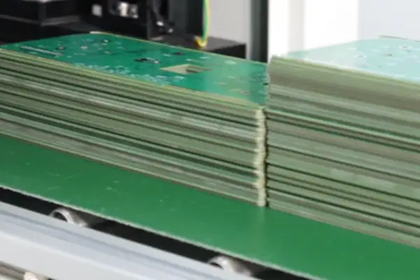
Quality control is another particularly fascinating aspect of this process. On one occasion during an inspection, we noticed that the solder mask on the boards exhibited inconsistent color shading. The manufacturer adamantly maintained that the boards met all IPC standards. However, after pulling out a magnifying glass and comparing the current batch against previous production runs, we were able to clearly identify subtle fluctuations in the manufacturing process. Ultimately, the manufacturer’s technical director flew out personally to visit us; he took us on a tour of their workshop, where we discovered that the temperature zones within their curing ovens were showing signs of aging and degradation. The level of quality improvement achieved through this kind of deep, collaborative engagement is far more substantial and tangible than anything that could be accomplished by simply signing a ten-page quality assurance agreement.
Nowadays, I share a deep, unspoken rapport with the manufacturers with whom I’ve established long-term partnerships. The moment they receive our design schematics, they instinctively know exactly which specific areas require extra attention. In return, we provide them with detailed debugging data collected during our trial production runs to assist them in optimizing their process parameters. On one occasion, they proactively suggested increasing the diameter of a specific via (plated-through hole) from 0.3mm to 0.35mm, explaining that this adjustment would significantly boost the manufacturing yield rate without compromising the board’s overall performance. This kind of trust-based interaction is far more valuable than simply chasing deadlines and nagging for delivery updates.
Ultimately, a good circuit board isn’t merely “drawn up”; it is “honed out” through a painstaking process. From the initial prototype run to final mass production, there are countless details requiring flexible adjustment along the way. Sometimes you might go through three or four iterations just to fine-tune the placement of a single component; other times, you might get into heated arguments over the optimal grounding scheme. Yet, it is precisely these seemingly trivial clashes that imbue the final board you hold in your hands with a true sense of professionalism.
Working on a smart home project recently gave me a deeper appreciation for the fact that many innovative features today rely on specialized PCB fabrication processes. For instance, a board requiring both impedance control and thermal management simply cannot be realized using standard manufacturing processes alone. In such scenarios, whether you can find a manufacturer willing to “get in the trenches” and iterate alongside you—and whether you can establish an efficient communication pipeline—directly determines whether your product can successfully launch on schedule.
In fact, there is a simple litmus test for determining a manufacturer’s reliability: send them your most complex board design for a quote, and observe the depth of the technical questions raised by their engineering team. If they merely provide rote responses regarding lead times and pricing, they likely operate with a purely “contract manufacturing” mindset. However, if they can identify potential design flaws and propose modifications—or even share solutions drawn from similar past projects—then you have found a partner worthy of your long-term trust.
After all, those of us in the hardware world know this much: the traces etched onto a circuit board aren’t just copper foil; they are design concepts imbued with human warmth and intention.
I’ve been pondering something lately: why are more and more people opting for custom PCBs these days? It’s quite an interesting phenomenon.
I recall helping a friend design the mainboard for a small weather station last year. The off-the-shelf boards available on the market were either bloated with unnecessary features—resulting in wasted resources—or simply lacked the required interface compatibility. We went through five different sketches before finalizing the layout; the feeling of arranging every single component in its exact, perfect spot was incredibly satisfying. That experience made me realize that the true allure of customization lies in the ability to shape the very “soul” of a product—precisely in accordance with your own vision.
It’s often a shame to see products where, in an effort to accommodate the rigid dimensions of a standard PCB, designers are forced to create bulky enclosures or compromise on functionality. A truly excellent design should be a seamless, organic whole—integrated from the inside out—much like a tailor crafting a bespoke suit to fit the wearer’s exact measurements.
I particularly enjoy observing the unique and specific PCB design requirements found across different industries. Medical equipment prioritizes absolute stability, whereas consumer electronics place a greater emphasis on compactness. This fundamental difference serves to illustrate precisely why generic solutions can never truly replace the inherent value of a bespoke, tailored approach.
Of course, custom PCBs are not a panacea. If you are merely creating a simple prototype or conducting a small-batch trial run, utilizing off-the-shelf development boards may prove to be the more cost-effective option. The key lies in clearly defining the specific degree of customization your project truly requires.
Nowadays, many teams have begun integrating PCB design into the early stages of product planning—a highly positive trend. When hardware design and industrial design proceed in parallel, the synergy between the two often sparks more innovative and intriguing ideas.
Ultimately, the choice between a custom design and an off-the-shelf solution hinges on the depth of your understanding of the product itself. Once you possess a crystal-clear vision of what you intend to create, the answer will naturally reveal itself.
I feel a surge of excitement every time I receive a newly designed custom PCB. It feels much like unboxing a “mystery box”—brimming with anticipation. Yet, excitement aside, one must never skimp on the necessary due diligence; after all, these boards bear the weight of the entire project’s success or failure.
My standard practice is to begin with a comprehensive “health check” of the board, meticulously inspecting every component for potential issues such as cold solder joints or short circuits. I once encountered a particularly elusive problem: everything appeared normal on the surface, yet the system would inexplicably reboot whenever a specific program was executed. We eventually traced the issue back to an undersized capacitor; its capacitance value was insufficient to maintain stability when the power supply fluctuated. Diagnosing such issues often requires the use of an oscilloscope to observe power supply ripple—particularly during sudden changes in load—as the charging and discharging characteristics of capacitors directly impact system stability. For instance, the moment a processor transitions from sleep mode to full-speed operation, its current demand spikes several-fold; if the decoupling capacitor configuration is inadequate, it will trigger a voltage drop.
The validation phase is the ultimate test of patience, requiring us to simulate various extreme scenarios to put the board through its paces. Alternating high- and low-temperature cycling is considered standard procedure; at times, we even deliberately induce voltage fluctuations or signal interference. While this may sound somewhat brutal, we can only confidently deploy a board for actual use once it has successfully withstood these rigorous trials. We typically employ a climate chamber to conduct thermal cycling tests ranging from -40°C to 85°C, while simultaneously using a programmable power supply to simulate grid fluctuations and positioning high-frequency noise sources around the board to verify its electromagnetic compatibility. On one occasion, during low-temperature testing, we discovered that the startup time of a specific chip fell outside the range specified in its datasheet; this timely discovery allowed us to avert potential risks that would have arisen had we proceeded to mass production.
The most common pitfall during the design phase is being overly idealistic. While theoretical planning on paper may seem foolproof, actual assembly often reveals flaws in the layout that were not adequately anticipated. For instance, we once placed a crystal oscillator in close proximity to a high-power component; the result was a clock signal so severely distorted by interference that it became completely unrecognizable. Subsequently, we established a comprehensive layout checklist, mandating impedance matching for high-frequency signal lines, requiring sensitive analog circuits to be isolated from digital circuits, and stipulating that critical signals undergo shielding. Particularly when board real estate is limited, meticulous attention to these details often proves decisive in determining the overall signal-to-noise ratio of the entire system.
Nowadays, I routinely allocate a 20% margin for potential modifications in my designs; after all, real-world implementation inevitably presents unexpected challenges. On one recent project, the positioning of an interface required adjustment; fortunately, we had preemptively reserved spare pins, allowing us to resolve the issue simply by running a jumper wire. These reserved resources typically include additional test points, unused GPIO pins, configurable resistor networks, and even designated footprints for 0-ohm resistors within critical power supply paths. On another occasion, a client made a last-minute request to add Bluetooth functionality; thanks to our foresight in reserving the necessary antenna interface and chip footprints, we were able to rapidly implement this secondary development.
The most vexing issues are often those intermittent, “soft” failures—glitches that appear and vanish unpredictably. We once had a circuit board that ran flawlessly in the lab for a full week, only to suffer from frequent system crashes once it reached the client’s site. It was only after traveling to the site and conducting an extended period of on-location monitoring that we pinpointed the root cause: instability in the local power grid voltage. Resolving such issues often necessitates long-term monitoring using data loggers; consequently, we have since equipped our critical hardware units with power quality monitoring modules capable of recording parameters such as voltage sags and harmonic distortion. In one particularly memorable instance, we discovered that electromagnetic interference generated by a variable-frequency drive within the client’s factory was coupling into our equipment via the power supply lines.
These experiences have taught me that a truly robust design must not merely satisfy theoretical specifications, but—more importantly—must be capable of withstanding the rigors of real-world operating environments.
With every hardware revision, we make it a point to maintain meticulous records, clearly documenting both the rationale behind each modification and the specific solutions implemented. This accumulated body of knowledge gradually evolves into a comprehensive team knowledge base, enabling new colleagues to avoid many common pitfalls and navigate similar technical challenges with far greater efficiency. We now utilize a version control system to log every modification—including schematic changes, layout adjustments, and BOM updates—and we always attach photos of observed failure symptoms and relevant test waveforms. On one occasion, a new colleague encountered a signal integrity issue with a DDR4 interface; by simply referencing a termination matching solution found in our internal knowledge base, they were able to resolve the problem immediately.
I believe the most captivating aspect of hardware engineering lies in this iterative process of trial-and-error and continuous optimization. Although each design revision entails additional workload, the sense of accomplishment derived from seeing a product become increasingly stable and reliable makes it all worthwhile.
Recently, I’ve been experimenting with simulation software to identify potential issues early in the design phase, which has indeed saved us a significant amount of time during subsequent debugging. For instance, we use SIwave for signal integrity analysis and thermal simulation tools to predict hotspot distribution. On one occasion, a simulation revealed an impedance discontinuity at a specific via; we were able to optimize the design and resolve the issue before sending the board out for fabrication.
However, even the most advanced tools cannot fully replace actual physical testing; after all, the real world is invariably far more complex than any theoretical model. Simulations cannot perfectly replicate every environmental variable—factors such as component batch variations, fluctuations in soldering processes, or even the unique usage habits of different operators can all impact a product’s final performance.
Consequently, I have cultivated a strict habit: I never authorize a design for mass production until it has successfully passed at least three rounds of rigorous physical validation. The first round focuses on basic functional verification; the second covers environmental adaptability testing; and the third involves long-term aging and reliability testing. Each round must be conducted on a minimum of three prototype boards.
This approach demonstrates both a sense of responsibility toward our clients and a deep respect for the integrity of our own work. After all, no one wants their creation to turn into a “ticking time bomb” once it hits the market, right?
While recently perusing product catalogs from various PCB manufacturers, I noticed an interesting phenomenon: they often pile on flashy technical specifications—much like a Michelin-starred restaurant stacks up exotic ingredients on a menu—yet the factors that truly determine a project’s ultimate success or failure are, in fact, the most fundamental design choices. Take, for example, a smart home gateway project our team worked on last month: we initially debated whether to adopt High-Density Interconnect (HDI) technology. Ultimately, however, we opted for a standard multilayer board combined with a well-optimized custom PCB layout; this decision slashed our production costs by 30% and allowed us to deliver the final product two weeks ahead of schedule.
Nowadays, many engineers tend to fall victim to “technological fetishism”—blindly chasing the latest trends simply because they see others utilizing a specific process or technology, without stopping to evaluate whether it truly aligns with their own specific application requirements. I recall visiting an electronics trade show where an exhibitor specializing in industrial sensors proudly showcased their 20-layer PCB design; yet, upon closer inspection, the density and efficiency of their routing layout were actually inferior to those of a simple four-layer board designed by a group of university students exhibiting right next door. This kind of over-engineering is particularly common in startups—it’s like insisting on installing a racing engine in a commuter scooter.
When it comes to high-frequency circuits, I tend to favor a conservative strategy. The last time I helped a friend debug a drone’s video transmission module, we went through boards from three different suppliers before realizing the problem lay in something as simple as impedance matching. Manufacturers who market themselves as specialists in the RF/EMI field are quick to recommend exotic materials at the slightest provocation; yet, with rigorous calculation, standard FR4 boards can perform just as stably at frequencies below 6 GHz. Sometimes I feel this industry needs more pragmatists—people focused on practical application—and fewer “spec sheet warriors.”
Regarding future trends, I actually hold a different view. Everyone is currently hyping up rigid-flex PCBs, but our lab has disassembled numerous returned and defective devices, and we’ve found that the flexible interconnects are actually high-failure zones. In the automotive electronics sector, there has recently been a shift back toward a design scheme dominated by rigid boards with connector-based transitions; after all, reliability isn’t something you can simply “stack up” using fancy new materials. I’ve seen too many teams get bogged down chasing after esoteric technologies, only to neglect fundamental engineering tasks—such as proper power supply routing.
Truly good design should be like a master craftsman working with wood: you must first thoroughly understand the inherent nature of the material before making your first cut. When I recently redesigned an audio decoder, I deliberately chose the most standard double-sided PCB process; by optimizing the grounding strategy, I was able to achieve a signal-to-noise ratio of 110 dB. As you advance in this field, you eventually realize that mastering cutting-edge technologies is actually easier than mastering the *restraint* to know when—and when not—to use them.
I’ve noticed a common pitfall many people fall into when commissioning custom circuit boards: they assume they can simply dump all their requirements onto an engineer and be done with it. In reality, the truly critical step is for *you* to first clearly define exactly what it is you need. Often, the requirements we *think* we have are merely surface-level symptoms, potentially masking deeper, more practical underlying issues.
For instance, I once helped a friend design a small sensor board. Initially, he simply stated that he needed it to measure temperature and humidity. However, as we talked it through, I discovered that what he *really* needed was a device capable of operating continuously outdoors for three months without recharging—a requirement that completely transformed the design approach for the power supply section. Had we proceeded based solely on his initial request, we almost certainly would have ended up having to rework the entire board.
The biggest nightmare in custom PCB design is a change of mind midway through the process. My personal habit is to spend half a day with the client—before I even start designing—to thoroughly map out the application scenarios. I don’t just ask, “What functions do you need?” Instead, I seek to understand where the board will ultimately be installed, what its surrounding environment will be like, and who will be operating it. These details are often far more important than technical specifications alone.
I recall a client who insisted on pursuing the highest-performance chipset available; as a result, their budget went severely over limit. Later, they realized that a mid-range chipset would have fully met their actual needs—and saved them the hassle of complex thermal management design. Sometimes, we get so caught up in comparing technical specs that we lose sight of the product’s intended positioning.
Now, whenever I receive a new request for a custom design, I start by asking a few seemingly simple questions: What is the device’s primary function? What are the most common usage scenarios the user will encounter? Is there any potential for adding new features in the future? These questions may seem basic, but they help us avoid a great many detours.
Good design isn’t about simply piling on the most high-end components; it’s about finding the optimal balance point. It’s like a tailor making a suit: they must first understand the wearer’s lifestyle and habits, rather than just focusing on using the most expensive fabric available.
After years of designing circuit boards, I’ve come to a realization: many people view PCBs far too simplistically. They assume it’s just a matter of drawing a schematic, handing it off to a factory, and waiting for the finished product to arrive. In reality, the success or failure of a board is often determined by those invisible details.
I remember one instance where a client insisted on cutting costs by downgrading a four-layer board to a two-layer board. The entire batch of products subsequently failed, and we later discovered the root cause was insufficient current-carrying capacity. That lesson taught me that when designing a circuit board, you must first clearly define its functional requirements rather than blindly chasing the lowest price.
Nowadays, whenever I design custom circuit boards, I pay particular attention to copper foil thickness. Many people assume this parameter is “close enough,” but in reality, a difference of just a few tenths of a millimeter can yield vastly different results. For instance, in high-power devices, thin copper foil compromises thermal dissipation, directly shortening the lifespan of the components. Sometimes, you even see the circuit traces turn slightly yellow from overheating—a sight that is truly disheartening.
The most extreme case I’ve ever witnessed involved someone attempting to run high currents through a standard PCB; the copper foil actually burned right through. Once they switched to a board featuring thickened copper foil, the problem was instantly resolved. This incident drove home the point that you simply cannot compromise on material selection; where thick copper is required, you absolutely must not skimp.
Another subtle detail is the flatness of the board material itself. To save costs, some manufacturers produce boards that are excessively thin, leading to warping and bending issues during the surface-mount assembly process. I now insist on a minimum board thickness of 1.6 millimeters; while it adds slightly to the cost, it saves us from countless headaches down the line.
Ultimately, after working in this industry for a while, you realize that the true difference between a high-quality board and a poor one lies precisely in these subtle details. Sometimes, simply adding a few millimeters of thickness or switching to a different copper foil specification can elevate the reliability of the entire board to a whole new level; these are the kinds of insights one only gains after stumbling through—and learning from—past pitfalls.
Having designed custom PCB boards myself for years, my biggest takeaway is this: the design process cannot be rigid. Many people start out aiming to plan every single detail flawlessly right from the get-go—mapping out every trace, positioning every component, and placing every test point—as if they could draft a perfect schematic in a single pass. But in reality, that’s simply not how it works. I remember one instance where I spent two months wrestling with a complex RF board; the design alone went through seven or eight revisions.
You never know what kind of curveballs the manufacturing stage might throw at you. Once, I sent my Gerber files to a manufacturer, only for them to report back that the spacing in the solder mask layer was too tight—beyond the precision capabilities of their machinery. Had I stubbornly pushed ahead with the original plan, the entire batch of boards would have been scrapped. I learned my lesson: now, whenever I draft a layout, I deliberately incorporate several areas of redundancy.
For instance, I might lay down an extra patch of copper pour next to a power module, or reserve space for a few extra vias near critical signal lines. In the initial design phase, these elements might appear superfluous.
However, when the manufacturer reports that a certain impedance needs fine-tuning, or when testing reveals the need to add a filtering capacitor, that reserved space becomes a lifesaver. A motor driver board I worked on recently was saved precisely because I had preemptively added a few extra pads next to the MOSFETs.
Later, the client made a last-minute request to add a current-sensing resistor. Thanks to that existing spare space, we were able to resolve the issue simply by running a few jumper wires. Some might view this kind of “white space” as a waste of board real estate. In truth, it is the most efficient approach of all.
After all, you cannot possibly anticipate every conceivable scenario while sitting at your computer. Those legendary cases of “first-time success” usually fall into one of two categories: either the board design was extremely simple to begin with, or the story conveniently omits the hidden rework and troubleshooting that actually took place.
Now, before submitting my design files, I take two specific steps: First, I run simulations on extreme-case scenarios using specialized software. Second, I deliberately send the schematics to two different manufacturers—each with varying levels of technical capability—specifically to invite their critiques. The conflicting suggestions they offer often serve to expose potential underlying issues. This seemingly contradictory process proves far more effective than any standard checklist.
A recent industrial controller project serves as a prime example: the first manufacturer claimed the traces were too thin, which would compromise production yield; the second complained that there were too few test points, making inspection difficult. By finding a compromise and incorporating modifications based on their feedback, we ultimately produced a far more robust and reliable version of the board.
Ultimately, designing custom circuit boards is much like doing fine carpentry: no matter how precise your blueprints may be, you must always leave a little extra material—some “wiggle room”—for the final sanding and finishing touches. I made a rather amusing mistake when I designed and built my very first custom PCB. At the time, I figured that since it was a double-sided board—meaning traces could run on both sides—I could just lay out the components haphazardly. Consequently, I discovered that the signal lines needing to cross between layers had to rely on a dense array of vias for interconnection. It was only later that I realized these seemingly insignificant little holes actually determine the stability of the entire circuit. During one testing session, a single via with a poor connection caused the system to fail intermittently; it took me two whole days of troubleshooting to finally pinpoint the problem.
What many people tend to overlook is that a via is not merely a conductive channel; it also influences the mechanical integrity of the circuit board. I’ve seen vintage circuit boards in industrial equipment that have been in service for over a decade; the connection points utilizing metallized through-holes remain robust, whereas the surface-mount components are often the first to suffer from solder joint failure. The reliability afforded by this physical penetration is particularly evident in high-vibration environments—after all, the component leads physically pass through the substrate and are fully encapsulated by solder.
Although High-Density Interconnect (HDI) technology is currently in vogue, I still deliberately incorporate through-holes when designing power modules or interface circuits. This is especially critical for high-current paths, where utilizing multiple parallel vias can effectively reduce impedance and mitigate heat generation. When I was recently designing a motor driver board, I arranged two rows of slightly larger-diameter through-holes around the MOSFETs; the resulting heat dissipation was significantly superior to relying solely on copper traces.
In fact, one can often gauge the quality of a circuit board’s design by examining how its vias are implemented. Shoddy manufacturing processes can result in uneven copper plating on the hole walls—or even completely compromised holes—whereas a sophisticated fabrication process transforms these vertical channels into integral elements of a three-dimensional routing scheme. I gained an even deeper appreciation for this “three-dimensional mindset” recently while experimenting with blind vias to create localized high-density connections on a four-layer board; a circuit board is never merely a two-dimensional work of art, but rather a three-dimensional architectural structure.
Sometimes, I feel that the most captivating aspect of electronic design lies precisely in the meticulous selection of these microscopic details. Once you realize that every single via serves as a bridge connecting disparate signal layers, you begin to prioritize factors such as positional precision and electrical characteristics. These minuscule channels—perforating the very substrate of the board—are the conduits for the system’s most fundamental communication requirements; their importance is every bit as significant as that of the flashy components arranged across the board’s surface.
I often get the sense that many people harbor certain misconceptions regarding the process of designing custom PCBs. Whenever I see someone constantly tweaking a ready-made development board, I feel it’s a real shame—it’s like being perfectly capable of building your own house, yet choosing instead to live in a generic model home designed by someone else.
When I first started out in circuit design, I went down a few wrong paths myself. Once, in a rush to meet a project deadline, I simply copied an existing schematic verbatim—only to discover later that a critical chip had been discontinued three months prior. Another time, I helped a friend modify a drone flight controller board; he insisted on using a standard off-the-shelf board and simply cutting it down to size, but the resulting signal interference was severe. We ultimately had to redesign and fabricate a custom four-layer PCB to resolve the issue.
What truly fascinates me is the schematic design phase—much like outlining a novel before you start writing. You can let your imagination run wild, experimenting with all sorts of circuit topologies. Sometimes, a new structural idea will strike me in the middle of the night, and I’ll immediately hop out of bed to sketch it down on paper. The thrill of such creativity is something that pre-made modules can simply never provide. For instance, trying to replace traditional resistive voltage dividers with current mirrors, or designing symmetrical differential pairs to suppress common-mode noise—this degree of freedom ensures that every circuit bears the unique imprint of its designer.
I remember working on a smart planter project last year where I got stuck on the sensor circuitry for two weeks. Eventually, I printed out the schematic, taped it to the wall, and stared at it intently for three days straight. Suddenly, it hit me: the problem lay in the bias voltage. That moment of sudden epiphany was far more exhilarating than any ready-made solution could ever be. I realized that the reference voltage for the soil moisture sensor required millivolt-level precision, whereas the LDO (low-dropout regulator) I had initially selected suffered from excessive temperature drift, causing the readings to fluctuate periodically. These kinds of practical, real-world details are things you would never be told about when simply using off-the-shelf modules.
Nowadays, many engineers rely too heavily on simulation software. However, I prefer to build a physical prototype board to verify my designs before finalizing them; after all, actual circuits always possess subtle characteristics that simulations simply cannot capture. It’s just like cooking: you can’t rely solely on the recipe; you have to taste the food yourself. This is especially true for parasitic parameters in power circuits, or electromagnetic compatibility issues at high frequencies—only by taking actual measurements with an oscilloscope can you detect potential issues like ringing or ground bounce.
As for the issue of custom design costs, I believe one must look at the long-term value. Just last week, I received a batch of newly fabricated motor driver boards. Although they cost 30% more than standard off-the-shelf boards, they saved us the hassle of subsequent modifications. Furthermore, by optimizing the placement of the heat dissipation vents, we anticipate doubling the lifespan of the boards—a form of intangible return on investment that is difficult to quantify solely in terms of unit price. For instance, by reducing the area of the MOSFET driver loop by 60%, the resulting improvement in energy efficiency—driven by reduced switching losses—can recoup the additional PCB manufacturing costs within just one year.
What I dread most is encountering teams that skip design discussions just to rush a deadline. During a project review last month, I discovered that one team had—astonishingly—routed both digital and analog power planes on the same PCB layer; consequently, the entire first batch of boards was rendered useless. In reality, spending an extra couple of days optimizing the layout would not have delayed the schedule at all. We measured digital clock harmonics coupling through the power plane into the analog front-end, causing periodic glitches in the ADC sampling values—a fundamental error that could have been easily avoided through simple power plane partitioning.
Sometimes, designing custom PCBs feels a bit like playing Go: you must not only consider your current move but also anticipate the next three to five moves ahead. For example, when selecting components, you shouldn’t just look at the technical specifications; you also need to factor in the supplier’s supply stability. This kind of practical experience is often far more critical than mere proficiency with software tools. I once selected a rather obscure operational amplifier; although its electrical parameters were perfect, it had a lead time of six months. I eventually switched to a pin-compatible alternative model while reserving space for a compensation circuit—that kind of flexibility is, to me, the very essence of good design.
I always keep three of my own failed prototype boards on my desk—not to show off, but to serve as a constant reminder that every single detail deserves meticulous attention. This is especially true in high-frequency circuits, where seemingly trivial adjustments to trace routing can result in performance differences spanning several orders of magnitude. For instance, on one particular board, simply because the trace connecting the crystal oscillator was 3mm longer than the ideal path, the communication bit error rate skyrocketed by two orders of magnitude. Lessons learned this way are far more profound than anything found in a textbook.
Recently, while mentoring some newcomers, I noticed they were always in a rush to jump straight into the PCB layout phase. I make them start by hand-sketching the schematics instead; this “old-school” method—though seemingly tedious—actually forces them to truly understand the flow of current at every single point in the circuit. After all, a great design is never merely the product of blindly stacking together various software tools. I require them to annotate the expected voltage waveforms at every node and explain the charging and discharging paths of the decoupling capacitors; this kind of foundational training cultivates an intuitive grasp of the fundamental physics underlying the circuit.
I’ve always felt that the most exciting part of electronics design is watching your ideas transform into tangible physical objects. Custom PCBs serve as the bridge that brings abstract concepts down to earth—a sensation that feels particularly real when you are physically inserting components into those through-holes with your own hands.
I recently helped a friend rework an old radio project. We initially thought we could just get by using a standard, off-the-shelf development board. However, we soon discovered that the board’s tiny, densely packed solder pads simply couldn’t withstand the physical stress of frequent debugging and component swapping. When I decided to design my own circuit boards, I made a point of reserving specific locations for through-holes to accommodate critical components. Although surface-mount technology is now ubiquitous, there are still situations where this robust method of physical connection remains essential.
I recall a testing session where I discovered a cold solder joint on a chip pin; I was so frustrated I nearly threw the entire board away. Later, I added a reinforcing through-hole on the underside of the board, threaded a copper wire through it, and soldered it in place—and just like that, the problem was solved. This “old-school” workaround might not seem particularly high-tech, but it certainly gets the job done. It reminds me of embedding steel rebar into load-bearing walls during home renovations—it might seem like overkill at the time, but in a critical moment, it’s what holds the entire structure together.
Nowadays, some designs blindly prioritize miniaturization while overlooking actual real-world usage scenarios. For instance, automotive electronics are frequently subjected to vibration and temperature fluctuations; relying exclusively on surface-mount components in such environments carries a significant degree of risk. I’ve made it a habit to reserve space for through-holes in the power supply section and near interface connectors; even if those holes ultimately go unused, it’s still far preferable to having to run “flying wires” to patch up a problem after the fact.
I once encountered a drone flight controller design where the gyroscope chip was positioned over a suspended, unsupported section of the board. Consequently, during flight, resonance caused significant data drift. They subsequently added through-holes at the four corners of the board, using screws to firmly anchor it to the drone’s frame; the stability improved dramatically almost immediately. It is precisely these kinds of minute details—rather than simply stacking up high-end components—that often have the greatest impact on a product’s actual performance.
Whenever I receive a prototype batch of a new board, the moment I look forward to most is tearing open the shipping package. Catching the scent of the flux and visually inspecting every single via to ensure light passes through gives me a profound sense of satisfaction—the kind of grounded fulfillment a traditional artisan might feel. Although modern EDA software can now automatically optimize routing layouts, I still prefer to manually fine-tune the placement of vias along critical signal paths. That sense of direct control is something that simply cannot be replicated by clicking an “auto-route” button.
Some might dismiss through-hole technology as obsolete, but I view it much like the traditional mortise-and-tenon joinery used in fine woodworking. Surface-mount technology is akin to using glue—quick and convenient—whereas through-holes represent a genuine, physical interlocking bond. It is the interplay between these two approaches that allows us to create products that are both elegant in design and robust in reliability. After all, truly excellent design isn’t about showing off technical prowess; it’s about ensuring that every single design choice stands the test of time.
Recently, while experimenting with a hybrid approach—combining blind vias with through-holes on a four-layer PCB—I stumbled upon an interesting observation. Although blind vias do indeed save space, they make it virtually impossible to perform touch-up soldering or repairs from the underside of the board. Consequently, I decided to switch all of my test points back to standard through-holes; while this did result in a slightly larger board footprint, it more than doubled the efficiency of the debugging and troubleshooting process. It is precisely this kind of pragmatic trade-off that lies at the very heart of effective engineering design. Sometimes, gazing at a circuit board packed with components reminds me of my childhood days spent disassembling old appliances. Those sturdy through-hole pins remained rock-solid even after twenty years of use, whereas a modern smartphone motherboard might suffer from solder joint detachment the moment it hits the ground. Technological advancement is undoubtedly crucial, yet amidst the fast-paced nature of modern industry, the value of certain traditional craftsmanship is being rediscovered.
Ultimately, the choice of technology depends on the kind of product you aim to create—whether you prioritize extreme thinness and lightness, or place a premium on maintainability. There is no single “right answer”; what matters is clearly understanding the trade-offs associated with each choice. This distinction, perhaps, is what separates a true engineer from a mere assembly worker.
Over my years of working with circuit boards, I’ve gradually noticed an interesting phenomenon: whenever the topic of “Custom PCB Boards” arises, many people instinctively assume that the more layers a board has, the more sophisticated it must be. In reality, the matter is not quite so absolute.
I’ve handled numerous projects that were successfully executed using nothing more than simple double-sided boards. Sometimes, clients would approach me with complex design requirements; after lengthy discussions, we would discover that by simply optimizing the routing layout, a double-layer structure actually proved to be the more suitable solution. The key lies in truly understanding how current flows and how signals propagate.
When it comes to conductive performance, I pay particular attention to the choice of board material. The impact that different substrate materials have on high-frequency signals can vary by several orders of magnitude. I once assisted an audio equipment manufacturer in revising a design; they had originally planned to use a four-layer board, but we later discovered that by switching to a double-sided material with a more stable dielectric constant, the resulting audio quality was actually superior.
Through-holes are truly a love-hate affair for me. I’ve seen far too many novice designers indiscriminately cramming in vias, only to end up compromising the mechanical integrity of the entire board. The correct approach is to place vias only where they are absolutely necessary, and to strictly avoid them where they are not. I recall an instance while debugging a motor driver board where, due to the accidental placement of a few vias directly beneath a heat sink, the thermal resistance distribution became uneven—rendering the entire batch of boards completely useless.
Nowadays, I get a headache whenever I see designs that blindly chase after multi-layer boards. Just last week, a client insisted on using a six-layer board for a smart switch; I couldn’t help but ask him if he intended to run a full-blown operating system on it. Ultimately, we switched to a sensible double-sided layout, which not only slashed production costs by 40% but also resulted in even more impressive performance metrics.
A truly excellent design isn’t defined by the number of layers it contains, but rather by whether every single via is truly necessary and whether every single trace is utilized to its maximum potential. Sometimes, the simplest double-sided board structure serves as the ultimate test of a designer’s true mastery. I’ve recently been working on an IoT sensor project. Initially, the client insisted on a four-layer PCB, but after redesigning the layout, I realized that a two-layer structure was entirely sufficient—and it even freed up space to accommodate a battery. This pragmatic, context-specific approach to design is far more meaningful than simply stacking layers for the sake of it.
I recently chatted with several hardware engineering peers and noticed an interesting phenomenon: nowadays, whenever people discuss PCB design, they tend to focus exclusively on SMT processes and technical specifications, often overlooking fundamental design principles. For instance, when our team was developing an industrial control cabinet last year, everyone initially recommended a high-density SMT solution. However, during the testing phase, a connector came loose three times while subjected to vibration. We subsequently switched to custom PCBs featuring reinforced through-holes—routing the connector pins directly through the board and soldering them on the reverse side—and the failure rate immediately dropped to zero.
In reality, superior manufacturing isn’t about boasting flashy technical specs; it’s about understanding how to apply the right technology in the right context. I’ve encountered numerous suppliers who brag about the sophistication of their production lines, yet their quality control systems actually apply looser inspection standards to through-hole assembly than they do to SMT. During one inspection, I casually flexed the edge of a board near a through-hole pad and discovered a hairline crack in the copper plating. In a high-temperature, high-humidity environment, such a defect acts like a ticking time bomb.
Truly reliable suppliers, conversely, take the time to discuss the underlying design logic behind through-holes—for instance, explaining why a specific power module *must* utilize through-hole mounting rather than SMT. They might even present cross-sectional diagrams of holes with varying diameters to demonstrate minute details like the uniformity of the copper plating. Many smaller manufacturers today cut costs by reducing the copper plating thickness in through-holes to the bare minimum; while this might pass short-term testing, what happens five years down the road?
During a recent visit to a factory that supplies medical equipment manufacturers, I observed their “burn-in” lab, which was stacked with boards undergoing various forms of extreme stress testing. I noticed that the most durable boards were, surprisingly, the ones utilizing—what might appear to be—old-fashioned through-hole technology. A veteran engineer pointed to a board and explained, “Look closely: we’ve deliberately designed reinforced rings around these vias. During vibration testing, the mechanical stress is effectively distributed across the entire surface of the board.” That kind of practical insight simply cannot be generated by simulation software alone.
Sometimes, selecting a manufacturing process is akin to choosing the right tool for the job: if a situation clearly calls for a hammer, attempting to use a screwdriver—no matter how exquisitely crafted—is utterly futile. This is particularly true for power supply and connector interfaces, where the mechanical stability provided by through-hole technology remains an advantage that SMT simply cannot replicate. While it is true that many chip packages are becoming increasingly miniaturized these days, the designs that truly hold up under extreme conditions are still those that steadfastly anchor critical components directly to the board.
I increasingly feel that the true test of a team’s professionalism lies in whether they know to say—in the appropriate context—that “through-holes are absolutely necessary here.” This is not a sign of conservatism, but rather a demonstration of respect for the laws of physics. After all, a circuit board is ultimately destined to function in the real world, not to sit forever in a display case within a climate-controlled laboratory.
Over my years of designing circuit boards, I’ve noticed a rather interesting phenomenon: when people receive custom PCBs, they tend to fixate on the flashy features while overlooking the most fundamental elements—such as the tiny drilling process. Yet, hidden within this seemingly simple step lie a great many technical nuances.
I recall an instance where I was helping a friend modify a power supply module. He was obsessed with achieving the absolute maximum routing density, pushing the spacing between several critical signal vias to their absolute limit. The moment I saw the schematics, I shook my head; with such minuscule spacing, a standard mechanical drill bit would inevitably cause the board material to delaminate. We eventually switched to laser drilling—which significantly increased costs—but the resulting boards were far more stable. Sometimes, “more precise” doesn’t necessarily mean “better”; it all depends on the actual requirements of the application.
Speaking of which, I must mention the importance of selecting the right board material. The ubiquitous FR4 material we commonly use is prone to deformation in high-temperature environments, which can lead to misaligned drill holes. I once worked on a batch of boards for high-temperature testing equipment that had to be scrapped entirely due to this very issue. We eventually resolved the problem by switching to a substrate with a higher Tg (glass transition) value, combined with controlled-depth drilling. Looking back now, I realize that behind those seemingly simple technical parameters lie a wealth of hard-won lessons and experience.
Thickness control is another easily overlooked aspect. I’ve seen instances where people, in an effort to cut costs, tried to compress an 8-layer board design into a 6-layer stackup. The result was that the internal circuit traces became severely distorted and squeezed together during the lamination process—not to mention the complications this created for specialized processes like back-drilling. When the layer thickness specifications don’t match the design, there isn’t even an opportunity to salvage the board through rework. Consequently, before submitting any board design for fabrication these days, I meticulously verify the compatibility between the copper thickness and the dielectric layer specifications.
In reality, the longer you work in this field, the more you realize that the true determinants of a finished product’s quality are often the most fundamental manufacturing processes. It’s like building with LEGOs: if the foundation is crooked, no matter how intricate or sophisticated the structure you build on top, it’s all for naught. Sometimes, when clients approach me with highly complex design proposals, I actually advise them to simplify the structure first—to ensure the precision of every single drill hole is absolutely spot-on—before we even begin to discuss the more advanced features.
I believe that for many people, the understanding of custom circuit boards remains largely superficial. Last year, while designing an audio processor for a friend, I observed an interesting phenomenon: although the current market trend favors 6-to-8-layer multilayer board designs, our actual testing revealed that a 4-layer structure offered superior stability—making it a far more suitable choice for small-to-medium-scale projects.
That experience prompted me to re-evaluate my approach to board material selection. At the time, we experimented with substrates from several different suppliers and discovered that materials boasting “premium” technical specifications would often exhibit subtle deformations during the actual soldering process. This realization taught me that blindly chasing technical benchmarks can be a misguided approach; the true key lies in identifying a solution that is perfectly tailored to the specific requirements of the intended application. Take the field of automotive electronics, for instance; I’ve seen far too many teams blindly stacking layers upon layers. In reality, many in-vehicle devices simply don’t require such complex structures; a four-layer board, combined with an appropriate thermal design, is sufficient to meet most requirements. On the contrary, over-engineering can introduce additional risks of failure—a point that becomes particularly evident in high-vibration environments.
I recently encountered a fascinating case: an industrial controller manufacturer insisted on using a double-sided board design reinforced with stiffeners. Their products have been operating stably in harsh environments for seven years running. This example demonstrates that, sometimes, the simplest solution proves to be the most reliable; after all, the fundamental purpose of a circuit board is to serve a function, not merely to show off technical prowess.
Speaking of trends in new materials, I actually feel that the industry’s current obsession with high-frequency laminates is a bit excessive. Unless you are working on specialized applications—such as communication base stations—standard multi-layer boards are perfectly capable of handling the vast majority of scenarios. What truly matters is customizing the copper thickness based on actual current loads and thermal requirements, rather than blindly chasing after the latest so-called cutting-edge technologies.
I have always believed that good circuit design should resemble a meticulously tuned mechanical watch—every component working in perfect harmony. An excessive pursuit of technical specifications can actually throw a design off balance—a pitfall that becomes particularly apparent when dealing with high-density routing. Sometimes, taking a step back to opt for a simpler architecture can actually yield superior overall performance.
The true test of an engineer’s skill lies in finding the optimal balance between cost constraints and performance requirements. I’ve seen too many projects go over budget in pursuit of unnecessary technical metrics, only for the final product to fail to demonstrate any tangible value commensurate with that investment. Ultimately, excellent circuit board design should ensure that technology serves the function—rather than allowing technology to dictate the design.
Whenever I see design proposals cluttered with the latest buzzwords, I’m reminded of the working methods of the veteran engineers I encountered early in my career—engineers who could craft astonishingly stable products using nothing more than the most basic board materials. This pragmatic design philosophy feels particularly precious in our current era, which often seems obsessed with chasing after technical gimmicks.
Perhaps we should focus more on how to ensure our circuit board designs resonate deeply with their specific application scenarios, rather than getting trapped in the vicious cycle of a “specifications arms race.” After all, even the most advanced technology must eventually be grounded in practical application; a design that can truly stand the test of time is, in the end, the only truly good design.
Whenever I look at those off-the-shelf development boards, I always feel like something is missing. They remind me of a standard fast-food combo meal—they might fill your stomach, but they’ll never quite capture that unique, soulful flavor of your grandmother’s home cooking. Having worked on numerous hardware projects, I’ve found that the truly fascinating part often begins the moment you draw that very first line.
I recall helping a friend—who works in smart agriculture—modify a humidity sensor last year; the off-the-shelf module he was using kept suffering from interference out in the fields. We completely redesigned the PCB layout, isolating the signal processing section into its own separate zone. As a result, the false alarm rate dropped by a staggering 80%. It is precisely this kind of targeted adjustment that constitutes the true value of customization.
Many people assume that a custom PCB simply involves swapping a component package or adding a few extra connectors, but it is actually far more complex than that. It is akin to solving a multi-dimensional mathematical problem, requiring you to simultaneously consider signal integrity, thermal management, mechanical structure, and even the ease of future maintenance. I once designed an industrial control board where I overlooked the height of a single connector; that oversight nearly forced us to completely re-tool the enclosure mold.
Nowadays, some teams rely too heavily on automated routing tools. While machines can certainly save you time, they can never replace an engineer’s judgment. For instance, decisions regarding the routing of high-frequency signal lines or the segmentation of analog and digital ground planes—these are the subtle details and trade-offs that truly demonstrate one’s technical expertise. I make it a habit to manually fine-tune critical areas; although it might add an extra two hours to the process, it saves me from a heap of headaches down the road.
Speaking of customization, the most satisfying aspect is the ability to practice “subtraction” based on actual requirements. Many generic boards on the market are crammed with unused features for the sake of broad compatibility. When designing your own board, however, you can strip away all the redundancy; sometimes, this allows you to shrink the board’s footprint by a third, bringing the overall cost down along with it. The last time I designed a core board for a portable device, we went so far as to remove even the unnecessary solder pads—after all, we knew we would never, ever use those specific interfaces in the product’s lifetime.
Of course, customization isn’t a universal panacea. For low-volume projects, it can indeed be a drain on resources; however, once you scale up production, the BOM cost savings on each individual board become substantial. More importantly, you gain complete control over component selection, allowing you to opt for more reliable materials or specialized coatings better suited for harsh operating environments.
I’m currently working on a high-temperature-resistant PCB project for a client who needs the device to operate continuously right next to a boiler room. We tested three different substrate materials before ultimately settling on an aluminum-based substrate; although slightly more expensive, its thermal dissipation performance proved to be exceptionally robust. This kind of deep-dive optimization—tailored specifically to a unique operating scenario—is the very essence of customization.
Ultimately, hardware design is much like bespoke tailoring: off-the-rack sizes will never fit quite as perfectly as a garment tailored specifically to your measurements. When you hold that circuit board in your hands—a board born specifically for *your* project, with every single trace reflecting a deep understanding of your requirements—the sense of accomplishment you feel is something that simply cannot be bought by purchasing a standard, off-the-shelf product.
In the field of industrial automation, people often pay attention to AI
Ever wonder how your phone maintains a stable signal? It relies on
When selecting components for a security monitoring system, most attention goes to
- 小・中ロット生産のエキスパート
- 高精度PCB製造と自動アセンブリ
- OEM/ODM電子プロジェクトの信頼できるパートナー
営業時間:(月~土)9:00~18:30