
Industrial Automation PCB Reliability: How to Achieve 10+ Years of Stable Operation
In the field of industrial automation, people often pay attention to AI
Every time I see those chips boasting GHz performance parameters, I wonder how much of those numbers can actually be transmitted to the other end of the system. Choosing the right high-speed PCB manufacturer is never about how high a frequency specification they can handle, but about how they understand the subtle changes in current flow within conductors.
I recall a strange problem our team encountered while designing a data processing module. Simulation results were ideal, but actual testing revealed severe signal distortion. We later discovered the issue stemmed from the dielectric constant provided by the board supplier fluctuating beyond expectations at different frequencies. These subtle differences, often overlooked in datasheets, have a significant impact on actual performance. For instance, in the millimeter-wave band, a 0.1% deviation in dielectric constant can lead to accumulated phase errors, causing beam pointing deviations in the array antenna. Such latent problems require manufacturers to utilize vector network analyzers for multi-frequency scanning verification, rather than simply relying on the nominal values provided by the material supplier.
The true test of a manufacturer’s skill often lies not in their ability to process extremely fine linewidths, but in their mastery of material properties. The high losses of ordinary FR4 material at high frequencies can render even the most meticulously designed components useless, while certain specialty resin substrates, though more expensive, maintain stable electrical characteristics. This choice requires a trade-off based on the specific application scenario. For example, in automotive radar modules, using a low-loss PTFE substrate increases costs by 30%, but ensures a 15% improvement in 77GHz signal transmission distance. This trade-off directly relates to the system’s core competitiveness.
Impedance control may sound like a standard technical entry, but it’s actually about how signals maintain their shape along the path. I’ve seen too many cases where tiny deviations in the lamination process caused characteristic impedance drift, ultimately rendering entire batches of boards unusable. Good manufacturers keep impedance tolerances within 5%, requiring precise control at every stage from etching to lamination. Modern HDI boards also employ real-time impedance monitoring systems, adjusting etching parameters through feedback, similar to APC control in semiconductor processes, which is crucial for maintaining batch consistency.
Another easily overlooked detail is via design. They’re like tollbooths on a highway—necessary yet potentially bottlenecks. Parasitic capacitance generated when high-frequency signals pass through vias slows down edge rates. Simple through-holes are no longer sufficient; back-drilling or laser microvia technology is now preferred to reduce stub effects. The stability of these processes directly determines the yield of mass production. For example, in 112G SerDes designs, back-drilling residual stub needs to be controlled within 4mil, requiring drill life management and spindle temperature control accuracy at the micrometer level.
Surface treatment methods also deserve in-depth discussion. Some people blindly believe that gold plating is always better the higher the grade, but in fact, some chemical immersion gold processes can introduce additional roughness, which can actually affect signal quality. ENIG and OSP each have their applicable scenarios; the key is to match your signal type and reliability requirements, which requires manufacturers to have sufficient test data to support their choice. The recently popular ENEPIG process, by adding a palladium layer on top of the nickel-phosphorus layer, can effectively suppress the black nickel phenomenon, making it particularly suitable for gold wire bonding scenarios, but the cost is about 20% higher than traditional chemical gold plating.
Ultimately, instead of chasing the highest frequency parameters advertised by manufacturers, it’s more important to focus on their accumulated expertise in basic processes, such as how well they control the roughness of the copper foil and whether the dielectric layer thickness is uniform. These seemingly ordinary factors are the cornerstone of high-speed performance. Excellent manufacturers will proactively share their process control records rather than just showing you the final test report. For example, if the Rz value of ultra-low profile copper foil can be controlled below 1.8μm, conductor loss can be reduced by about 12% compared to ordinary copper foil. This difference in detail is particularly noticeable at speeds above 56G.
A recent supplier impressed me deeply. They not only provided standard TDR testing but also demonstrated phase change curves at different temperatures. This attention to detail is often more convincing than any certification, since real-world circuit boards don’t operate in a constant 25-degree Celsius environment. They even simulated extreme conditions from -40°C to 125°C, showing that the dielectric constant temperature drift coefficient was controlled within 50 ppm/°C. This data is extremely valuable for aerospace equipment selection.
Truly professional high-speed PCB manufacturing should be like making a musical instrument, ensuring each note is pure while the entire piece flows harmoniously. This requires continuous dialogue between designers and manufacturers, rather than simply throwing in a Gerber file and expecting a perfect result. For example, during the routing phase, the fiberglass windowing effect should be considered, and flat fiberglass or rotational stacking solutions should be negotiated with the manufacturer to avoid signal lines falling directly into resin-rich areas, causing impedance abrupt changes. This deep collaboration can often resolve 80% of manufacturability issues in advance.
Every time I see those complex high-speed circuit boards, I think about how much more than just technical parameters are required behind them. Having worked in this industry for a while, you’ll find that truly reliable high-speed PCB manufacturers are actually quite few. They’re more like guardians of the entire electronic system—not just convincing through slogans or fancy brochures.
I remember once our team encountered signal interference problems while designing a high-frequency communication module. We tried samples from several suppliers, but none were satisfactory. Later, we found a truly knowledgeable manufacturer and understood the problem: they didn’t just focus on whether the board parameters met standards. From the choice of substrate to the electromagnetic compatibility handling between each layer of circuitry, their professionalism was evident. This insistence on signal integrity made me realize that high-speed design is not just a matter of theoretical calculations.
Now, many people focus too much on superficial factors like price or delivery time when choosing suppliers. But what truly matters is whether the supplier understands your design intent and provides constructive feedback. Good manufacturers will proactively point out potential problems and offer improvement suggestions, rather than passively manufacturing according to drawings.
Once, we had a project that required a special high-frequency material. Our long-term manufacturer directly told us the processing difficulties of this material and conducted process verification beforehand. This saved us a lot of debugging time and avoided potential quality problems. This professional attitude is the true foundation of trust.
Ultimately, choosing a partner shouldn’t just focus on how advanced their equipment is or how large their scale is. More importantly, it should be about their attitude towards every detail. After all, in the high-speed field, even a small mistake can lead to a decrease in the performance of the entire system or even failure. This requires manufacturers to possess genuine professionalism and a relentless pursuit of quality to ensure the reliability of the final product.
I’ve always felt that many people’s understanding of high-speed PCBs is somewhat skewed. Everyone focuses on the fancy technical parameters—like 224Gbps transmission rates and new M9 materials—while ignoring the most fundamental things. It’s as dangerous as building a house without a foundation.
I’ve seen too many engineers simply hand over their designs to the manufacturer and wait for the finished product to be accepted. The real test of skill lies in the initial communication phase. Once, our team took on a car radar project. The client brought in their own six-layer board design. We discovered that the routing of a signal layer caused a sudden impedance change. We directly marked the three areas needing adjustment using a drawing tool during a video conference. This real-time feedback shortened the project cycle by nearly two weeks.
Speaking of packaging technology, something interesting happened recently. A client insisted on integrating a CoWoS package module onto the board. As a result, the first batch of samples was completely scrapped due to heat dissipation issues. It was only solved by using an active cooling solution. This incident made me particularly reflective: the industry is now too focused on adding more technology, forgetting simple physics.
Finding a high-speed PCB manufacturer is a bit like finding a marriage partner—just looking at certifications isn’t enough. The key is how they handle problems. A supplier called Jiechuang, which we worked with last year, was quite surprising. They discovered an unreasonable microstrip line width setting in our Gerber files and specifically sent an engineer with simulation data to our office to discuss it. This proactive approach is more valuable than any certification.
What worries me lately is the industry’s “data worship” tendency—some people want to upload the torque data of every screw on the production line to the cloud—yet they can’t even complete the most basic flying probe test. Our most senior technician still insists on checking the solder pad gloss with a flashlight—this kind of accumulated experience is far more reliable than intelligent monitoring systems.
Ultimately, this industry requires finding a balance between traditional processes and new technologies—like walking a tightrope—leaning too much on one side will lead to a fall.
Every time I see those complex circuit board design drafts, I think about one question: why do we always focus on those fancy parameters? In reality, what truly affects signal transmission quality is often the most basic physical structure. I’ve seen too many engineers neglect the details of actual manufacturing in pursuit of theoretically perfect parameters.
I remember last year a customer brought his high-frequency circuit board design to our high-speed PCB manufacturer for sample testing. He emphasized that he used the latest materials and technical specifications, but in actual testing, the signal integrity consistently failed to meet expectations. Later, we discovered the problem lay in the simplest routing layout—those seemingly standard right-angle turns actually had a significant attenuation effect on high-frequency signals.
Sometimes I feel the industry is too obsessed with so-called advanced processes. Take the common multilayer board design, for example; many blindly pursue as many layers as possible, ignoring the fact that each additional layer introduces new interference factors. In fact, for most applications, reasonable layer planning is more important than simply stacking layers.
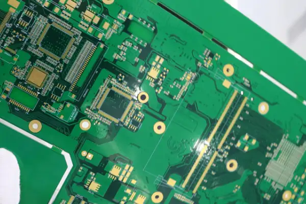
I particularly enjoy observing the differences between PCBs from different manufacturers under a microscope. Some manufacturers control the copper plating thickness with extreme precision, while others show obvious unevenness. These subtle differences may not be noticeable in low-speed circuits, but they can produce drastically different effects in high-speed signal transmission.
Recently, I encountered a very interesting case: a research and development team, when designing a communication device, focused too much on the performance indicators of individual components. As a result, after the entire board was completed, they found problems with the coordination between different modules. Later, they readjusted the routing strategy and achieved better overall performance using more common components. This made me realize that local optimization does not equal global optimization.
The longer you work in this industry, the more you realize that good design often lies in the attention to detail. For example, when a client later adjusted their design, we suggested controlling the trace lengths of certain critical signals within a specific range. This seemingly simple change significantly improved the stability of the entire system.
Now, whenever I review a new PCB design, I pay special attention to those easily overlooked fundamental aspects. After all, even the most advanced theories must ultimately be implemented through a concrete circuit board, and every detail in the manufacturing process can become a key factor affecting the final result.
Recently, in conversations with some high-speed PCB manufacturers, I found that many people oversimplify impedance control. They think that as long as the trace width is set correctly, everything will be fine, but this is far from sufficient.
I remember last year a client came to us with their design drawings. Their board needed to handle high-frequency signals, but the initial design completely ignored the impact of interlayer dielectrics. When the sample was produced and tested, the signal integrity was found to be extremely poor. We readjusted the layer stack-up, placing the critical signal layers in more suitable positions, which solved the problem.
The most easily overlooked aspect of PCB design is interlayer matching. Sometimes, you might see that the parameters of a single layer meet the requirements. However, significant differences in material properties between different layers can lead to unexpected reflections and resonances.
I’ve seen many engineers overemphasize single-ended impedance while neglecting the balance between differential pairs. In fact, the parasitic parameters of vias can have a significant impact when signals need to transition between different layers. Once, we reduced via crosstalk by more than 40% by optimizing anti-pad design.
Many high-speed circuit boards now require special materials, but their processing methods are completely different from standard FR4. For example, the adhesive flow characteristics of some high-frequency boards are very special; lamination using the old methods will definitely cause problems.
The truly professional approach is to consider manufacturing feasibility from the initial design stage, rather than waiting until the board is ruined and then reworking it. Sometimes, a seemingly minor adjustment, such as changing the copper foil roughness or adjusting the prepreg arrangement, can significantly improve overall performance.
Good design isn’t about piling on high-end parameters, but about ensuring that every element works in harmony. Like playing a symphony, every instrument must be perfectly positioned to create a harmonious melody.
I recently chatted with a friend who works in circuit design. He said that when choosing a high-speed PCB manufacturer, many people only focus on the die loss (Dk) value of the board material, which is somewhat one-sided. Material loss is often much more complex than we imagine, especially when you consider the surface roughness of the conductor.
I’ve seen many cases where engineers spend a lot of money on low-Dk materials, only to find that the conductor loss at high frequencies actually increases due to inadequate copper foil surface treatment. Think about it: when signals travel fast, the current is concentrated on the conductor surface. If the surface is bumpy, the electrons have to travel a bumpy path, and all the energy is wasted on friction and heat.
Some manufacturers like to boast about how low the dielectric loss of their materials is, but in real-world applications, the conductor and dielectric are often mutually restrictive. For example, if you use ultra-smooth copper foil but pair it with a substrate with poor thermal stability, temperature fluctuations will completely disrupt the loss characteristics of the entire system.
I remember once testing and comparing two solutions: one using ordinary copper foil with a top-tier dielectric, and the other the other way around. The result was that above 10GHz, the latter performed more stably. What does this illustrate? Single-point optimization is less effective than overall balance.
Some high-end projects are now using composite copper foil with nanoscale surface treatments. While more expensive, it simultaneously reduces conductor loss and dielectric interference. However, this process demands extremely high manufacturing precision, and not all factories can achieve stable mass production.
Ultimately, choosing materials is like choosing clothes—you can’t just look at how beautiful each piece is; you have to consider the overall harmony. After all, signal transmission is a systems engineering problem, and any bottleneck can lead to failure.
I recently chatted with a hardware design engineer and noticed an interesting phenomenon: many people think that choosing PCB materials is simply a matter of looking at the numbers on the parameter list, as if simply increasing parameters like loss factor and dielectric constant will solve the problem. But it’s not that simple, especially when you actually work with high-speed PCB manufacturers. You’ll find that material selection involves much more than just comparing technical parameters.
I remember once when our team was designing a high-frequency signal board, we initially chose a substrate with exceptionally high nominal performance. However, the signal integrity of the prototype consistently failed to meet standards. After repeated communication with the manufacturer, we discovered the problem lay in the weaving method of the fiberglass cloth—the texture of that material was too pronounced, causing inconsistent signal propagation speeds in different directions. This detail wasn’t even mentioned in the datasheet.
This made me realize that often we focus too much on the theoretical performance indicators of materials, neglecting the variables in actual manufacturing. For example, two materials with the same nominal loss factor can exhibit vastly different performance after lamination because the uniformity of the adhesive content directly affects the stability of the final product. Experienced manufacturers will tell you that while some materials perform excellently in laboratory environments, their thickness tolerance control in mass production is not as stable as that of established materials.
Now, my team and I prioritize manufacturing feasibility when selecting materials. Instead of pursuing the newest and most expensive materials, we choose mature solutions that have been validated through large-scale production. After all, even the best materials are just empty talk if they cannot be produced stably.
In a recent project, we used a relatively traditional fiberglass cloth substrate, but optimized the laminate structure, and it performed better than blindly pursuing high-end materials. This reinforced my belief that the right material is always more practical than the one with the most impressive specifications.
I’ve seen many engineers misunderstand high-speed PCB manufacturing. They often focus on material selection while neglecting more fundamental aspects. I remember a project where neglecting early testing resulted in the entire batch of boards needing rework—a lesson I learned the hard way.
Finding the right high-speed PCB manufacturer is crucial, and this isn’t just a casual remark. Good manufacturers will repeatedly confirm design details with you before production, especially those prone to problems. They won’t wait until the last minute to tell you where the problem is; they’ll be involved from the beginning to help you avoid many pitfalls.
Impedance control sounds simple, but it’s a completely different story. I once encountered a signal integrity issue that, upon closer inspection, turned out to be caused by a tiny deviation in the manufacturing process. Now, I pay particular attention to a manufacturer’s actual impedance control capabilities, not just their advertised parameters.
Testing is often underestimated, but I believe it’s where a manufacturer’s professionalism is most evident. Some manufacturers treat testing as a routine task, while truly professional manufacturers see it as the best opportunity to discover problems. They proactively record data from each test and can even help you analyze potential design risks.
PCB製造 is not simply processing supplied materials; it requires close cooperation between both parties. I increasingly believe that finding truly knowledgeable partners is more important than pursuing so-called top-tier materials, as they know how to optimize costs while ensuring performance.
Many people overemphasize layer count and advanced processes, but often problems arise in the most basic aspects. For example, improper via handling or inadequate control of trace spacing—seemingly simple things—often determine the success or failure of the entire project.
I now value a manufacturer’s actual case studies more than their equipment list. I’ve seen too many manufacturers claiming to have the most advanced equipment, yet they can’t even achieve basic process consistency. Truly reliable manufacturers will honestly tell you their strengths and limitations instead of making promises they can’t keep.
Ultimately, choosing a manufacturer is like finding a partner; you need to assess their professional attitude and problem-solving abilities, not just look at the price or the impressive figures in their promotional materials.
I’ve always found choosing a high-speed PCB manufacturer quite interesting. Some clients immediately ask about prices, but what you should really care about is whether they understand your design intent. I’ve seen a case where engineers used a high-end material for a server motherboard prototype and found severe signal attenuation. Later, after switching to another manufacturer, they discovered the problem lay in the material composition—they suggested replacing two layers with a substrate with a more stable dielectric constant, and the performance immediately met the requirements.
Many manufacturers now advertise how advanced their equipment is, but what truly differentiates them is the depth of their understanding of materials. Once, during a factory visit, I saw them conducting comparative tests using high-speed materials from different suppliers; they even clearly recorded the dielectric constant changes after temperature cycling—this kind of attention to detail reflects professionalism.
High-frequency circuits are most vulnerable to impedance abrupt changes. I remember a 5G base station project where, to save costs, ordinary FR-4 was initially chosen, resulting in significant signal distortion in the millimeter-wave band. Later, they switched to specialized high-speed materials; although the unit price increased by 20%, the yield rate improved by 30%, making it more cost-effective.
A good manufacturer should be able to help you make the choices. For example, radar boards used in autonomous driving require both low loss and heat dissipation. They might suggest using PTFE for critical signal layers and more cost-effective modified epoxy resin for other layers. This mixed-material approach saves 15% in cost compared to using only high-end materials.
Recently, I’ve noticed a trend: more and more manufacturers are offering design simulation support. One client’s self-designed high-speed traces consistently had overshoot issues. The manufacturer’s technical team directly participated in the layer stack adjustments, optimizing the reference ground plane position, and the problem was solved. This collaborative model is far more valuable than simply order-based production.
Ultimately, choosing a manufacturer is like finding a partner; size alone isn’t enough. You need to consider whether they’re willing to invest the time to understand your product’s application scenario. After all, even the best materials and technologies must ultimately serve the actual application.
I’ve seen many engineers overcomplicate high-speed PCB design. In reality, the most fundamental manufacturing process often determines success or failure. Once, our team’s design showed impressive simulation data, but actual testing consistently revealed inexplicable signal attenuation. After two weeks of troubleshooting, we discovered that the foundry had used an unsuitable etching solution ratio, causing invisible jagged edges on the critical differential pairs.
This experience made me realize that even the most precise design drawings ultimately undergo a physical transformation process like etching. When forming those micron-level circuits, if the copper foil crystallization direction isn’t taken into account, even the most expensive substrate will be wasted. A common misconception is that more layers require stacked high-pressure, high-temperature parameters; in fact, multilayer board lamination requires a rhythm as precise as kneading dough. Too much speed and force can cause uneven resin flow in the prepreg, leaving hidden stress points.
Now, when I communicate with high-speed PCB manufacturers, I pay special attention to the details of their process connections. For example, is there sufficient stress release time after lamination, or are the hole walls treated immediately after drilling? These seemingly minor aspects often reflect the true level of a factory more than the equipment model. During a recent visit to a long-established manufacturer, I discovered they even adjust the ventilation in their etching workshop according to daily temperature and humidity; this sensitivity to subtle variables is key to manufacturing high-end circuit boards.
The real test of a manufacturer’s skill isn’t the control of conventional parameters, but their ability to handle special design requirements. For example, once we needed to create a deep blind via structure within a 0.8mm thick board. Most manufacturers refused outright, but our partner achieved uniform via metallization by adjusting the pulse plating parameters. This kind of flexibility often reveals a manufacturer’s level more clearly than technical specifications.
Ultimately, good high-speed board manufacturing should be like cooking top-quality ingredients—it requires precise temperature control but also knowing when to let go. Excessive intervention can damage the material’s inherent properties; mastering this balance requires long-term experience.
I always laugh when I see PCB manufacturers claiming to handle high-speed signals boasting about their capabilities. This industry truly tests not how cutting-edge the equipment is, but how deep an engineer’s understanding of electromagnetic fields is.
I’ve seen too many designs that perform flawlessly in the lab but fail in real-world applications. A client who makes communication base stations once asked me to help identify the differences between samples from three suppliers. Superficially, the board parameters seemed similar, but in actual testing, only one supplier could maintain stable signal integrity. Later, it was discovered that the key difference lay in their methods of controlling the dielectric layer thickness. A reliable manufacturer controlled the thickness fluctuation of each dielectric layer to the micrometer level, while the other two focused solely on boasting about their imported materials, neglecting the most basic process stability.
Many manufacturers now like to confuse high-speed and high-frequency, but the technical focuses required for these two are completely different. High-speed focuses more on signal timing, while high-frequency considers electromagnetic wave propagation characteristics. For example, in a previous radar project, the PCB needed to handle 77GHz high-frequency signals while ensuring synchronization accuracy between multiple channels. The supplier they found couldn’t even do basic impedance matching properly, yet repeatedly emphasized that they purchased top-grade substrates.
Truly professional high-speed PCB manufacturers focus more on detail control. For instance, a Guangdong manufacturer we worked with had a particularly interesting step in their quality control process: using ultrasonic scanning to scan the internal structure of each multilayer board. This testing method can detect potential delamination risks earlier than conventional electrical testing. One of their engineers made a very practical point:
When choosing a manufacturer, I particularly value their willingness to share simulation data from the design process. Once, while participating in an autonomous driving project, a supplier proactively provided a 3D electromagnetic field simulation report for signal integrity, clearly marking the field strength distribution at the vias. This transparent collaboration was far more reassuring than empty promises.
In fact, there’s a simple way to judge a manufacturer’s reliability: observe how they handle unconventional customer needs. Last year, we needed to produce a batch of boards for data center switches. One manufacturer refused outright when they heard we needed to achieve a 12-layer structure within 0.8mm thickness. Another company, however, organized a dedicated team, spent three weeks readjusting the lamination process, and ultimately not only achieved it but also developed a set of production standards for thin multilayer boards.
Ultimately, what this industry lacks most isn’t high-end equipment, but rather the craftsmanship spirit of those willing to dedicate themselves to solving real-world problems. Good high-speed PCB manufacturers should be like experienced traditional Chinese medicine practitioners, accurately diagnosing problems and flexibly adapting solutions. Factories that only operate according to standard procedures will never achieve true technological breakthroughs.
In the field of industrial automation, people often pay attention to AI
Ever wonder how your phone maintains a stable signal? It relies on
When selecting components for a security monitoring system, most attention goes to
- 小・中ロット生産のエキスパート
- 高精度PCB製造と自動アセンブリ
- OEM/ODM電子プロジェクトの信頼できるパートナー
営業時間:(月~土)9:00~18:30