
From Novice to Expert: Sharing My Experience in Pin Header PCB Selection
As an electronics enthusiast, I’ve come to understand firsthand the impact of
Every time I see those densely packed BGA packaged chips lying on the circuit board, I always think about how many details need to be carefully considered, especially when you are considering choosing a PCB Fabrication supplier. When working with Chinese suppliers, you realize that not all manufacturers can handle those minute details well.
I remember once designing a project that required 0.4mm pitch BGAs. Some members of the team thought that as long as the drawings were done and handed over to the factory, everything would be fine. However, when the first batch of boards arrived, numerous problems arose during soldering. We later discovered that the issue stemmed from inconsistent pad sizes; some pads were too large, others too small, leading to unstable connections after soldering. Since then, I’ve paid particular attention to suppliers’ ability to handle details, especially seemingly insignificant parameters like the width of the solder mask bridge. Although small, it plays a crucial role in preventing short circuits.
Speaking of BGAs, many people immediately think of high density and high performance. But I believe the real test of a manufacturer’s skill lies in how they handle these intricate structures, rather than simply pursuing higher layer counts or wider trace widths. I once worked with a domestic manufacturer who demonstrated solid performance in handling fine-pitch BGAs without blindly promoting themselves. Instead of focusing on achieving the highest possible specifications, this pragmatic approach of ensuring the flatness of each solder pad gives me more peace of mind. I know that in practical applications, reliability is often more important than theoretical parameters.
Another aspect that impressed me was the choice of surface treatment. Some people tend to pursue the latest processes, but I’ve found that traditional ENIG treatments are sometimes more reliable in terms of long-term stability. Of course, this requires strict quality control from the manufacturer; otherwise, black pad issues could become a hidden danger. I’ve seen cases where choosing an unsuitable surface treatment in pursuit of low costs led to product failures after only a few months. This reminds us that when selecting suppliers, we shouldn’t only look at the price but also at their ability to guarantee quality at every stage.
In general, I think that when dealing with high-density components like BGAs, we need to focus more on the manufacturer’s practical experience and attention to detail, rather than being misled by impressive specifications. After all, good design requires solid manufacturing support.
I’ve noticed a particularly interesting phenomenon after working in the PCB Fabrication China field for a while—many purchasing personnel focus too much on price comparisons and neglect more crucial factors. Last year, we had a project that required a new supplier to manufacture a batch of high-frequency boards. We inquired with seven or eight factories, and the lowest quoter couldn’t even provide a basic impedance test report, while another, slightly more expensive supplier could provide complete material traceability records.
Choosing a PCB supplier is a bit like finding a fitness coach—it’s not about who charges the lowest price, but who truly understands your needs. Once, we had a project where we urgently needed prototyping, and the other party’s engineer was still discussing layer stack-up design with us late at night. This level of cooperation is far more valuable than simply having a price advantage.
Many companies are now focusing on the green transformation of their supply chains, but I think we can’t just look at the surface. Last month, I visited a factory that claimed to have a carbon accounting system, only to find that their energy consumption monitoring was still at the manual meter reading stage. True digital management should be like the Dongguan factory we cooperate with, where every machine can provide real-time energy consumption data.
The small-batch trial production stage is actually the stage where problems are most likely to be exposed. I usually require suppliers to provide detailed process parameter records at this stage. One manufacturer in Shenzhen did this very well; they even sent us the etching solution concentration change curves for each batch. This transparency is reassuring.
Many people think that bulk purchasing is all about price reduction, but I’ve found that the truly smart approach is to build long-term relationships with high-quality suppliers. We have a manufacturer we’ve been working with for three years; now they not only prioritize our schedules, but their engineers also proactively suggest new processes to reduce costs. This kind of tacit understanding takes time to build.
Ultimately, PCB procurement isn’t a simple buyer-seller relationship, but a process of technical collaboration. Good suppliers can become your external support team; those who only focus on price often end up hindering things.
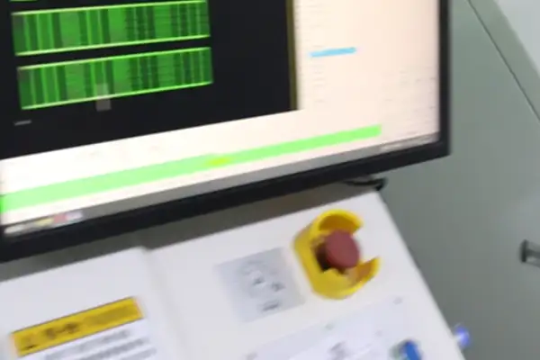
In my years of PCB procurement in China, I’ve noticed a rather interesting phenomenon: many people instinctively associate domestic manufacturing with low prices. But the situation has changed drastically. I remember last year, when helping a client find Ultra HDI suppliers, I visited several factories in the Pearl River Delta. One company’s workshop had a laser drilling machine customized from Germany, and the industrial control screen displayed real-time alignment data down to the micrometer level. The engineer pointed to the purplish-glowing boards in front of the glass window and said that even the breathing frequency of these high-density boards needs to be controlled, because even a 0.1% fluctuation in humidity can cause invisible cracks in the dielectric layer. The workshop’s temperature and humidity control system can even be zoned to ensure consistent material properties across each process stage. This environmental control capability is comparable to that of Japanese and Korean counterparts.
However, the real test of technology comes from seemingly ordinary routine orders. Once, during a batch production of six-layer boards, a customer requested a last-minute change to the linewidth from the standard 6mil to 4mil. Two of the three alternative manufacturers produced samples with jagged edges, while only one manufacturer using a pre-expansion/expansion process achieved perfectly straight lines. This experience made me realize that high-end manufacturing doesn’t necessarily require pursuing extreme parameters; a thorough understanding of fundamental processes is the true skill. The successful factory had actually performed a 24-hour environmental adaptability treatment on the substrate before lamination, eliminating the impact of internal stress on fine lines.
Now, many European and American customers, when approaching Chinese suppliers, always emphasize needing “top-tier technology,” but often overlook the issue of compatibility. For example, a customer manufacturing medical imaging equipment insisted on using mSAP technology, even though their board’s signal rate was less than 10Gbps. Later, we suggested switching to a modified negative film process with low-roughness copper foil. This reduced costs by 30% and also passed more stringent temperature cycling tests. Sometimes, excessively chasing technical labels can lead to a loss of direction. For example, while mSAP offers high precision, its corresponding DFM rules limit design flexibility. The modified negative film process, however, can better balance performance and cost in boards with 8 layers or less.
I recently gained a deeper understanding while working on an automotive radar project. The client initially specified a Japanese M7 grade material, but a domestic manufacturer achieved similar dielectric constant stability using a proprietary hydrocarbon resin formula. Crucially, their lamination process precisely controlled the Z-axis expansion coefficient—a critical factor for phase consistency in high-frequency boards. Looking at their modified vacuum laminator in their lab, I suddenly realized that Chinese PCB fabrication is forging its own technological path. They even developed a special filler dispersion technology, ensuring that the Dk value of the resin system fluctuates by less than 2% within the -40℃ to 150℃ range.
Actually, there’s a very intuitive way to judge a supplier’s level: observe how they handle abnormal data during production. During a visit, an unexpected incident occurred: the copper thickness of the micropores in a batch of HDI boards exceeded the standard by 0.3 micrometers. This was perfectly within the customer’s tolerance range, but their quality engineers insisted on tracing it back to fluctuations in nitrogen purity during the annealing process. This obsession with detail is more convincing than any certification. It was later discovered that the molecular sieve in the nitrogen generator had a 0.3% performance degradation; this level of control extends to the second level of the supply chain.
Of course, some situations are also quite frustrating. Some suppliers, clearly manufacturing consumer electronics boards, insist on claiming to produce military-grade products, but when asked about the details of the descaling process after drilling PTFE materials, they become evasive. Conversely, one manufacturer specializing in industrial control had a technical director who could readily draw the impedance impact curves of eight different fiberglass cloth weaving methods on a whiteboard—this kind of solid knowledge cannot be faked. For example, the difference in dielectric layer thickness between 106 and 1080 weaves can cause a characteristic impedance fluctuation of up to 3 ohms; this kind of microscopic knowledge requires years of practical experience.
Ultimately, choosing a supplier is like finding a partner; simply looking at hardware specifications is far from enough. A Shenzhen company I worked with last time left a deep impression on me: they built dedicated process databases for each key client, and even the operators on the immersion gold line could describe the deposition rate curves of a certain German brand of chemicals at different pH values. This approach of embedding technology into the very core of the process may be the true upgrade happening in Chinese manufacturing. Their database even included the impact of tap water ion concentration on cleaning effectiveness in different seasons; this level of data granularity improved process stability by 15%.
I’ve been working in the PCB industry for over a decade. Many people think that finding a cheap PCB fabrication manufacturer in China will solve everything. However, problems often arise in the design phase. Once, our team designed a board with BGA packaging. To meet deadlines, we skipped several simulation steps. The result was a shockingly low BGA soldering yield on the sample. We had to rework it three times to barely meet the requirements.
That experience taught me a valuable lesson: a truly reliable manufacturer isn’t the one with the lowest price, but rather a partner who can work with you to scrutinize the design details. A client who manufactures medical equipment left a lasting impression on me. They brought the PCB supplier into the review process during the design phase. Engineers from both sides meticulously compared the thermal parameters of each BGA. The final mass production yielded almost zero defects.
Now, I get a headache seeing procurement methods that only compare prices. Good PCB manufacturing should be like a skilled traditional Chinese medicine doctor treating an illness. It needs to start from the design stage. Especially now that chip pins are getting increasingly dense, the traces under the BGAs are practically a maze. Just the other day, a customer complained that a certain manufacturer couldn’t solder 0.35mm pitch BGAs properly. I checked and found they hadn’t implemented thermal deformation compensation at all.
Actually, some PCB manufacturers in China are quite impressive. They proactively offer improvement suggestions during the engineering confirmation phase. For example, changing vias around critical BGAs to blind vias, or adjusting the solder mask window size. This collaborative model is far better than post-production wrangling. After all, the biggest loss from a bad board is project schedule.
I often tell my team not to treat the PCB as an ordinary component. It’s more like the skeleton of the product. If the skeleton is crooked, even the best chips are useless, especially on high-density boards using multiple BGAs. Material compatibility should be considered from the design stage. Sometimes, changing the substrate can prevent overall board warping.
Recently, an interesting phenomenon has emerged: some clients are starting to request design specification documents from PCB manufacturers. This indicates that everyone is finally realizing that manufacturing capabilities should be prioritized in the R&D phase. After all, nobody wants to discover an unreasonable BGA pad design only during surface mount technology (SMT).
While reviewing project data from the past few years, I recently discovered an interesting phenomenon: our team’s choice of PCB suppliers at different stages shows a clear pattern. Early projects mostly focused on finding manufacturers in the Pearl River Delta region; later, as product complexity increased, we shifted to the Yangtze River Delta; and recently, two industrial-grade projects opted for suppliers in the central and western regions.
This shift in choices reflects a reassessment of the manufacturing capabilities of different regions. Many people automatically associate PCB Fabrication China with Shenzhen’s fast-turn board factories; however, the manufacturing characteristics of different regions in China are far more diverse than imagined. During a visit to Suzhou, we were impressed by the local factory’s processing technology for military-grade boards; while a flexible board production line at a company in Chengdu completely overturned my perception of the manufacturing level in inland China.
I remember a medical equipment project that caused us considerable trouble. To meet deadlines, we initially chose a Shenzhen manufacturer that claimed to produce samples within 24 hours. However, during mass production, we discovered that impedance control consistently failed to meet requirements. We later realized that such precision boards require sophisticated manufacturing processes, not just speed. This experience taught me that supplier selection cannot be based solely on superficial promises; it’s crucial to thoroughly examine whether their technological expertise matches the product’s characteristics.
Now, we proactively adjust our procurement strategies based on product type. Consumer electronics are indeed well-suited to the Pearl River Delta’s rapid response system; however, for automotive electronics or industrial control, we prefer specialized factories in the Yangtze River Delta or inland regions. These companies may not constantly tout “fastest prototyping,” but they often possess unique strengths in material selection and process control.
Recently, during a conversation with German colleagues, they raised an interesting point: the biggest advantage of China’s PCB industry isn’t the prominence of any particular region, but rather the formation of a complementary manufacturing ecosystem. I deeply resonate with this view; for example, in our smart home project last year, the motherboard was manufactured in Dongguan, the sensor boards in Suzhou, and final assembly in Chongqing—each step utilized the most mature local manufacturing resources.
This regional specialization is changing traditional procurement logic. In the past, we always sought “all-rounder” suppliers; now, we focus more on building a modular supply network. After all, different regions have different manufacturing philosophies; rather than forcing a single factory to master all processes, it’s better to activate the most suitable manufacturing capabilities based on product needs.
In my years of experience in PCB manufacturing in China, I’ve noticed an interesting phenomenon: many people associate domestic PCB manufacturing with low-price competition. In reality, the technological stratification within the industry is more pronounced than imagined.
I remember last year a client came to me with a price list from overseas for comparison. He originally thought domestic manufacturers could only produce basic double-sided boards. He was surprised when we showed him a sample of a 20-layer board. This kind of misconception is quite common.
The development speed of HDI technology has exceeded many people’s expectations. Technologies that were considered high-end five years ago are now standard in mid-range products. Once, I visited a factory in Suzhou and saw them using laser drilling technology to process 0.1mm micro-holes—the entire process was fully automated. In the past, this level of precision processing might have required sending it overseas. Especially in the fields of medical devices and high-frequency communications, the requirements for micro-aperture precision are even more stringent. Domestic manufacturers have already achieved aperture tolerance control within ±10μm, which directly determines the stability of signal transmission and the reliability of equipment.
The industrial agglomeration effect in the Yangtze River Delta region is indeed significant. However, I’ve noticed a phenomenon: many small and medium-sized manufacturers have their own expertise in specific areas. For example, a company in Dongguan specializes in flexible circuit boards; their products used in wearable devices have precision that is in no way inferior to those of large manufacturers. These companies typically employ a deep customization strategy, such as developing irregularly shaped circuit boards for smartwatch manufacturers or designing special substrates that can withstand tens of thousands of bends for medical monitoring equipment. This flexibility is difficult for large standardized factories to match.
The pace of technological iteration is accelerating. Standard processes that were mainstream three years ago may now be outdated. This necessitates continuous investment in research and development by manufacturers. Some manufacturers I know allocate over 15% of their annual profits to new equipment purchases and technology upgrades. For example, the mSAP process, widely adopted this year, enables 8μm linewidth and spacing on 5G antenna boards, whereas the industry standard was 12μm just six months ago. This rapid iteration allows for a roughly 40% increase in the design density of mobile phone motherboards every two years.
The differences in quality control systems are often underestimated. For example, when producing eight-layer boards, some manufacturers can achieve a 99% yield rate, while others may still be hovering around 90%. This gap cannot be solved simply by changing equipment; it involves optimizing the entire production process. Excellent factories establish a full-process data traceability system, monitoring over 200 parameters in real time at each stage, from substrate warehousing to finished product shipment. One company in Zhuhai has even developed an AI visual inspection system capable of identifying micron-level copper foil defects that are difficult for humans to detect.
Recently, a trend has been observed: more and more customers are focusing on environmentally friendly processes. This is forcing manufacturers to improve their production processes. One company in Shenzhen has not only reduced pollution but also saved 30% on water and electricity costs through a wastewater recycling system. Their cyanide-free gold plating process halved wastewater treatment costs while simultaneously improving gold layer uniformity to ±0.05μm. This win-win case of environmental protection and quality is spreading throughout the industry.
Supply chain stability is often overlooked. During the pandemic, one factory was able to deliver on time because it had stockpiled raw materials in advance. This foresight, which may not be apparent under normal circumstances, becomes a core competitive advantage in critical moments. For example, some manufacturers establish joint inventory mechanisms with copper foil suppliers or invest in copper-clad laminate modification technologies to adapt to various material alternatives. This supply chain resilience can maintain a 5%-8% cost advantage when raw material prices fluctuate.
I believe that in the next few years, the domestic PCB industry will see more specialized companies in niche areas. They may not be large in scale, but they will have strong competitiveness in specific technical fields. This specialization is very helpful in improving the overall level of the industry. For example, some companies specialize in high-frequency material applications for automotive radar boards, while others focus on heat dissipation solutions for Mini-LED backlight boards. This deep specialization allows them to achieve gross profit margins of over 35% in their niche markets.
Every time I see domestically produced circuit boards used in high-end equipment, I feel that this industry still has great potential. After all, progress in manufacturing is achieved through real, tangible efforts, not just marketing hype. A recent teardown of a flagship smartphone revealed that six key modules on its motherboard used HDI boards from domestic manufacturers. This demonstrates that domestic technology has gained recognition from leading clients in terms of signal integrity and heat dissipation performance.
I have some experience in finding PCB suppliers. Many people immediately focus on price, thinking the cheaper the better, which is a misconception. I’ve seen too many cases where seemingly attractive low prices hide unexpected additional costs. For example, some suppliers charge separate engineering fees or set very high minimum order quantities, resulting in increased inventory pressure. Worse still, they might secretly use lower-specification materials to cut costs.
I especially want to warn everyone to be wary of suppliers who claim to be able to do everything. While the PCB Fabrication China sector is indeed developing rapidly, each factory has its strengths and weaknesses. Some factories advertise the ability to produce any layer of HDI boards or ultra-high multilayer boards, but their actual mass production yields are alarmingly low. In such situations, it’s best to request production records for similar products from the other party, and if possible, visit their factory in person to assess their manufacturing processes.
Language communication is also an easily overlooked issue. We once worked with a factory that had good technical capabilities, but due to time zone differences and language barriers, emails were often replied to only the next day, and problems encountered during production couldn’t be resolved promptly. Later, we switched to a supplier with a professional foreign trade team, and efficiency improved significantly. Now, I pay special attention to the supplier’s response speed and service awareness, which avoids many subsequent problems.
Ultimately, choosing the right supplier shouldn’t be based solely on the cost of a single transaction. As industry environmental requirements become increasingly stringent, supply chain stability becomes even more crucial. Manufacturers who can find a balance between rapid prototyping, stable production, and environmental compliance are worthy of long-term cooperation. Establishing a comprehensive evaluation standard, including technical strength, quality system, and sustainable development capabilities, ensures that the selected partners truly contribute to your business development rather than hinder it.
Recently, helping a friend with PCB prototyping reminded me of some characteristics of domestic PCB manufacturing. Many people’s understanding of domestic manufacturing processes is still stuck in the past, believing they can only produce basic boards. This view needs to be updated. I’ve contacted several PCB fabrication manufacturers in China, and their breakthroughs in specialized processes are truly surprising.
Take microvias, for example; the precision they can achieve now is quite impressive. I once saw a microvia cross-section they drilled with a laser, and the smoothness of the hole walls was much better than I had imagined. Five years ago, this kind of precision work might have relied on imported equipment, but now domestically produced equipment can reliably output this level of precision.
Regarding surface treatment, I’ve noticed many people blindly pursue high-cost solutions. In fact, basic treatments like OSP (Surface Mount Technology) are more practical in the right context. I worked on a smart home project that insisted on using an OSP solution, and the product performed better than expected in a humid environment. The key is to control the quality of incoming materials. If the substrate itself meets the standards, the soldering effect of OSP is not inferior.
However, it’s important to pay attention to the compatibility of different processes. Once, during testing, we found that the immersion silver layer on a batch of boards discolored in a high-temperature, high-humidity environment; we later realized it was due to inadequate anti-oxidation measures. These kinds of detail issues often only become apparent in actual application.
Now, I prefer to give samples to manufacturers that can provide complete process data. For example, during the impedance testing, the manufacturer directly provided records of the process parameters for each step, which was reassuring due to its transparency. After all, good manufacturing capabilities depend not only on equipment precision but also on the rigor of process control.
Sometimes, process selection cannot be based solely on parameters; it must be considered in the specific application scenario. For instance, in one industrial control project we worked on, although we used the most basic tin plating process, it proved more stable than pursuing a more advanced process because it was matched to the actual usage environment.
Ultimately, improvements in manufacturing capabilities must be reflected in practical applications. Recently, I’ve noticed some manufacturers starting to offer small-batch rapid prototyping services along with detailed process inspection reports, which is quite interesting. After all, even the most advanced processes are only valuable if they serve the actual product.
Every time I work on a new PCB project, I notice some interesting changes in details. For example, even double-sided boards can now have through-hole designs, a feature previously exclusive to high-end boards. The pace of manufacturing technology adoption is indeed much faster than expected.
In my years of experience in PCB manufacturing in China, I’ve observed an interesting phenomenon—many people are overly focused on high-end testing equipment and technical parameters. I remember once a customer came to me with an X-ray inspection report complaining about BGA soldering problems. Upon closer inspection, it turned out the board had been bent during transport, causing poor solder ball contact.
In fact, the quality of BGA soldering often depends on the most basic aspects, such as plating uniformity, which is easily overlooked. I’ve seen many factories cut corners to save costs and shorten plating time, resulting in uneven copper thickness on the hole walls. Later, heat conduction problems during soldering caused the rate of cold solder joints to double.
Through-pad designs are becoming increasingly common, but few manufacturers can truly achieve perfect fill flatness. Once, we tried using imported plating solution for copper filling, and the effect was indeed good, but the cost was 40% higher than the ordinary process. In the end, the customer chose resin plugging, since most consumer electronics products don’t require such extreme performance.
Interestingly, sometimes the simplest methods are the most effective. When processing a batch of high-density boards, we found that using a regular microscope to inspect cross-sectioned samples was more effective than fully automated inspection equipment in detecting problems promptly, especially tiny cracks that might appear as normal shadows to the equipment but are clearly visible to the human eye.
Many engineers tend to overcomplicate problems. However, the core of soldering quality lies in the stability of the basic process. I’ve seen too many cases showing that instead of pursuing expensive testing solutions, it’s more important to accurately adjust plating parameters and control solder ball size. These seemingly ordinary details are the key to determining yield.
Over the years, in electronic design, the most troublesome issue for me has been the layout of high-density chips. I remember the first time I encountered BGA packaging, I stared at the circuit board for a long time—the dense solder joints spread out like a starry sky, making it impossible to find a starting point.
Later, I realized I was overcomplicating the problem. The biggest advantage of BGA is that it simplifies routing. Although it looks dense, the actual routing can bypass the pads and pass through the middle layer. Once, I designed an industrial control board using 0.8mm pitch BGA chips, and all the routing was handled on a six-layer board. With older QFP packages, at least eight layers would have been needed.
Speaking of PCB Fabrication China, I think domestic manufacturers do have unique advantages in handling BGA. Last year, a project required BGA soldering on an aluminum substrate. Several companies said they couldn’t do it, but a small factory in Guangdong took on the order. They adjusted the reflow soldering temperature profile and succeeded on the first try.
Actually, the biggest problem with BGA isn’t soldering itself, but thermal stress. Once, during testing, we found that the chip would occasionally malfunction. After much troubleshooting, we discovered it was due to board deformation causing the solder joints to crack. We added support pillars at the four corners, and the problem was solved. These kinds of details are rarely mentioned in textbooks; they’re lessons learned through real-world projects.
Now, when I see young people designing circuits, always thinking about using the thinnest traces and the smallest vias, I want to remind them: reliability is far more important than density. Especially with industrial-grade products experiencing high temperature differences and strong vibrations, fancy designs are more prone to problems. Sometimes, using the older 0805 package is more reliable than the latest miniature BGA.
Recently, I’ve been working on an automotive project that uses BGA chips again. This time, I deliberately made the solder pads 5% larger than the standard size. Although it doesn’t look as refined, all solder joints remained intact after three high and low temperature cycle tests. This reinforces my belief that pragmatism is always more important than pursuing perfection in electronic design.
Ultimately, no matter how advanced the packaging technology, it must serve practical needs. Instead of obsessing over the latest processes, it’s better to solidify the fundamentals, since even the most sophisticated chip ultimately needs to be placed on a physical PCB to function.
I’ve always felt that many people overcomplicate PCB manufacturing, especially when it comes to BGA packaging. Last year, our team worked on a project using high-density BGA chips, and we encountered quite a few pitfalls.
I remember one board that passed all routine tests, but kept experiencing inexplicable signal loss during actual operation. After much troubleshooting, we discovered that several hidden test points were poorly designed, causing some signal paths to be unmonitored. This experience made me realize that in the field of PCB Fabrication China, the real test of skill is often not the routine processes, but these details.
The biggest challenge with BGA devices is that you can’t see the solder joints. Once, we encountered a case where the board worked normally at room temperature, but experienced connection failures at low temperatures. X-ray inspection later revealed microscopic cracks inside the solder balls. These kinds of problems are difficult to detect in routine testing, but they have a huge impact on product reliability.
I now pay special attention to the layout design of test points. Many people arrange test point positions haphazardly to save space, but this often causes significant trouble for later debugging. A reasonable distribution of test points not only improves testing efficiency but also allows for quick location of faults when problems occur.
Recently, some domestic PCB manufacturers I’ve contacted have become increasingly professional in this area. They’ve begun to adopt more refined microvia technology and layered testing schemes, which is very helpful for the quality control of BGA devices. After all, electronic devices are becoming increasingly compact, and the requirements for reliability are also increasing.
I think making a good PCB is like completing a precision instrument; every step must be taken seriously. From material selection to process control to final testing and verification, none of these steps can be omitted. Especially when the product is to be used in complex environments, these details often determine the final user experience.
Sometimes I feel it’s a pity to see some teams neglecting these fundamental tasks in order to meet deadlines. After all, even the best design can be wasted if there are problems in the manufacturing process.
I get a headache every time I see those densely packed circuit board parameter tables. To be honest, the PCB Fabrication China field is incredibly complex; it’s not something you can simply judge by price.
I’ve seen far too many people fall victim to so-called low-price suppliers. Just last week, a friend complained that a manufacturer offered an exceptionally cheap quote, but the boards they produced couldn’t even pass basic continuity tests. Such cases are commonplace in the industry.
Truly reliable suppliers will proactively discuss the details of their production processes, such as how they control impedance accuracy and what equipment they use for flying probe testing. They might even show you their recent quality inspection reports—those data are the real proof of their capabilities.
Regarding certifications, many people think ISO 9001 is sufficient, but in demanding projects, it’s not even entry-level. I particularly value whether a supplier has experience with medical or automotive electronics orders; these orders require a completely different level of rigor in their processes.
One detail that many might overlook is whether the supplier is willing to accept rush orders. Last year, we had a project where a design change was urgently needed, and our partner adjusted the production line the very next day. This flexibility is supported by a mature management system.
More and more customers are paying attention to environmental standards, which presents new challenges for PCB Fabrication China. Several companies we’ve recently partnered with are upgrading their processes to use halogen-free materials. This does require significant investment, but it’s an inevitable trend in the long run.
Actually, a very intuitive way to judge a supplier’s level is to look at their engineering team. Good manufacturers will have dedicated technical personnel to discuss design details with you, rather than just saying “this can be done, that can’t be done.”
Recently, I’ve noticed an interesting phenomenon: for some small-batch orders, it’s more suitable to find medium-sized suppliers. They are often more willing to cooperate with customers to make personalized adjustments, unlike large manufacturers who are inflexible.
Ultimately, choosing a partner is like finding a spouse; judging by appearances alone is useless. You need to understand their working methods and values. After all, the quality of the circuit board directly affects the fate of the entire product, and no one wants things to go wrong at this stage.
I encountered a rather interesting situation while processing a high-end graphics card. The board was assembled using complex BGA-packaged chips, but the customer reported that the screen would become distorted after running for a period of time. Upon disassembly, several solder joints under the largest BGA chip were blackened, clearly indicating overheating due to poor contact.
This situation reminds me of many cases I’ve encountered before. Some factories, in order to control costs, simplify certain processes in PCB fabrication, such as reducing the thickness of the immersion gold plating or shortening the anti-oxidation treatment time. Although everything tests fine when the chips leave the factory, in actual use, due to the continuous effects of thermal expansion and contraction, these cost-cutting measures easily cause problems.
This is especially true for densely pinned BGA chips, which require exceptionally high soldering quality. The most extreme example I’ve seen is a BGA on an industrial control board where improperly controlled soldering temperature led to micro-cracks at internal connection points. Initially, the equipment functioned normally, but over time, the cracks widened, eventually causing the entire system to malfunction.
Actually, there’s a very intuitive way to judge BGA soldering quality: blow hot air onto the chip for a while, then immediately test its functionality. If the temperature change causes performance fluctuations, it’s likely due to a problem with the soldering. While this method isn’t precise, it’s very helpful for quickly troubleshooting.
Many electronic products now strive for thinner and lighter designs, resulting in increasingly smaller BGA pitches, which places higher demands on PCB materials and manufacturing processes. I’ve noticed some manufacturers are starting to use new substrate materials to improve heat dissipation, which does alleviate connection failures caused by temperature changes to some extent.
However, ultimately, even the best materials require strict process control to maintain quality. Sometimes, I see repair cases where seemingly simple soldering problems escalate into major repairs requiring the replacement of the entire chip due to improper operation. This reminds us that every step in handling precision components requires extreme care.
I recently chatted with some hardware colleagues and noticed an interesting phenomenon: the factors people consider when choosing PCB suppliers are completely different now than they were three years ago. Previously, price comparison accounted for over 70% of the decision-making process; now it’s probably less than half. The experience of supply chain disruptions during the pandemic was so profound that it has fundamentally changed our perspective on the supply chain.
I just finished a smart home project last month, and a small incident in particular illustrates this point. The high-frequency board we had ordered suddenly became unavailable due to international logistics delays. My first reaction wasn’t to switch suppliers, but to ask our partner PCB Fabrication China manufacturer if they had a backup plan. Within two hours, they provided three alternative materials along with impedance test comparison data. This rapid response stems from their multi-source procurement network, where they maintain stockpiles of raw materials of different grades. This capability isn’t apparent on a price quote, but it can save a project in a critical moment.
Now, when evaluating suppliers, I pay special attention to whether they proactively share the transparency of their production milestones. For example, one supplier I frequently work with automatically pushes progress updates after each order, with time stamps for each step from board procurement to the immersion gold process. Once, their electroplating line experienced a sudden malfunction, and I immediately received a delay warning and a revised delivery schedule on my phone. While suppliers with high levels of digitalization might charge around 5% more per unit, the saved communication costs and risk premiums make it more worthwhile.
Another easily overlooked point is environmental compliance. Last year, a customer on an export order to Europe suddenly requested a carbon footprint report. Of the several factories we were working with, only the one that had proactively implemented ESG measures could immediately provide complete data because they had already integrated their energy consumption monitoring system into their production line. This incident made me realize that choosing suppliers now requires thinking three steps ahead; future trade barriers may be hidden in these details.
In fact, good PCB suppliers are no longer simply processors but partners in the product chain. Their ability to withstand unexpected risks, their willingness to invest in digitalization, and their forward-looking compliance awareness—these soft power qualities have become our most valued indicators. Price is certainly important, but when the entire industry is focused on cost control, partners who can enhance supply chain resilience are truly rare.
As an electronics enthusiast, I’ve come to understand firsthand the impact of
Why is green the universal choice for circuit boards? Behind this seemingly
As a hardware entrepreneur, I often see teams fall into a trap
- Expert en production de petites et moyennes séries
- Fabrication de circuits imprimés de haute précision et assemblage automatisé
- Partenaire fiable pour les projets électroniques OEM/ODM
Heures d'ouverture : (Lun-Sam) De 9:00 à 18:30