
Why does your Motor Drive PCB always “retire” early?
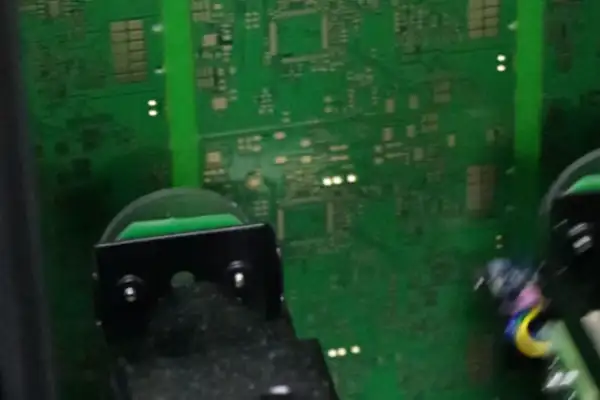
The motor drive circuit board in industrial equipment failed after long-term operation,
I recently noticed an interesting phenomenon while chatting with some friends who work in communication equipment: when discussing high-frequency PCBs, everyone tends to focus on the fancy parameter specifications. However, what truly determines the quality of a board is the most basic material selection—for example, the type of resin you use directly affects signal transmission quality.
Last year, I recall a project where the wrong resin was used, causing severe signal attenuation across the entire batch of boards at high frequencies. Switching to a specially formulated modified polyphenylene ether resin resolved the issue. This experience made me realize that high-frequency performance isn’t simply achieved by piling on high-end materials.
Many people believe that using the latest high-frequency PCB network is all they need. However, the reality is that different applications have vastly different requirements for dielectric loss—base station equipment and medical imaging equipment have completely different levels of sensitivity to dielectric constant.
The most egregious example I’ve seen is a manufacturer blindly pursuing low dielectric constants, resulting in insufficient mechanical strength of the boards and delamination under temperature changes. These problems often only surface during mass production, causing significant losses.
Some manufacturers now like to tout new materials like quartz cloth as miraculous, but in ordinary applications, second-generation fiberglass cloth is perfectly adequate. The key is proper impedance matching design. Like building blocks, not all components need to be made with the most expensive materials; a well-designed structure is often more important than improving the performance of a single material.
I recently tested several domestically produced resin materials and found that their performance in specific frequency bands is comparable to imported products, especially in terms of thermal stability in specific application scenarios. This might mean we don’t need to always focus on foreign brands.
Ultimately, designing high-frequency circuit boards is like cooking with high-end ingredients—it’s not about piling on expensive ingredients to create a delicious dish. The real challenge lies in finding the most balanced recipe based on specific needs. This process often requires repeated adjustments to achieve the ideal effect.
While researching high-frequency circuit board design recently, I discovered an interesting phenomenon: many people overemphasize the dielectric constant of materials while neglecting the importance of overall system synergy. I remember once testing a high-frequency PCB in the lab. Despite using a substrate with a nominally ultra-low dielectric constant (DK), the actual signal integrity was not as expected. It was later discovered that the surface treatment of the copper foil affected high-frequency performance, causing unnecessary scattering of electromagnetic waves on the conductor surface.
This reminds me of the industry’s blind pursuit of Low-DK materials. While reducing the dielectric constant does reduce signal delay, the truly crucial factors determining the stability of high-frequency circuits are often those easily overlooked details. For example, the microscopic roughness of copper foil directly affects the skin effect, and the matching degree of thermal expansion coefficients between the substrate and the conductor is crucial for long-term reliability. I’ve seen too many cases where excessive pursuit of a single parameter has actually compromised the performance of the entire high-frequency PCB network.
An engineer working on radar systems shared his experience with me. They had tried various high-end Low-DK materials. Ultimately, they found that the most suitable solution was a traditional material with a moderate dielectric constant but excellent stability, because their equipment needed to operate in environments with a 40-degree temperature difference. Some new materials claiming ultra-low DK exhibited significant parameter drift at high temperatures. This reminds us that we need a systemic approach to material parameters.
Many manufacturers now like to advertise the extreme performance parameters of materials, but rarely mention their performance in actual working environments. Just like when choosing copper foil, you can’t just look at the initial roughness data; you also need to consider the surface morphology changes after multiple hot pressings. Some HVLP copper foils have excellent parameters when they first leave the factory, but are prone to changes in crystal orientation during multilayer lamination.
I think high-frequency circuit design is more like solving an equation that requires balancing multiple factors. Simply pursuing low values for a single parameter can be misleading. After all, the electromagnetic environment in real-world applications is far more complex than in a laboratory setting. The interactions between materials are often more important than the performance of individual materials. This is why some seemingly ordinary material combinations can exhibit more stable high-frequency characteristics.
A recent experience debugging a millimeter-wave circuit for a friend exemplifies this point. We experimented with three different DK-grade substrates paired with RTF copper foil and found that a material with a medium DK value but a more stable loss tangent reduced the bit error rate by 15%. This demonstrates that when selecting materials for high-frequency circuits, we need to move beyond a parameter-race mentality and consider the needs of the actual application scenario.
Perhaps we should re-examine the definition of “high performance.” In the high-frequency field, sometimes moderate compromises can yield better overall performance. This requires designers to have a more comprehensive understanding of the characteristics of different materials, rather than just focusing on a few prominent parameters in the datasheet.
I recently chatted with some friends who work in hardware procurement and discovered an interesting phenomenon. They are always struggling with which high-frequency PCB supplier to choose. Actually, it’s not that complicated. The key is to understand what level of performance your product actually requires. For example, making base station antenna boards and making high-frequency boards for automotive radar are completely different things. Some manufacturers’ exaggerated specifications may be completely useless in real-world scenarios.
I remember last year we almost got misled by a supplier on a project. They kept emphasizing how advanced their Low-DK material was. But actual testing revealed that while the dielectric constant was indeed low, the loss factor was ridiculously high. Later, switching to a manufacturer specializing in specialty resin systems solved the problem. So now I think suppliers are more important than their technological accumulation, rather than the impressive numbers in their brochures.
The changes brought about by 5G deployment are more profound than imagined. Previously, it might have seemed like simply upgrading equipment in a traditional PCB factory was enough to make high-frequency boards. Now, that idea is incredibly naive. Last week, I visited a lab and saw their testing scenarios simulating the 6G band. Even micron-level roughness of the copper foil can affect signal integrity. This level of precision is beyond the capabilities of ordinary factories. Especially in the millimeter-wave band, electromagnetic waves exhibit the skin effect, and even tiny imperfections on the conductor surface can exacerbate signal attenuation.
I’ve noticed that excellent purchasing managers all do one thing: translate technical specifications into production language. For example, impedance control isn’t simply about looking at tolerance ranges. They need to clarify the manufacturer’s compensation scheme and how linewidth error is controlled. These details often reveal more than certification certificates. For instance, some manufacturers use direct laser imaging technology to ensure linewidth accuracy, which is more precise than traditional exposure processes, controlling errors within ±0.02mm.
Several emerging application scenarios I’ve recently encountered are quite interesting. Satellite internet terminals require high-frequency boards that are both lightweight and resistant to extreme environments. This is forcing material manufacturers to develop more flexible composite substrates, which in turn brings new ideas to traditional communication equipment. Sometimes, cross-industry technological collisions can produce unexpected results. For example, polyimide substrates commonly used in the aerospace field, after improvements, can now balance high-frequency performance and high-temperature resistance.
Regarding supplier management, I prefer to maintain flexibility. It’s important to have small and medium-sized factories that can cooperate with rapid prototyping, as well as two technologically leading large manufacturers. Especially now, with geopolitical factors making the supply chain highly volatile, it’s always good to have multiple options. We recently cultivated new alternative suppliers in Southeast Asia. While they still lag behind in high-end technology, they are sufficient for mid-to-low frequency products.
Seeing these changes in the industry, I feel that the procurement role is being redefined. In the past, it might have focused more on business negotiations; now, it requires people who truly understand the technical details to grasp the direction. This shift is quite exciting. Now, when interviewing procurement specialists, I pay particular attention to their depth of understanding of materials science and electromagnetic theory, which was a completely different selection criterion a few years ago.
I’ve seen too many people overcomplicate high-frequency PCB design. The real challenge for engineers isn’t the GHz-level theoretical calculations—those formulas are already clearly written in textbooks—but rather how to translate the design into a practical, usable board. Last week, a team working on a radar project complained to me: the waveforms that looked perfect in simulation software became unrecognizable during actual testing.
The problem often lies in the details. For example, in the high-frequency PCB network designed by that team, there was an inconspicuous right-angle trace bend—the simulation software automatically optimized the parameters, so it didn’t report any errors—but in actual operation, that bend caused significant signal reflection. They spent two weeks troubleshooting before discovering that this seemingly insignificant detail was the cause.
Many people think that high-frequency PCBs are simply about piling on high-end materials and technical parameters. But in my experience, understanding the actual application scenario is more important. Once, we made a board for medical equipment that needed to maintain extremely low noise levels in a specific frequency band—although the highest frequency was only around 2GHz—but conventional shielding measures were consistently ineffective. We later discovered that the switching frequency of the power module was generating harmonic interference—a problem that was completely invisible on ordinary network analyzers.
Truly useful testing should simulate real-world working environments. I prefer to run the PCB under test in an actual chassis with power on rather than testing it separately—this allows me to capture easily overlooked factors such as electromagnetic compatibility of the grounding loop. Once, I even discovered that signal distortion in a certain GHz band was caused by screws being tightened too much, resulting in micro-deformation of the dielectric layer.
Ultimately, high-frequency PCB design isn’t about pursuing theoretical perfection, but about finding a balance. Sometimes, slightly lowering performance metrics can actually improve overall system stability—this is far more practical than obsessively focusing on a single parameter.
Recently, I chatted with some friends in the PCB industry, and we were all lamenting how rapidly the industry is changing. We used to think that making good products was enough, but now we find that supply chain management is more challenging than the technology itself. I’ve noticed an interesting phenomenon: many companies are rethinking how to build their production networks. Simply moving production capacity around won’t solve the problem.
A networking equipment company I met is a typical example. They previously relied heavily on a single regional foundry, and last year, policy changes nearly caused a supply disruption. They then adjusted their strategy, diversifying their suppliers across different regions. Building such a high-frequency PCB network requires considerable foresight, considering both technological compatibility and the local industrial environment. Sometimes, a delay in even a small环节 can slow down the entire project.
High-end PCB production is increasingly like playing chess; one wrong move can lead to total defeat. I’ve seen companies choose immature alternative materials in pursuit of short-term cost advantages, resulting in a 50% drop in product yield. The truly reliable approach is to establish deep partnerships with material suppliers beforehand, even if the initial prices are higher; long-term stability is more important. After all, customers now have extremely stringent requirements for performance consistency.
In fact, the changing demands of the networking industry have also brought new challenges to PCBs. For example, 5G equipment has much stricter requirements for heat dissipation and signal integrity than before. Some manufacturers, in their rush to grab orders, blindly implement new technologies, neglecting the refinement of fundamental processes. I believe that instead of chasing trends, it’s better to solidify the stability of existing production lines before gradually upgrading.
A recent case impressed me: a factory originally focused on consumer PCBs successfully entered the high-end networking field by modifying its existing production lines. They didn’t rush to buy the most expensive equipment; instead, they spent six months optimizing internal processes and solidifying engineers’ experience into standard operating procedures. This steady and methodical approach proved more effective than blind expansion. Ultimately, supply chain resilience cannot be achieved simply by transferring production capacity; it requires companies to truly understand their technological shortcomings and market positioning.
I recently chatted with an engineer who works on RF products and noticed something interesting—their team switched suppliers three times before finding a suitable high-frequency PCB manufacturer. This reminded me of an old question: why do so many people focus on price when choosing a manufacturer? The truth is, the success or failure of a project often hinges on those unseen technical details.
For example, last week a client came to me with their design drawings—the factory they had previously used had impedance tolerances of ±8%, resulting in absurdly large performance fluctuations across the entire batch of antenna arrays. High-frequency circuits are far more sensitive to impedance matching than one can imagine. Sometimes, a difference of even a fraction of an ohm can cause signal integrity to collapse.
There are indeed many factories on the market that can manufacture high-frequency PCBs—but very few can reliably control material properties. This is especially true when using special substrates like PTFE—thermal expansion coefficient matching must be considered from the very beginning of material preparation. During a factory visit, I saw them storing the boards in a temperature- and humidity-controlled workshop—even after unpacking, they let them sit for 24 hours before starting processing.
Another easily overlooked point is the authenticity of the testing process—I’ve seen too many factories use ordinary network analyzers for high-frequency board testing—in reality, measuring signals above 10GHz requires a completely different calibration procedure—once, we deliberately embedded microstrip lines with strip defects in a sample board—and indeed, one supplier failed to detect a resonant point offset issue.
Actually, there’s a very intuitive way to judge a manufacturer’s level: observe how they handle the engineering verification process—professionals will proactively provide a DFM analysis report after receiving the design documents—for example, suggesting changing right-angle traces to curved corners—or reminding us to add balancing copper in areas with dense vias—these details often reflect true capability more than certification certificates.
Recent medical device projects have further made me realize that high-frequency PCB manufacturing is actually a dynamic adjustment process—for example, when laminating multilayer boards—experienced manufacturers will adjust the curing curve according to the temperature and humidity of the day—this ability to adapt flexibly is the true threshold of high-end manufacturing.
I’ve noticed an interesting phenomenon when dealing with high-frequency circuit boards: many people focus their attention on design software and material selection. In reality, what truly determines success or failure is often the most easily overlooked fundamental aspect—the quality control of seemingly simple connection points and signal paths.
I remember once our team took on a communication equipment project. The initial design seemed flawless: the latest substrate material and meticulously calculated trace widths. However, signal integrity issues arose after actual assembly. After repeated troubleshooting, we discovered the problem lay in a seemingly insignificant via—its impedance characteristics were mismatched with the surrounding circuitry, causing a degradation in the entire system’s performance.
This experience made me realize that, in the design of high-frequency PCB networks, every detail warrants serious attention. In particular, those nodes responsible for transmitting critical signals require a more refined approach to handling.
Now, when working on new projects, we pay special attention to several aspects: first, the reliability of basic connection points, which involves soldering quality and contact stability; second, the consistency of signal paths, including control of line width, thickness, and dielectric properties; and finally, the overall system’s collaborative capabilities.
Interestingly, as operating frequencies increase, the traditional “design first, verify later” approach is becoming increasingly ineffective. We now prefer to reserve sufficient test points during the design phase, optimizing as we go. While this increases the initial workload, it effectively avoids large-scale rework later.
A recent case illustrates this point well: a client insisted on a special pad layout, claiming it would improve integration. However, in practice, this design caused significant difficulties in subsequent measurement work. Ultimately, we reverted to a more traditional layout, which, although slightly larger in space, ensured reliability and maintainability.
In my view, developing high-frequency circuit boards is like crafting a delicate art form; it requires both a rigorous scientific attitude and flexible practical experience. Relying solely on theoretical calculations or standard procedures often fails to achieve the desired results.
I’ve always felt that many people have a misunderstanding of high-frequency PCBs. People often focus on material parameters, neglecting the complexity of real-world applications. Take our millimeter-wave radar project last year, for example. The biggest headache during selection wasn’t dielectric constants, but balancing performance and cost.
Environmental adaptability is often overlooked in high-frequency circuit design. One test revealed that the same PCB material performed perfectly in the lab, but caused signal drift in an automotive radar system. It turned out that temperature changes caused micro-deformation of the substrate, amplified in the millimeter-wave band. This made me realize that high-frequency design cannot rely solely on paper parameters; the operating environment of the end product must be considered. For instance, in automotive electronics, it’s crucial to anticipate the impact of extreme temperature differences from -40°C to 125°C on the stability of the dielectric layer; while in base station equipment, the long-term erosion of signal integrity by humidity changes must be carefully considered. These real-world conditions are often more valuable than the ideal values in material datasheets.
Choosing a PCB supplier is also critical. Some manufacturers claim to specialize in high-frequency applications, but their actual samples lack even basic impedance control stability. Conversely, established PCB manufacturers with long-term partnerships, while not specializing in high-frequency products, can ensure consistency due to their solid process foundation. In this industry, experience is often more reliable than technical parameters. For example, we encountered a sample from a new manufacturer with an impedance error of 15% at 10GHz, while the established manufacturer, through strict control of etching factors and management of electroplating uniformity, could stabilize the deviation within 5%. This accumulated process expertise is reflected in details such as the control of copper foil roughness and the uniformity of dielectric layer thickness, directly determining the phase consistency of high-frequency signals.
The challenge in the millimeter-wave band is that almost all traditional design rules are invalid. We conducted comparative experiments, and for traces of the same width, the loss difference between the 6GHz and 60GHz bands can reach orders of magnitude. At this point, worrying about the decimal places of the material’s Dk/Df values is not very meaningful; the key is to fully understand the manufacturer’s process capability boundaries. For example, in the 60GHz band, the roughness of the microstrip line edge can cause electromagnetic field distortion. In this case, the surface treatment process parameters provided by the board supplier are more important than the dielectric constant. Our practical tests revealed that some manufacturers’ claims of low-loss materials, after actual processing, actually worsened system performance due to the resonant points created by the glass fiber weaving effect.
A recent satellite communication project further illustrates this point. The client initially insisted on using top-tier high-frequency materials, only to find that heat dissipation in a vacuum environment became a bottleneck. Later, they switched to ordinary FR4 substrate with a special coating, controlling costs and solving the thermal management problem. This case made me realize that high-frequency PCB network design needs to transcend the limitations of technical parameters and consider solutions from a system-level perspective. Specifically, through thermal simulation, we found that the thermal conductivity of PTFE material in a vacuum environment is only 0.25 W/m·K, while the combination of modified FR4 and a metal-based heat-dissipating coating can achieve 1.2 W/m·K. This interdisciplinary engineering thinking often leads to breakthrough improvements.
There’s a misconception in the industry now: an excessive pursuit of new materials and processes. However, in my experience, thoroughly understanding existing mature processes often ensures a higher project success rate. Just like building millimeter-wave radar arrays, instead of risking using unproven high-end materials, it’s better to focus on layout and routing, compensating for material performance deficiencies through optimized design. For example, using coplanar waveguide structures instead of microstrip lines reduces dielectric dependence, and optimizing ground hole arrays can improve isolation by 30%. These design techniques improve system robustness more effectively than changing materials.
Ultimately, high-frequency PCB selection is not a simple technical choice, but a decision-making process that requires comprehensive consideration of engineering implementation, supply chain stability, cost control, and many other factors. Simply pursuing the optimal technical specifications may introduce unexpected risks to the project.
I’ve always felt that many people have a misconception about high-frequency circuit boards. Everyone focuses on the fancy technical parameters, ignoring that the materials themselves are the decisive factor.
I remember once helping a client debug a millimeter-wave radar module. Even though the design parameters met the standards, the signal attenuation exceeded expectations during actual testing. The problem turned out to be the choice of substrate material—ordinary FR4 material was used to save costs, resulting in completely poor performance in high-frequency environments.
That experience made me realize that high-frequency circuits are not simply a game of matching parameters. For example, in high-frequency PCB networks, the most fundamental factor affecting performance is actually the choice of resin material. While the industry generally acknowledges the advantages of PPO resin—its dielectric properties are indeed excellent—many people overlook a crucial point: the performance of PPO from different manufacturers varies greatly in practical applications.
For a time, I was particularly obsessed with researching the dielectric constant (Df) of various resin materials, even conducting my own comparative experiments. The results showed that simply pursuing the lowest Df value is not necessarily the optimal solution; the material’s processing performance and long-term stability must also be considered. Just like cooking, you can’t just look at the seasoning ratio; controlling the heat is equally important.
Recent projects have given me a new understanding of material selection. In one 5G base station antenna project, we initially insisted on using imported PPO material. Later, we tried adjusting the formula ratio and using domestically produced materials processed with specific techniques, which resulted in better thermal stability. This made me realize that perhaps we were too fixated on pursuing so-called top-tier material specifications, neglecting the adaptability to actual application scenarios.
In fact, building high-frequency circuits is like assembling building blocks; each component must be carefully matched. Sometimes, a change of perspective—optimizing the process structure based on existing materials—can be more effective than blindly pursuing high-end parameters. After all, the final product must withstand the test of real-world environments; impressive lab data doesn’t represent the whole picture.
I now prefer to view materials as part of a dynamic system. For example, when designing multilayer boards, I pay special attention to the compatibility of different dielectric layers. Simply pursuing a low loss factor for a particular material is meaningless; the key is the coordination of the entire signal path. This requires comprehensive consideration from the initial design stage, rather than patching things up during debugging.
Ultimately, technical parameters are backed by countless hours of practical experience. Instead of being led by the nose by various metrics, it’s better to calmly understand the physical meaning behind each parameter. This allows for more informed judgments when encountering specific problems.
Recently, while researching high-frequency circuit board design, I discovered an interesting phenomenon. Many people believe that using advanced materials solves everything, but this is completely untrue. Last week, a customer came to us complaining about imported HVLP copper foil, saying that despite spending a lot of money on a high-frequency PCB network, the signal distortion was still severe. I spotted the problem as soon as I looked at his design documents—he treated copper foil as a panacea, neglecting the most basic wiring logic.
High-frequency circuits are most vulnerable to energy loss. We once tested the impact of different copper foil thicknesses on signal integrity and found that a thickness deviation of 0.5 micrometers could worsen phase noise by 3dB. However, even more critical than materials is structural design; for example, electromagnetic field distortion at vias is often underestimated. We once modified a millimeter-wave radar board by simply adjusting the taper of the vias from 90 degrees to 85 degrees, which improved return loss by 40%.
Currently, there’s a misconception in the industry of always pursuing the latest substrate models. In reality, many high-frequency problems can be solved by optimizing existing PCB processes. For example, controlling the uniformity of dielectric layer thickness is more important than replacing copper foil with more expensive options—we conducted comparative experiments with the same material batches; boards with thickness fluctuations controlled within 2% had insertion losses an order of magnitude lower than those with fluctuations exceeding 5%.
The truly challenging issue is thermal management. During high-frequency operation, the skin effect of copper foil can cause localized temperature rise; even the best materials cannot withstand structural defects in this situation. Last year, when we helped a telecommunications equipment manufacturer upgrade their antenna modules, we discovered that simply adding distributed vias to the ground plane could double the heat dissipation efficiency—a far more effective improvement than replacing the copper foil with high-grade materials.
Ultimately, high-frequency design is a systems engineering project. I’ve seen too many people pour their budgets into imported materials but neglect to spend time optimizing the layout. In reality, many times, domestically produced copper foil, combined with a well-designed structure, can fully meet the requirements. The key is to understand the propagation characteristics of electromagnetic waves in the medium, rather than blindly piling on parameters.
Every time I see articles discussing high-frequency circuit boards focusing solely on material parameters, I want to laugh. Have you noticed a phenomenon? Many people nowadays, when discussing high-frequency PCB network design, only focus on dielectric constant and loss factor data? This reminds me of a project I helped a friend with last year.
Their team spent a lot of money on a board material that supposedly had a particularly stable Dk value, but the signal quality was still a mess. When I saw the board, I laughed—they had placed the power layer directly below the high-speed differential lines and blamed the material. Often, the problem isn’t with the board itself, but with whether you’ve provided adequate space for signal flow.
I’ve seen too many engineers treat PCB design like a numbers game, focusing only on trace width and spacing while ignoring fundamental electromagnetic principles. High-frequency signals don’t simply follow copper traces; they’re more like water flowing within a complete piping system. If you suddenly give it a sharp turn or a dead end, it will inevitably splash out and affect adjacent traces.
What I found truly interesting was a case I tested last year where the same design performed better on a standard FR4 board than on a more expensive high-frequency board. We later discovered this was because the standard board had densely packed ground vias, creating a continuous return path, while the expensive board, in pursuit of low loss, fragmented its ground planes.
Now, when I look at high-frequency design, I pay more attention to the overall system synergy. For example, can the power supply filter be positioned to keep up with the chip’s transient demands? Do those dense arrays of vias truly constitute effective electromagnetic shielding, or are they simply filling empty areas?
A common misconception is that people always try to solve problems with more expensive materials, but often the simplest adjustments can bring about a qualitative change. Just like last time, when we changed the reference layer of a critical signal from a split power layer to a complete ground layer, the bit error rate dropped by two orders of magnitude. This is much more cost-effective than changing the board material.
Ultimately, high-frequency PCB design is more like city planning: ensuring the main roads are clear while preventing interference between different areas. Sometimes, spending more time optimizing the layout is much more useful than worrying about board parameters. After all, the signal ultimately propagates within the geometry you’ve drawn, not on the material specification sheet, right?
Recently, while tidying up my studio, I found several scrapped high-frequency circuit boards. These boards were covered with intricate circuitry, but the signal attenuation was severe due to the substrate material. This reminded me of a common phenomenon in the industry—what truly determines the performance of a high-frequency PCB is often not the complexity of the design drawings, but the most basic choice of substrate material.
Last year, a medical device project originally planned to use conventional FR4 material, but during the testing phase, it was found that the signal transmission was always unstable. Switching to a Teflon substrate solved the problem. This experience made me realize that in high-frequency applications, the substrate is like the foundation of a building—seemingly insignificant, yet bearing the weight of the entire system’s stability.
Many engineers fall into the trap of pursuing technical parameters, such as obsessing over line width or layer count while ignoring the fundamental characteristics of electromagnetic wave propagation in a medium. In reality, a high-quality high-frequency PCB network requires a substrate with a stable dielectric constant and low loss factor; otherwise, even the most intricate wiring design will be compromised.
I’ve encountered some cases in the military industry where their selection of substrate suppliers is almost demanding, even requiring full-chain quality inspection reports from raw material sourcing to finished product delivery. This emphasis on fundamental materials is worth learning from.
Sometimes, simply adjusting the substrate formulation is more effective than adding shielding layers. For example, in automotive radar systems, we increased signal transmission distance by 15% by modifying the resin content, which is far more practical than simply increasing copper thickness.
There’s a misconception in high-frequency PCB design—most people believe the difficulty lies in impedance matching or heat dissipation design. However, in my experience, when the operating frequency exceeds 1GHz, the coefficient of thermal expansion of the substrate becomes a key factor affecting lifespan. This is why the aerospace industry is willing to bear higher costs to specify composite materials from particular manufacturers.
Looking at those scrapped boards, I think perhaps we should be more honest about the limitations of technology. Instead of blindly pursuing hardware upgrades, it’s better to first thoroughly understand the characteristics and boundaries of existing materials. After all, even the most advanced design concepts must ultimately realize their value through specific substrates.
Key signal transmission nodes require more refined processing.
Now, when working on new projects, we pay special attention to several aspects: first, the reliability of basic connection points, which involves soldering quality and contact stability; second, the consistency of signal paths, including control of line width, thickness, and dielectric properties; and finally, the overall system’s collaborative capabilities.
Interestingly, as operating frequencies increase, the traditional “design first, verify later” approach is becoming increasingly ineffective. We now prefer to reserve sufficient test points during the design phase, optimizing as we go. While this increases the initial workload, it effectively avoids large-scale rework later.
A recent case illustrates this point well: a client insisted on a special pad layout, claiming it would improve integration. However, in practice, this design caused significant difficulties in subsequent measurement work. Ultimately, we reverted to a more traditional layout, which, although slightly larger in space, ensured reliability and maintainability.
In my view, developing high-frequency circuit boards is like crafting a delicate art form; it requires both a rigorous scientific attitude and flexible practical experience. Relying solely on theoretical calculations or standard procedures often fails to achieve the desired results.
I’ve always felt that many people have a misunderstanding of high-frequency PCBs. People often focus on material parameters, neglecting the complexity of real-world applications. Take our millimeter-wave radar project last year, for example. The biggest headache during selection wasn’t dielectric constants, but balancing performance and cost.
Environmental adaptability is often overlooked in high-frequency circuit design. One test revealed that the same PCB material performed perfectly in the lab, but caused signal drift in an automotive radar system. It turned out that temperature changes caused micro-deformation of the substrate, amplified in the millimeter-wave band. This made me realize that high-frequency design cannot rely solely on paper parameters; the operating environment of the end product must be considered. For instance, in automotive electronics, it’s crucial to anticipate the impact of extreme temperature differences from -40°C to 125°C on the stability of the dielectric layer; while in base station equipment, the long-term erosion of signal integrity by humidity changes must be carefully considered. These real-world conditions are often more valuable than the ideal values in material datasheets.
Choosing a PCB supplier is also critical. Some manufacturers claim to specialize in high-frequency applications, but their actual samples lack even basic impedance control stability. Conversely, established PCB manufacturers with long-term partnerships, while not specializing in high-frequency products, can ensure consistency due to their solid process foundation. In this industry, experience is often more reliable than technical parameters. For example, we encountered a sample from a new manufacturer with an impedance error of 15% at 10GHz, while the established manufacturer, through strict control of etching factors and management of electroplating uniformity, could stabilize the deviation within 5%. This accumulated process expertise is reflected in details such as the control of copper foil roughness and the uniformity of dielectric layer thickness, directly determining the phase consistency of high-frequency signals.
The challenge in the millimeter-wave band is that almost all traditional design rules are invalid. We conducted comparative experiments, and for traces of the same width, the loss difference between the 6GHz and 60GHz bands can reach orders of magnitude. At this point, worrying about the decimal places of the material’s Dk/Df values is not very meaningful; the key is to fully understand the manufacturer’s process capability boundaries. For example, in the 60GHz band, the roughness of the microstrip line edge can cause electromagnetic field distortion. In this case, the surface treatment process parameters provided by the board supplier are more important than the dielectric constant. Our practical tests revealed that some manufacturers’ claims of low-loss materials, after actual processing, actually worsened system performance due to the resonant points created by the glass fiber weaving effect.
A recent satellite communication project further illustrates this point. The client initially insisted on using top-tier high-frequency materials, only to find that heat dissipation in a vacuum environment became a bottleneck. Later, they switched to ordinary FR4 substrate with a special coating, controlling costs and solving the thermal management problem. This case made me realize that high-frequency PCB network design needs to transcend the limitations of technical parameters and consider solutions from a system-level perspective. Specifically, through thermal simulation, we found that the thermal conductivity of PTFE material in a vacuum environment is only 0.25 W/m·K, while the combination of modified FR4 and a metal-based heat-dissipating coating can achieve 1.2 W/m·K. This interdisciplinary engineering thinking often leads to breakthrough improvements.
There’s a misconception in the industry now: an excessive pursuit of new materials and processes. However, in my experience, thoroughly understanding existing mature processes often ensures a higher project success rate. Just like building millimeter-wave radar arrays, instead of risking using unproven high-end materials, it’s better to focus on layout and routing, compensating for material performance deficiencies through optimized design. For example, using coplanar waveguide structures instead of microstrip lines reduces dielectric dependence, and optimizing ground hole arrays can improve isolation by 30%. These design techniques improve system robustness more effectively than changing materials.
Ultimately, high-frequency PCB selection is not a simple technical choice, but a decision-making process that requires comprehensive consideration of engineering implementation, supply chain stability, cost control, and many other factors. Simply pursuing the optimal technical specifications may introduce unexpected risks to the project.
I’ve always felt that many people have a misconception about high-frequency circuit boards. Everyone focuses on the fancy technical parameters, ignoring that the materials themselves are the decisive factor.
I remember once helping a client debug a millimeter-wave radar module. Even though the design parameters met the standards, the signal attenuation exceeded expectations during actual testing. The problem turned out to be the choice of substrate material—ordinary FR4 material was used to save costs, resulting in completely poor performance in high-frequency environments.
That experience made me realize that high-frequency circuits are not simply a game of matching parameters. For example, in high-frequency PCB networks, the most fundamental factor affecting performance is actually the choice of resin material. While the industry generally acknowledges the advantages of PPO resin—its dielectric properties are indeed excellent—many people overlook a crucial point: the performance of PPO from different manufacturers varies greatly in practical applications.
For a time, I was particularly obsessed with researching the dielectric constant (Df) of various resin materials, even conducting my own comparative experiments. The results showed that simply pursuing the lowest Df value is not necessarily the optimal solution; the material’s processing performance and long-term stability must also be considered. Just like cooking, you can’t just look at the seasoning ratio; controlling the heat is equally important.
Recent projects have given me a new understanding of material selection. In one 5G base station antenna project, we initially insisted on using imported PPO material. Later, we tried adjusting the formula ratio and using domestically produced materials processed with specific techniques, which resulted in better thermal stability. This made me realize that perhaps we were too fixated on pursuing so-called top-tier material specifications, neglecting the adaptability to actual application scenarios.
In fact, building high-frequency circuits is like assembling building blocks; each component must be carefully matched. Sometimes, a change of perspective—optimizing the process structure based on existing materials—can be more effective than blindly pursuing high-end parameters. After all, the final product must withstand the test of real-world environments; impressive lab data doesn’t represent the whole picture.
I now prefer to view materials as part of a dynamic system. For example, when designing multilayer boards, I pay special attention to the compatibility of different dielectric layers. Simply pursuing a low loss factor for a particular material is meaningless; the key is the coordination of the entire signal path. This requires comprehensive consideration from the initial design stage, rather than patching things up during debugging.
Ultimately, technical parameters are backed by countless hours of practical experience. Instead of being led by the nose by various metrics, it’s better to calmly understand the physical meaning behind each parameter. This allows for more informed judgments when encountering specific problems.
Recently, while researching high-frequency circuit board design, I discovered an interesting phenomenon. Many people believe that using advanced materials solves everything, but this is completely untrue. Last week, a customer came to us complaining about imported HVLP copper foil, saying that despite spending a lot of money on a high-frequency PCB network, the signal distortion was still severe. I spotted the problem as soon as I looked at his design documents—he treated copper foil as a panacea, neglecting the most basic wiring logic.
High-frequency circuits are most vulnerable to energy loss. We once tested the impact of different copper foil thicknesses on signal integrity and found that a thickness deviation of 0.5 micrometers could worsen phase noise by 3dB. However, even more critical than materials is structural design; for example, electromagnetic field distortion at vias is often underestimated. We once modified a millimeter-wave radar board by simply adjusting the taper of the vias from 90 degrees to 85 degrees, which improved return loss by 40%.
Currently, there’s a misconception in the industry of always pursuing the latest substrate models. In reality, many high-frequency problems can be solved by optimizing existing PCB processes. For example, controlling the uniformity of dielectric layer thickness is more important than replacing copper foil with more expensive options—we conducted comparative experiments with the same material batches; boards with thickness fluctuations controlled within 2% had insertion losses an order of magnitude lower than those with fluctuations exceeding 5%.
The truly challenging issue is thermal management. During high-frequency operation, the skin effect of copper foil can cause localized temperature rise; even the best materials cannot withstand structural defects in this situation. Last year, when we helped a telecommunications equipment manufacturer upgrade their antenna modules, we discovered that simply adding distributed vias to the ground plane could double the heat dissipation efficiency—a far more effective improvement than replacing the copper foil with high-grade materials.
Ultimately, high-frequency design is a systems engineering project. I’ve seen too many people pour their budgets into imported materials but neglect to spend time optimizing the layout. In reality, many times, domestically produced copper foil, combined with a well-designed structure, can fully meet the requirements. The key is to understand the propagation characteristics of electromagnetic waves in the medium, rather than blindly piling on parameters.
Every time I see articles discussing high-frequency circuit boards focusing solely on material parameters, I want to laugh. Have you noticed a phenomenon? Many people nowadays, when discussing high-frequency PCB network design, only focus on dielectric constant and loss factor data? This reminds me of a project I helped a friend with last year.
Their team spent a lot of money on a board material that supposedly had a particularly stable Dk value, but the signal quality was still a mess. When I saw the board, I laughed—they had placed the power layer directly below the high-speed differential lines and blamed the material. Often, the problem isn’t with the board itself, but with whether you’ve provided adequate space for signal flow.
I’ve seen too many engineers treat PCB design like a numbers game, focusing only on trace width and spacing while ignoring fundamental electromagnetic principles. High-frequency signals don’t simply follow copper traces; they’re more like water flowing within a complete piping system. If you suddenly give it a sharp turn or a dead end, it will inevitably splash out and affect adjacent traces.
What I found truly interesting was a case I tested last year where the same design performed better on a standard FR4 board than on a more expensive high-frequency board. We later discovered this was because the standard board had densely packed ground vias, creating a continuous return path, while the expensive board, in pursuit of low loss, fragmented its ground planes.
Now, when I look at high-frequency design, I pay more attention to the overall system synergy. For example, can the power supply filter be positioned to keep up with the chip’s transient demands? Do those dense arrays of vias truly constitute effective electromagnetic shielding, or are they simply filling empty areas?
A common misconception is that people always try to solve problems with more expensive materials, but often the simplest adjustments can bring about a qualitative change. Just like last time, when we changed the reference layer of a critical signal from a split power layer to a complete ground layer, the bit error rate dropped by two orders of magnitude. This is much more cost-effective than changing the board material.
Ultimately, high-frequency PCB design is more like city planning: ensuring the main roads are clear while preventing interference between different areas. Sometimes, spending more time optimizing the layout is much more useful than worrying about board parameters. After all, the signal ultimately propagates within the geometry you’ve drawn, not on the material specification sheet, right?
Recently, while tidying up my studio, I found several scrapped high-frequency circuit boards. These boards were covered with intricate circuitry, but the signal attenuation was severe due to the substrate material. This reminded me of a common phenomenon in the industry—what truly determines the performance of a high-frequency PCB is often not the complexity of the design drawings, but the most basic choice of substrate material.
Last year, a medical device project originally planned to use conventional FR4 material, but during the testing phase, it was found that the signal transmission was always unstable. Switching to a Teflon substrate solved the problem. This experience made me realize that in high-frequency applications, the substrate is like the foundation of a building—seemingly insignificant, yet bearing the weight of the entire system’s stability.
Many engineers fall into the trap of pursuing technical parameters, such as obsessing over line width or layer count while ignoring the fundamental characteristics of electromagnetic wave propagation in a medium. In reality, a high-quality high-frequency PCB network requires a substrate with a stable dielectric constant and low loss factor; otherwise, even the most intricate wiring design will be compromised.
I’ve encountered some cases in the military industry where their selection of substrate suppliers is almost demanding, even requiring full-chain quality inspection reports from raw material sourcing to finished product delivery. This emphasis on fundamental materials is worth learning from.
Sometimes, simply adjusting the substrate formulation is more effective than adding shielding layers. For example, in automotive radar systems, we increased signal transmission distance by 15% by modifying the resin content, which is far more practical than simply increasing copper thickness.
There’s a misconception in high-frequency PCB design—most people believe the difficulty lies in impedance matching or heat dissipation design. However, in my experience, when the operating frequency exceeds 1GHz, the coefficient of thermal expansion of the substrate becomes a key factor affecting lifespan. This is why the aerospace industry is willing to bear higher costs to specify composite materials from particular manufacturers.
Looking at those scrapped boards, I think perhaps we should be more honest about the limitations of technology. Instead of blindly pursuing hardware upgrades, it’s better to first thoroughly understand the characteristics and boundaries of existing materials. After all, even the most advanced design concepts must ultimately realize their value through specific substrates.
The motor drive circuit board in industrial equipment failed after long-term operation,
Many 5G antenna PCB designs rely too much on simulation, but ignore
While collaborating with a smart wearables team to select a semiconductor flex
- Expert en production de petites et moyennes séries
- Fabrication de circuits imprimés de haute précision et assemblage automatisé
- Partenaire fiable pour les projets électroniques OEM/ODM
Heures d'ouverture : (Lun-Sam) De 9:00 à 18:30