
Don’t Rush to Pay the High Cost of Buried Via PCBs
Many engineers misunderstand buried via PCBs, often viewing them as a hallmark
I often feel that when people discuss artificial intelligence today, they focus too much on the visible elements. Chip manufacturers making headlines with new architectures is nothing new, right? Yet, few people stop to consider what actually connects this immense computing power. It wasn’t until I chatted with some friends in hardware design that I realized just how critical this issue is.
You might not imagine the role a seemingly simple circuit board plays in a data center. It involves far more than just soldering a few components together. Modern AI training demands incredibly high data transmission speeds. In clusters where hundreds of GPUs work in tandem, if the underlying interconnects can’t keep up, the system’s overall efficiency suffers drastically. It’s as absurd as building an eight-lane highway but placing a toll booth right at the entrance.
I’ve seen early AI hardware projects suffer major setbacks because they failed to address this issue properly. They spent a fortune on state-of-the-art processors, only to find that the actual performance gains fell far short of expectations. Troubleshooting later revealed the problem lay in signal transmission: data loss during transfer between chips was so severe that computing units frequently had to pause and wait for data to arrive.
This reminds me of a lesson from a past project where our team was so focused on optimizing software algorithms that we completely ignored the limitations of the hardware platform. We didn’t realize until the actual deployment phase that we couldn’t achieve the theoretical performance—it was an incredibly frustrating experience.
The situation is even more complex now because system power consumption is also skyrocketing. A high-performance data center PCB must not only ensure signal transmission quality but also account for heat dissipation and power supply stability. These factors interact with one another; sometimes, optimizing one parameter requires compromising another, necessitating a delicate design balance.
To me, the most fascinating aspect of this field is the absence of a “one-size-fits-all” solution; AI applications of varying scales place vastly different demands on hardware platforms. A small company might need only a few servers, whereas a tech giant might deploy thousands of machines. Their distinct requirements create intriguing challenges for hardware design.
Some might view these underlying components as overly technical or far removed from the average user, yet they directly determine the AI services available to us. If the underlying hardware falls short, even the best algorithmic models cannot function effectively in real-world applications—a fact I have come to appreciate deeply.
I recall visiting a large data center and seeing rows of neatly arranged server racks. It struck me that inside each machine, dozens or even hundreds of meticulously designed circuit boards were quietly at work. They might go unnoticed by the average user, yet they form the physical foundation of our entire digital world. It was a remarkable feeling—like glimpsing the submerged part of an iceberg.
So, the next time you hear about a breakthrough in an AI model, consider the hardware platforms that underpin these achievements. After all, even the most brilliant mind needs a robust body to support it, doesn’t it?
I recently chatted with some friends in the hardware industry and discovered an interesting phenomenon. While everyone discusses the immense opportunities AI brings, there seems to be an implicit assumption that supply can instantly keep pace with demand. That strikes me as a bit overly optimistic.
Take those complex data center PCBs, for instance; you can’t just have any factory manufacture them. They require high-precision processes and strict material specifications. I’ve heard that only a handful of manufacturers can produce such high-end products, and setting up their production lines—from initial planning to actual operation—takes at least a year or two. The process involves a host of complexities, such as equipment procurement and training skilled technicians; it’s not something where you can simply throw money at the problem and see immediate results.
It feels to me like everyone has spotted a gold mine, yet they are still holding nothing but ordinary shovels. Just think about it: in the coming years, the AI server sector alone will likely require tens of billions of dollars’ worth of PCBs—and that’s not even counting the demand for other data center equipment. How could existing production capacity possibly handle such a massive, sudden surge in volume? A supplier I know complained to me that their order book is already full through next year, yet they haven’t even finished laying the foundations for their new factory.
Then there’s the issue of rapid technological iteration. AI chips evolve so quickly that circuit board designs have to keep pace. You might just get a production line fine-tuned when the specifications for the next-generation product are released, forcing you to readjust your process parameters all over again. This kind of dynamic technological race places immense pressure on manufacturers.
So, my view is that while this market certainly has the potential to reach a scale of tens or even hundreds of billions of dollars, the growth trajectory won’t be a smooth, straight line. We’re more likely to see periodic supply crunches or even shortages, leading to price volatility. Companies that position themselves early with high-end capacity might gain a first-mover advantage, but they also face the risks associated with shifting technological pathways.
Ultimately, it’s a classic case of trying to have it both ways: you need to expand rapidly to meet explosive demand while simultaneously ensuring product quality and maintaining a technological edge. Striking that balance is no easy feat.
I recently noticed an interesting pattern while chatting with friends in the hardware industry: when discussing data center construction, people tend to fixate on flashy chip specifications or cooling solutions. Yet, what truly determines whether the system runs stably isn’t usually the most conspicuous component, but rather the unsung heroes—the circuit boards, or PCBs. These boards provide the physical pathways for all data flow; if something goes wrong there, even the most powerful computing capabilities go to waste.
I’ve seen projects where, in a rush to meet deadlines, teams opted for standard-spec circuit boards, only to face frequent signal interference and connection drops later on. Fixing those issues turned out to be more troublesome than redesigning the system from scratch. This made me realize that in the high-density computing environments of data centers, PCBs are no longer mere connectors; they are the cornerstone of system reliability. This is especially true as AI applications become widespread and demands for real-time data processing reach exacting standards—where even the slightest latency can cause model training to fail or lead to errors in inference results. Consequently, many teams are now prioritizing the early-stage design of circuit boards rather than relying on remedial measures after issues arise. For instance, they optimize routing schemes specifically for AI workloads to minimize crosstalk between signals and select high-performance materials to withstand the thermal stress caused by prolonged, high-load operation. While these investments in detail may not yield an immediate surge in performance, they significantly reduce maintenance costs over the product’s entire lifecycle. Specifically, regarding routing optimization, engineers employ differential signal pairs, add ground plane layers, and implement strict impedance control to ensure high-speed signal integrity. In terms of materials, low-dissipation-factor (Df) dielectrics and high-thermal-conductivity metal substrates are increasingly adopted to handle the transient, high heat flux densities generated by chips—such as GPUs—during training.
Another often-overlooked factor is that the internal PCB layout of a server directly impacts thermal dissipation efficiency. While traditional designs might have focused on simply fitting components into the available space, modern data centers must consider how to dissipate heat rapidly. I once participated in a retrofit project where simply rerouting circuits around key chips reduced the entire rack’s power consumption by nearly 10%; this was achieved through the synergistic optimization of current paths and heat conduction paths. For example, placing high-power components closer to cooling air ducts or cold plates, and optimizing the power distribution network (PDN) to minimize Joule heating along the path, allows for lower local hotspot temperatures and enables chips to operate stably at higher frequencies.
Of course, this does not mean that every scenario requires top-tier specifications. In reality, many small-to-medium-sized data nodes can effectively balance cost and performance using relatively mature solutions. The key lies in understanding the data flow characteristics of one’s specific operations and matching them with the appropriate level of hardware support; blindly chasing high-end specifications leads only to wasted resources. For instance, a node primarily dedicated to “warm data” storage has far less stringent signal timing requirements than a real-time inference cluster; therefore, opting for a cost-effective PCB design with fewer layers is a sensible choice. To me, the most fascinating aspect of this field is its constant evolution; as new packaging technologies emerge, they impose increasingly rigorous demands on circuit board design. For instance, the recent rise of chiplet architectures compels PCBs to take on expanded roles in inter-chip connectivity—a far cry from their traditional function of simple signal transmission. In chiplet designs, PCB interconnects must deliver ultra-high bandwidth density and ultra-low latency to coordinate communication between multiple small chips. This necessity has driven the integration of advanced packaging technologies—such as silicon bridges and Embedded Multi-die Interconnect Bridges (EMIB)—with traditional PCB substrates.
Sometimes I wonder if we focus too heavily on the pace of software iteration while overlooking the fact that the underlying hardware requires continuous evolution, too. After all, even the most intelligent algorithms must ultimately run on tangible circuits; the electrons flowing through those copper traces and insulating layers are the true lifeblood sustaining our entire digital world.
I’ve always felt that many people have a somewhat skewed understanding of data center PCBs, assuming that simply having a high layer count or using cutting-edge materials automatically makes a board a state-of-the-art product for AI. In reality, it’s far more complex. I’ve seen numerous projects where engineers blindly chase so-called “high-end” specifications—insisting on M7-grade materials or pushing trace widths to the absolute limit right from the start. The result is often inflated costs, while the system’s overall stability suffers due to bottlenecks elsewhere.
The role of the PCB in AI servers has shifted. It is no longer merely an inconspicuous connection platform; it has become a critical link determining whether computing power can be fully unleashed. Think of data as traffic on a highway, with CPUs and GPUs acting as supercars. If the road is riddled with potholes or clogged with too many toll booths, even the best cars cannot perform at their peak. Today’s high-performance computing cards communicate at blistering speeds, placing incredibly strict demands on the “road” that carries them—specifically regarding signal integrity. Even the slightest impedance mismatch or signal attenuation can trigger data transmission errors and severely compromise efficiency.
Therefore, I believe the conversation shouldn’t just center on “how many layers the board has” or “whether it uses the latest low-loss materials.” What matters more is whether the system-level co-design strategy is keeping pace with these advancements. For instance, has the dense routing layout truly accounted for potential mutual interference affecting high-frequency signals? Can the thermal design handle the heat generated during prolonged, full-load operation? These details often determine the success or failure of a board in real-world applications far more than simply stacking up hardware specifications.
A recent case I encountered was quite interesting: a team designing a server motherboard for inference tasks didn’t blindly chase the highest theoretical specs. Instead, they optimized the power distribution network design while ensuring signal integrity. The result was stable performance achieved using relatively mature processes and materials, all while keeping costs reasonable. This offers a fresh perspective for the industry; sometimes, we focus so much on pushing technological limits that we overlook the immense value of achieving stable, reliable engineering implementation.
Ultimately, whether for traditional servers or the currently trending AI servers, the core mission of a PCB remains providing a reliable, efficient platform for electrical connections. While technological progress is certainly important, discussing specifications in isolation—ignoring real-world application scenarios and cost-effectiveness—often amounts to little more than showing off. For enterprises actually deploying and using these data centers, the need is for a solution that operates stably, is easy to maintain, and offers a reasonable total cost of ownership—not just flashy numbers on a spec sheet. This is a direction all of us in the industry might need to reconsider.
I’ve always felt there is a common misconception about data center hardware—the idea that simply piling on high-end components is enough to solve every problem. In reality, the actual implementation is a completely different story.
Take PCBs, for example. When people hear the term, they often picture dense, intricate circuitry and complex technical parameters. Yet, in my own work, I’ve observed an interesting phenomenon: designs that are overly complex can actually create more trouble than they solve.
I’ve seen plenty of projects start out chasing extreme performance metrics—focusing on things like the number of backplane layers or ultra-fine trace widths. The result? Not only did production cycles drag on, but manufacturing yields also struggled to improve.
In fact, many data centers are currently experimenting with different architectural approaches. Modular designs like OAM (Open Accelerator Module) are quite interesting; by making compute units hot-swappable, maintenance becomes much easier, and upgrades don’t require replacing the entire system.
However, modularity comes with its own set of challenges. Ensuring stable connections between modules is difficult—especially with massive data volumes, where signal transmission quality can easily be compromised. I recently encountered a project that is taking a fresh approach to UBB (Universal Baseboard) design; instead of simply chasing a higher number of layers, the team focused on optimizing the overall layout. The result was a significant boost in performance alongside a reduction in production costs.
This got me thinking: do we place too much faith in technical specifications? While those numbers certainly tell a story, system stability is often determined by seemingly minor details—such as thermal management or power delivery—which are precisely the issues that cause the biggest headaches during day-to-day operations.
I recall a time when our team took on a design that looked flawless on paper, with specs that were best-in-class. Yet, in actual operation, it was plagued by persistent minor glitches. We eventually discovered the culprit was a simple grounding design flaw.
That is why, when evaluating data center hardware now, I prioritize overall balance over extreme performance in any single metric. After all, these systems run 24/7, and stability is paramount.
As for supply chain issues, I do see a trend toward consolidation, but that isn’t necessarily a bad thing; at the very least, it offers better quality assurance—though, of course, it does come at a higher price.
Ultimately, hardware design must be grounded in real-world application scenarios. Discussing technical specs in a vacuum, divorced from specific needs, is largely meaningless. Every data center is unique, and a solution that works for someone else might not be the right fit for you.
I recently chatted with some friends who work in hardware design and discovered that many people still view data center PCBs simply as “green circuit boards.” It is actually quite interesting: we constantly discuss the immense power of AI models and staggering computing capabilities, yet we rarely pay attention to the physical foundations that actually underpin these behemoths.
I’ve seen projects where teams invested heavily in algorithms but compromised on PCB materials just to save a little money. The result? System stability suffered, signal transmission suffered inexplicable losses, and they ultimately had to spend even more time and budget on remediation. It made me realize that we sometimes focus too much on visible “intelligence” while overlooking the silent heroes behind the scenes. A high-quality PCB is more than just a carrier for circuits; in a data center, it acts like the system’s neural network, determining how quickly and accurately information flows.
When it comes to material selection, it’s no longer just a simple technical issue. In the past, people relied on general-purpose materials like FR-4 for various scenarios, but that approach no longer suffices. As data transmission rates advance from 112Gbps to 224Gbps and beyond, the physical properties of materials have become a bottleneck. I’ve heard that some manufacturers are already testing M9-grade materials; this represents not merely a reduction in dielectric constant, but a fundamental shift from glass fiber to quartz fiber.
This shift reflects a broader trend: hardware design is moving from “good enough” to “performance-first.” While cost control used to be the priority, we now must consider how to achieve maximum signal integrity and thermal management efficiency within limited space. I recall visiting a data center construction site where an engineer pointed to the densely packed backplanes in the racks and told me: “These unassuming boards are actually the most expensive components in the entire rack.”
This raises a question: as we pursue greater computing power, shouldn’t we also rethink our hardware design philosophy? The traditional mindset prioritized the chip, treating everything else as secondary; yet today, PCBs—especially the backplanes and motherboards used for high-speed interconnects—are becoming critical determinants of system performance.
A friend of mine works at a company that produces AI accelerator cards, and they are currently grappling with PCB design for their next-generation products. It’s not a matter of finding a suitable supplier; rather, existing materials and manufacturing processes can no longer meet their requirements. For instance, heat dissipation becomes incredibly challenging at high power densities, and even slight deviations in interlayer alignment precision can compromise high-speed signal transmission quality.
These seemingly minor technical details ultimately shape the user experience. Just imagine: if an AI model’s training is interrupted halfway through due to hardware instability, or if inference speeds slow down because of signal loss, the cost goes far beyond just wasted time.
That is why I believe we need to devote more attention and research resources to hardware infrastructure. After all, even the most advanced algorithms require a reliable physical platform to run on. Within that platform, every single PCB plays an indispensable role; they may not be as glamorous as the chips themselves, but they are the bedrock of the entire computing edifice—and the whole structure fails if even one piece is missing.
In the coming years, as AI applications become more widespread and data centers continue to scale up, the demand for high-performance PCBs will only intensify. This presents not only an opportunity for the manufacturing sector but also a challenge for the entire technology ecosystem to tackle together. We need superior materials, more precise manufacturing processes, and a more systematic approach to design if we are to truly unlock the potential of computing without being held back by hardware limitations.
Ultimately, technological progress is never the result of a breakthrough in just one area; it requires the co-evolution of every link in the chain. At this stage, I think it is time to take a fresh look at the fundamental components we often take for granted—like a seemingly simple circuit board, which may actually embody far more than we realize.
I have always felt that many people have a somewhat skewed understanding of data center PCBs. People tend to fixate on the most impressive material specifications—such as M9-grade laminates or the latest HVLP copper foil—as if using them were a magic bullet for every problem. This is a classic case of “spec-chasing”—simply piling on high-end components. I have seen plenty of projects where, during the initial planning phase, there was a blind pursuit of the highest-spec PCB materials, only for the team to encounter all sorts of unexpected issues during actual deployment.
What truly determines whether a data center runs stably and efficiently is often not the flashiest board, but rather the most ordinary part of the entire system. You could engineer a server motherboard with incredible precision, but if the stability of the backplane or power board lags behind, the performance of the entire rack will suffer significantly. It is like building a car: you might use the best materials for the engine, but if the suspension system is mediocre, the ride won’t be comfortable. My view is that we shouldn’t focus solely on high performance in isolated areas; we need to consider the balance and reliability of the entire signal chain.
Speaking of the choice of copper foil, there seems to be a consensus in the industry that one must use the most advanced models available. I do not entirely agree with that view. It is true that around core high-speed switching chips or optical module interfaces, you need ultra-low-profile copper foils—like HVLP—to ensure signal integrity and minimize loss. However, in areas where signal speed requirements aren’t quite as extreme—such as management modules or power supply units—using conventional copper foils with moderate performance but greater maturity and stability is often more reliable and cost-effective.
Blindly chasing the latest materials can sometimes introduce supply chain risks; furthermore, the manufacturing processes for these new materials are often complex, and it takes time for production yields to ramp up.
I’ve noticed that much of the current discussion regarding next-generation PCB technology focuses on supporting higher data transmission rates—like 224G or beyond. While that is certainly important, I feel another trend is perhaps being underestimated: the shift driven by integration and modular design. As PCBs begin to replace traditional cables for primary interconnect functions within server racks, their role evolves from a passive mounting platform to an active system-level interconnect backbone. This fundamentally alters the design philosophy.
You can no longer design motherboards and backplanes in isolation; instead, you must take a holistic view of the entire rack—considering signal flow, power distribution, and even thermal management—when determining the layout and material selection for each PCB.
For instance, some manufacturers are attempting to integrate more power conversion and distribution functions directly onto mid-planes. While this reduces cabling and simplifies the structure, it places immense demands on the board material’s thermal management capabilities and long-term reliability. In such cases, the material’s heat resistance and dimensional stability may be far more critical than simply optimizing the dielectric constant.
Regarding high-end materials like M9, my impression is that they serve more as technological benchmarks than as universal solutions. For most real-world data center applications, finding the optimal balance between performance and reliability—while keeping costs under control—is more meaningful than simply pushing for extreme technical specifications. After all, data centers operate 24/7; long-term stability and maintainability are their true lifelines.
We certainly need continuous material innovation to drive industry progress, but I believe the direction of that innovation should be more diversified. Rather than solely pursuing lower dissipation factors, we should also focus on how materials can better accommodate high-density assembly, improve durability in harsh environments, or make manufacturing processes more eco-friendly and sustainable. Advancements in these areas are equally valuable. Ultimately, the choice of PCB and materials depends on specific application requirements; there is no “one-size-fits-all” solution. The key lies in understanding your system’s actual bottlenecks and addressing them directly, rather than being swayed by flashy technical jargon.
I’ve observed an interesting trend over the past few years: PCBs used in data centers seem to be becoming increasingly high-value and specialized. This shift involves more than just the technology itself. Consider the AI servers major tech companies are developing today; the demands placed on the boards are extraordinarily high—requiring high layer counts, complex signal routing, and exceptional stability and durability. This effectively shuts out many manufacturers that previously handled only standard boards. For instance, boards for AI training cards often require 20 or more layers and ultra-high circuit density. They must guarantee flawless signal and power integrity during high-speed data transmission, as even the slightest impedance mismatch or crosstalk could trigger calculation errors or system crashes. Meeting these demands requires not only precision capabilities in laser drilling and via-filling plating but also deep expertise in materials science and electromagnetic simulation design.
Certification has now become the biggest hurdle. I’ve heard that the certification processes for some top-tier clients are dauntingly long—often taking six months to a year—and involve rigorous aging tests under extreme conditions; the number of manufacturers that can actually make it through is incredibly small. This isn’t a problem that can be solved simply by spending money on equipment; it tests the factory’s entire management system, its accumulated process expertise, and its almost obsessive attention to detail. For example, the certification process simulates years of real-world data center operation, involving multi-stress testing—such as thermal cycling, heat and humidity exposure, and vibration—alongside strict material traceability tracking for every batch. Factors like cleanroom standards, chemical concentration management, and even standardized operator training become critical audit points.
As you can see, the supply chain landscape today is vastly different from a few years ago. In the past, you might have shopped around and compared prices among several vendors; now, only a handful of companies can handle the work, and even their production capacity struggles to keep pace with the skyrocketing demand. This creates a fascinating dynamic: while clients are clamoring urgently for supplies and only a handful of manufacturers can deliver—making business seem lucrative on the surface—the real pressure rests entirely on these leading manufacturers. They must aggressively ramp up production while ensuring flawless quality. Their production lines are already fully booked, and lead times for new orders often stretch beyond six months; yet, eager to secure an early advantage in AI computing power, clients are frequently willing to pay a premium and accept these extended waits.
Expanding production inevitably brings up the issue of raw materials. High-performance laminates, specialized fiberglass fabrics, and high-purity copper foils all have high barriers to entry; as demand surges, supplies tighten and prices fluctuate wildly. However, the biggest headache isn’t just the cost—it’s the uncertainty of securing a stable supply of qualified materials on time, as upstream material suppliers must undergo lengthy certification processes to make it onto the core approved vendor lists. Take, for instance, low-loss PTFE-based substrates used in high-speed applications or composite dielectrics with specific dielectric constants and thermal expansion coefficients: their formulations and manufacturing processes are highly proprietary, and only a handful of manufacturers worldwide can supply them reliably.
This creates a cycle: the more high-end the end product, the more demanding the PCB requirements; to meet these standards, PCB manufacturers must utilize top-tier materials and processes; yet, these materials and processes are controlled by a limited number of suppliers. The entire supply chain becomes long and fragile—a bottleneck at any single point can bring the whole line to a halt. For example, last year, a specialized fiberglass fabric plant shut down for several weeks due to environmental compliance maintenance; this immediately delayed production schedules for multiple high-end PCB manufacturers, subsequently impacting server deliveries for various cloud service providers.
I believe the industry will increasingly evolve into a “club-like” ecosystem over the next few years, where outsiders simply cannot break in. For manufacturers already inside, this represents a massive opportunity but also a tremendous responsibility; a single misstep could derail an entire data center project—a level of pressure rarely experienced in general manufacturing. This deeply intertwined relationship requires manufacturers to get involved much earlier—during the client’s chip design phase—to provide Design for Manufacturing (DFM) services and collaboratively optimize layouts to boost yields and performance. This shift is effectively compelling the entire industry chain to upgrade; stakeholders can no longer focus solely on cost as they once did—reliability and performance must now take precedence. The rules of the game across the industry are gradually evolving, a trend that is quite thought-provoking. From design software and simulation tools to production equipment, testing instruments, and even digital quality management systems, the entire ecosystem is iterating toward higher precision and reliability, driving a fundamental transformation in how value is assessed in manufacturing.
In recent conversations with friends in the hardware sector, I discovered that many still view data center PCBs merely as “high-end motherboards.” In reality, these components are far more complex; they act as the nerve center of a precision system, bearing the immense pressure of massive data flows. I have encountered projects where initial designs were ambitious and performance metrics looked impressive on paper, only to stall during actual production—often because the complexity of the PCB supply chain had been underestimated.
Many people naively believe that simply handing a design blueprint to a factory allows them to sit back and wait for the finished product. Modern data center PCBs are no longer simple interconnect boards; particularly those housing specialized chips demand exacting standards for material stability and manufacturing precision. Just consider the consequences of even a microscopic deviation when data is racing through the board at the speed of light: signal latency, skyrocketing power consumption, or even total system failure could ensue.
One case I encountered was particularly interesting. A team designing edge computing equipment selected a new type of ASIC chip and initially opted for a standard PCB solution and supply chain to keep costs down. However, during the prototype testing phase, they faced persistent signal integrity issues that defied repeated debugging attempts. They were eventually forced to re-evaluate the entire hardware platform, switching to a higher-specification, data center-grade PCB design and adjusting their supply chain strategy—upgrading everything from material procurement to manufacturing processes—before the problem was finally resolved.
What struck me most during this process was the importance of supply chain selection. Given the rapid changes in the global landscape, relying solely on a specific region or supplier carries excessive risk. A smarter approach is to build a resilient supply chain—such as establishing backup production capacity in Southeast Asia or cultivating multiple qualified suppliers to foster competition. This is not merely a matter of cost; it is crucial for ensuring on-time project delivery.
Another often overlooked aspect is the issue of long-term maintenance. Data center PCBs typically operate 24/7 for years on end; if one opts for materials or manufacturing processes of questionable quality simply to save a little money upfront, the subsequent maintenance costs can be staggering. I’ve seen projects where saving a few dozen dollars per board during initial procurement led to skyrocketing failure rates after two years of operation—with replacement and maintenance costs far exceeding the initial savings.
My view is that evaluating data center PCBs requires looking beyond mere technical specifications and unit prices. It is more akin to a systems engineering challenge that demands a holistic approach—encompassing design, material selection, production, and long-term maintenance. Especially in these uncertain times, building a robust and resilient supply chain may be more critical than chasing a breakthrough in any single technology; after all, even the best design remains nothing more than a pretty blueprint if it cannot be reliably mass-produced and delivered.
Ultimately, there are few shortcuts in the hardware industry. The seemingly mundane aspects—material compatibility, process control, and supply chain management—are the true foundations that determine a product’s success or failure. Rather than chasing trendy concepts, it is far better to first master these fundamentals.
I feel that many discussions about data center hardware focus too heavily on flashy, buzzworthy concepts, often overlooking the underlying infrastructure that actually supports the digital world. Take data center PCBs—those ubiquitous green circuit boards—for example; their importance is likely far greater than you imagine.
I have encountered engineers who pour all their energy into chip design while neglecting the critical quality of the circuit boards that house those chips. It is as absurd as building a luxury villa but using substandard wiring and plumbing systems.
In recent years, I’ve observed an interesting phenomenon: as data volumes explode, traditional data center architectures are struggling to keep pace. This creates a need for more advanced interconnect technologies to support the efficient operation of the entire system.
Many people may not realize that a seemingly simple circuit board actually carries thousands of signal paths; the quality of the connections between them directly determines the speed and stability of data transmission. For instance, in high-speed signal transmission, even a slight impedance mismatch or crosstalk between traces can lead to packet loss or timing errors, resulting in system-level performance degradation or failure.
A friend of mine works at a major internet company; when they upgraded their servers last year, they discovered that the standard circuit boards previously used frequently suffered from signal interference under heavy loads. After switching to PCBs specifically designed for data centers, the stability of the entire system improved significantly.
This brings to mind a deeper issue: we constantly pursue faster processors and larger memory capacities, yet without matching high-quality circuit boards and reliable interconnect solutions, the performance of this high-end hardware cannot be fully realized. For example, a high-performance processor might need to access data from memory at extremely high speeds; however, if the circuit board traces connecting them introduce latency or signal loss, a bottleneck forms, causing the processor’s computing power to go to waste.
Technological advancements have increasingly blurred the lines between traditional circuit boards and packaging substrates; in certain high-end applications, the precision required for circuitry is approaching the level of semiconductor manufacturing.
However, I believe this trend also brings challenges—such as sharply rising production costs and increasingly stringent material requirements—meaning not all manufacturers can keep pace with the speed of this technological evolution. For example, meeting demands for higher frequencies and smaller form factors may require specialized low-loss substrate materials (like ABF or modified epoxy resins) and the adoption of finer fabrication processes, such as the semi-additive process (mSAP), all of which significantly raise the technical and financial barriers to entry.
Another often overlooked aspect is heat dissipation. As the number and density of components integrated onto a circuit board increase, effective heat dissipation becomes a critical challenge that must be addressed. Rising power densities lead to a sharp increase in localized heat flux, often pushing traditional air-cooling solutions to their limits.
I have seen poorly designed data center equipment suffer from premature circuit board aging or even failure due to inadequate heat dissipation—issues that could have been entirely avoided through better design and material selection. Effective thermal management strategies include using metal-core substrates, embedding heat pipes or vapor chambers, or even designing micro-channels within the PCB itself for liquid cooling. Ultimately, technological development must serve practical needs rather than pursuing innovation for innovation’s sake.
I believe that in the coming years, we will see more solutions combining optical technology with traditional circuitry. Although still in the early stages, the potential is immense—especially for scenarios requiring long-distance, high-speed data transmission, where this could be a game-changer. For instance, implementing optical interconnects at the board or chip level can dramatically overcome the physical limitations of electrical signals regarding transmission speed and distance, while also reducing energy consumption and heat generation.
That said, no matter how technology evolves, one thing remains constant: reliability is paramount. Even the most advanced technology is meaningless in real-world applications if it lacks stability and reliability. Data centers typically require equipment to operate uninterrupted 24/7 for years; at such massive deployment scales, even a tiny failure rate can be magnified, leading to serious operational disruptions.
Therefore, when selecting data center equipment, one shouldn’t just look at the impressive specifications in brochures; actual performance—particularly stability under sustained high loads—is what matters most. Conducting rigorous reliability tests (such as high-temperature/high-humidity, thermal cycling, and vibration tests) and evaluating the Mean Time Between Failures (MTBF) under real-world traffic conditions is far more critical than simply comparing peak performance metrics.
After all, for most enterprises, stable, trouble-free system operation is far more important than chasing marginal gains in theoretical performance.
That is why I consistently emphasize the importance of seemingly inconspicuous fundamental components; they often determine the upper limits of the entire system.
When people think of data centers, they often picture servers or chipsets. In reality, however, the PCB is a fundamental component that is easily overlooked yet absolutely indispensable. You might view it merely as a green board covered in circuitry—something requiring little technical sophistication. I used to think the same way, until I became directly involved in relevant projects.
Everyone talks about computing power these days, as if simply stacking more GPUs is the solution. But have you considered what connects these powerful computing units? How are signals transmitted without packet loss or latency? How is massive current smoothly delivered to every corner of the system? PCB design and manufacturing underpin all of this. A poorly designed board can severely compromise the performance of even the most advanced chips. I’ve seen teams focus too heavily on chip specifications during the selection process while treating the PCB platform—which actually houses those chips—as an afterthought. That’s as illogical as putting cheap tires on a sports car. Data center operating environments are actually quite harsh; they aren’t simply the climate-controlled rooms we imagine. Equipment running under heavy loads can experience high localized temperatures, and electromagnetic interference can occur between different modules. This places very specific demands on the PCB materials, layer stack-up, and thermal management design.
Take high-speed signal transmission, for instance; it’s no longer just about getting the signal from point A to point B. Signal integrity is crucial, so factors like impedance matching and crosstalk suppression must be fully considered during the design phase. Sometimes, to shave off just a few decibels of signal loss, engineers have to repeatedly tweak trace widths and spacing, or even switch to more expensive materials. Users don’t see these details, but they have a tangible impact on the system’s overall stability and efficiency.
Then there’s the issue of power delivery. Modern computing cards have increasingly high power consumption, with instantaneous currents potentially reaching hundreds of amperes. This requires the power distribution network to have extremely low impedance; otherwise, voltage fluctuations can directly cause chip malfunctions. I’ve seen cases where poor power plane design triggered intermittent faults that were incredibly difficult to diagnose. That’s why high-end data center PCBs now almost universally feature multi-layer designs with dedicated, solid planes for power and ground.
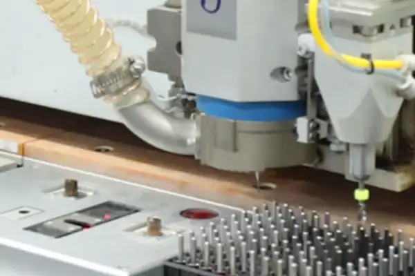
Manufacturing adds another layer of complexity. You might think the job is done once you hand the design files to the factory, but there are so many variables involved. The same design can yield vastly different performance results depending on the factory. Drilling precision, copper foil surface roughness, dielectric layer uniformity—every step affects the final product’s electrical characteristics. This is especially critical for high-frequency applications, where poor control over manufacturing tolerances can cause impedance to deviate significantly from the design specifications.
Some senior engineers I know have a habit: for critical projects, they visit the partner PCB factory in person to inspect the production processes and equipment. It’s not that they distrust the technical staff; rather, there are certain manufacturing details that you simply need to see with your own eyes to be confident about. For example, is the temperature and pressure control during multi-layer lamination precise and reliable? That’s vital for ensuring the stability of the board material’s dielectric constant. There is currently an unfortunate trend in the industry: an excessive focus on stacking new technologies while neglecting fundamental reliability validation. After all, new materials and manufacturing processes require time to mature and be perfected. Blindly jumping on the bandwagon with insufficiently validated solutions can introduce unexpected risks—especially in data center environments that demand 24/7 continuous operation, where the cost of failure is extremely high.
My perspective might be considered a bit old-school: when selecting PCBs for data centers, reliability and long-term stability should take precedence over raw performance metrics. Of course, this doesn’t mean performance isn’t important; rather, it is about striking a reasonable balance between the two. Ultimately, the massive computing networks we rely on are underpinned by tangible circuit boards, and those boards must be able to stand the test of time.
Many engineers misunderstand buried via PCBs, often viewing them as a hallmark
As an electronics engineer, I’ve learned a lot of lessons the hard
When it comes to heat dissipation, do aluminum-based boards immediately come to
- Expert en production de petites et moyennes séries
- Fabrication de circuits imprimés de haute précision et assemblage automatisé
- Partenaire fiable pour les projets électroniques OEM/ODM
Heures d'ouverture : (Lun-Sam) De 9:00 à 18:30